EP0199427A1 - Präzisionsbandlückenvergleichsspannung - Google Patents
Präzisionsbandlückenvergleichsspannung Download PDFInfo
- Publication number
- EP0199427A1 EP0199427A1 EP86300299A EP86300299A EP0199427A1 EP 0199427 A1 EP0199427 A1 EP 0199427A1 EP 86300299 A EP86300299 A EP 86300299A EP 86300299 A EP86300299 A EP 86300299A EP 0199427 A1 EP0199427 A1 EP 0199427A1
- Authority
- EP
- European Patent Office
- Prior art keywords
- transistors
- transistor
- voltage
- emitter
- base
- Prior art date
- Legal status (The legal status is an assumption and is not a legal conclusion. Google has not performed a legal analysis and makes no representation as to the accuracy of the status listed.)
- Withdrawn
Links
- 238000000034 method Methods 0.000 claims abstract description 20
- 230000008569 process Effects 0.000 claims abstract description 11
- 238000004519 manufacturing process Methods 0.000 abstract description 3
- 238000012545 processing Methods 0.000 description 9
- 238000010586 diagram Methods 0.000 description 5
- 230000003071 parasitic effect Effects 0.000 description 4
- 238000009792 diffusion process Methods 0.000 description 3
- 238000013459 approach Methods 0.000 description 2
- 230000008901 benefit Effects 0.000 description 2
- 238000013461 design Methods 0.000 description 2
- 239000007787 solid Substances 0.000 description 2
- 239000000758 substrate Substances 0.000 description 2
- 230000009471 action Effects 0.000 description 1
- 230000003321 amplification Effects 0.000 description 1
- 230000000295 complement effect Effects 0.000 description 1
- 230000000694 effects Effects 0.000 description 1
- 230000006872 improvement Effects 0.000 description 1
- 229910044991 metal oxide Inorganic materials 0.000 description 1
- 150000004706 metal oxides Chemical class 0.000 description 1
- 238000012986 modification Methods 0.000 description 1
- 230000004048 modification Effects 0.000 description 1
- 238000003199 nucleic acid amplification method Methods 0.000 description 1
- 239000004065 semiconductor Substances 0.000 description 1
- 229910052710 silicon Inorganic materials 0.000 description 1
- 239000010703 silicon Substances 0.000 description 1
Images


Classifications
-
- G—PHYSICS
- G05—CONTROLLING; REGULATING
- G05F—SYSTEMS FOR REGULATING ELECTRIC OR MAGNETIC VARIABLES
- G05F3/00—Non-retroactive systems for regulating electric variables by using an uncontrolled element, or an uncontrolled combination of elements, such element or such combination having self-regulating properties
- G05F3/02—Regulating voltage or current
- G05F3/08—Regulating voltage or current wherein the variable is DC
- G05F3/10—Regulating voltage or current wherein the variable is DC using uncontrolled devices with non-linear characteristics
- G05F3/16—Regulating voltage or current wherein the variable is DC using uncontrolled devices with non-linear characteristics being semiconductor devices
- G05F3/20—Regulating voltage or current wherein the variable is DC using uncontrolled devices with non-linear characteristics being semiconductor devices using diode- transistor combinations
- G05F3/30—Regulators using the difference between the base-emitter voltages of two bipolar transistors operating at different current densities
Definitions
- This invention relates to integrated circuit bandgap voltage references, and more particularly to bandgap voltage references capable of being implemented with CMOS (complementary metal oxide semiconductor) processing techniques.
- CMOS complementary metal oxide semiconductor
- Voltage references are required to provide a substantially constant output voltage irrespective of changes in input voltage, output current or temperature. Such references are used in many design applications, such as digital-to-analog converters, power supplies, cold junction thermistor compen- I sation circuits, analog-to-digital converters, panel meters, calibration standards, precision current sources and control set-point circuits.
- Modern voltage references are generally based on either zener diodes or bandgap generated voltages. Zener devices characteristically exhibit high-power dissipation and poor noise specifications.
- Bandgap voltage references are designed to yield stable output voltages over temperature by summing a pair of voltages with negative and positive temperature coefficients. A voltage with a negative temperature coefficient is obtained from the base-emitter junction of a transistor, while a voltage with a positive temperature coefficient is obtained from the difference between the base-emitter voltages of two transistors operating with unequal current densities.
- a voltage level with a low temperature coefficient results if the sum is equal to 1.23 volts, which is close to the bandgap voltage of silicon.
- the 1.23 volt level is then amplified to provide stable output voltages of typically 5.0 and 10.0 volts.
- a typical bipolar transistor or diode has a base-emitter voltage when the device is on of about 600mV, and a negative temperature coefficient of about -2mV/°C.
- the positive temperature coefficient voltage obtained from the difference between the base-emitter voltages of two transistors is typically about 60mV at 25°C if the current densities of the two transistors are in a 10:1 ratio, and has to be amplified before being added to the base-emitter of the first transistor in order to achieve a 1.23 voltage level.
- the 60mV differential might be increased up to about 200 mV for larger but less practical devices, but amplification would still be required.
- FIG. 1 An early bandgap voltage reference is described in an article by R. Widlar in IEEE J. Solid State Circuits, Vol. S C-6, pages 2-7, February, 1971.
- a more common circuit is one developed by Paul Brokaw and described in an article entitled "A Simple Three-Terminal IC Bandgap Reference", IEEE J. Solid State Circuits, Vol. SC-9, pages 383-93, December, 1974.
- the basic approach taken in this circuit is illustrated in FIG. 1, in which a pair of bipolar transistors Ql and Q2 have their collectors connected through resistors R1 and R2, respectively, to a positive voltage bus V+ and their bases connected in common to provide a 1.23 volt reference.
- the collectors of 01 and Q2 are also connected to respective inputs to an operational amplifier Al, the output of which is connected to the voltage reference output.
- the emitters of Ql and Q2 are connected to opposite sides of resistor R3, while the emitter of Q2 is also connected through resistor R4 to ground.
- Q1 and Q2 are forced to run at different current densities by scaling the geometry of Q1 larger than that of Q2, by making Rl larger than R2, or both (a larger transistor geometry or a smaller through-current will each lead to a smaller current density).
- a voltage differential thus appears across R3, producing a temperature proportional current which also flows through R4.
- R3 and R4 an arbitrary voltage can be created across R4 which is, temperature proportional.
- the R4 voltage is added to the base-emitter voltage of Q2, producing a relatively stable reference output.
- FIG. 1 circuit can be implemented with standard bipolar processing, it unfortunately is not readily adaptable to CMOS processing techniques which are presently becoming very widespread.
- CMOS processing the transistor collectors are formed from the substrate, which is held at V+; Rl and R2 would thus be shorted out if.FIG. 1 was implemented using CMOS processing. Extra process steps could be added to get around this problem, but this would be a costly alternative,
- the standard P-well CMOS process has available parasitic NPN bipolar transistors, but the collectors are not individually accessible and are all connected to V+.
- Such a transistor is illustrated in FIG. 2. It. is fabricated using an N+ (heavily doped) source/drain diffusion 2 as the_ emitter, the P well 4 accessed through a P+ diffusion 6 as the base, and the N- (lightly doped) substrate 8 accessed through an N+ diffusion 10 as the collector.
- the polarities of the various components would be reversed for an N-well CMOS process.
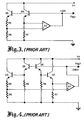
- FIG. 3 Several alternative arrangement of the FIG. 1 circuit have been proposed or used to form a CMOS voltage reference using parasitic bipolar transistors such as that illustrated in FIG. 2.
- FIG. 3 One such arrangement is shown in FIG. 3.
- the collectors of transistors Q3 and Q4 are connected directly to V+, and their bases are connected to the 1.23 volt reference output.
- the emitter of Q3 is connected to a resistive voltage divider circuit consisting of series connected resistors R5 and R6, while the emitter of Q4 is connected to a resistor R7; the opposite sides of R6 and R7 are both grounded.
- An operational amplifier A2 has its inputs connected respectively to the emitter of Q4 and to the junction of R5 and R6, and its output connected to the voltage reference output.
- Amplifier A2 directly amplifies the differential base-emitter voltage term appearing across R5, and forces the output reference voltage in a manner similar to the FIG. 1 circuit.
- Different current densities are provided for Q3 and Q4 by making Q3 larger than Q4, R6 larger than R7, or both.
- FIG. 3 circuit One problem with the FIG. 3 circuit is in the required precision for amplifier A2. Even if the current densities in Q3 and Q4 differ by a factor of 100, which is probably about the limit of practicality, only about 120mV appears across R5. Since A2 is fabricated with MOS devices, it could have an input offset as high as 20mV even with a careful design. This would produce about a 16% error in the base-emitter voltage differential term (20mV/120mV) and about an 8% error in the output reference voltage. Additionally, the temperature coefficient of the offset voltage is not predictable and can cause the output voltage to drift with temperature.
- FIG. 4 One method of improving on the circuit of FIG. 3 involves stacking NPN transistors to increase the base-emitter voltage differential term. This approach is illustrated in FIG. 4, in which the bases of transistors Q3 and Q4 are shown connected to the emitters of transistors Q5 and Q6, respectively, and the collectors of all four transistors are connected to V+. Resistors R5, R6 and R7 together with operational amplifier A2 are connected to the emitters of Q3 and Q4 as in FIG. 3, but the voltage reference output is connected to the bases of 05 and Q6, rather than to Q3 and Q4. The bases of the two latter transistors are held above ground by resistors R8 and R9, respectively.
- Another object is the provision of such a bandgap voltage reference circuit which is compatible with both bipolar and CMOS processing techniques.
- a bandgap voltage reference circuit which includes first and second sets of bipolar transistors connected to accumulate the base-emitter voltages of each set, and means for transmitting respective current flows through the collector-emitter circuits of each of the transistors.
- the number of transistors in each set, the geometry of each transistor and the currents transmitted through the various transistors are selected such that the accumulated base-emitter voltages of the first and second sets differ by an amount corresponding to a predetermined bandgap voltage.
- Output means are connected to present the accumulated base-emitter voltage differential between the two transistor sets as a high precision reference voltage.
- the first transistor set includes one more transistor than the second set.
- Individual current sources are provided for each transistor in each set, with the currents through the transistors of the first set being larger than the currents for the second set.
- the second set transistors are scaled larger than the first set transistors. Therefore, the current densities through the transistors of the first set exceed the current densities of the second set. The result is a greater base-emitter voltage for each transistor in the first set, and an accumulated base-emitter voltage differential between the two sets of 1.23 volts. If the circuit elements used are formed from a typical CMOS process, a difference in current densities of about 100:1 will normally be required.
- the bandgap reference may be taken directly from the voltage differential between the emitters of the last transistors in each set.
- the emitters of the last transistors in each set may be connected to respective inputs of an operational amplifier. This forces the accumulated base-emitter voltage differentials between the two sets to appear across the bases of the first transistors in each set.
- the bases of those transistors are then connected in circuit with another operational amplifier and a ground referenced voltage divider circuit to produce a ground referenced bandgap output.
- Another alternate embodiment when the circuit is produced by a bipolar process involves connecting the transistors of both sets as diodes and providing single current sources for each set, thus eliminating all but two of the current sources.
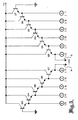
- FIG. 5 A schematic diagram of a bandgap voltage reference circuit which has a considerably lower offset voltage error than in the prior art and is compatible with both bipolar and CMOS processing techniques is shown in FIG. 5.
- Six transistors, Q7, Q8, Q9, Q10, Q11 and Q12, are connected in succession with the emitter of each transistor except for the last transistor Q12 connected to the base of the next transistor.
- the collectors of each of the transistors are connected to a positive voltage bus V+, while their emitters are connected to respective current sources I7, 18, 19, I10, I11 and 112.
- the base of the first transistor Q7 is grounded, and the emitter of Q12 is connected to an output terminal 12.
- a second set of transistors consisting of Q13, Q14, Q 15, Q16 and Q17 is connected in succession on the left hand side of the circuit, with the emitter of each transistor in the second set except for the last transistor Q17 connected to the base of the next transistor.
- the collectors of each of the transistors are connected to positive voltage bus V+, and their emitters are connected to respective current sources 1 13, 114, 115, I16 and I17.
- the base of the first transistor Q 13 in the second set is grounded, while the emitter of the last transistor Q17 is connected to an output terminal 14.
- the first set of transistors Q7-Q12 includes one more transistor than the second set Q13-Q14, and thus the voltage at output terminal 12 will reflect one more base-emitter voltage drop than will the voltage at output terminal 14.
- the geometries of transistors Q7-Q12 are scaled smaller than the corresponding geometries of transistors Q13-Q17, and 17-112 draw greater currents through the collector-emitter circuits of their respective transistors than do 113-117. The result of both the size and current scalings is to produce current densities through Q7-Q12 which are larger than the current densities through Q13-Q17.
- the number of transistors employed in each set is somewhat arbitrary. The use of a larger number of transistors will reduce the geometric scaling ratio, required, but will take up more area. Fewer transistors would reduce the required area, but would increase the geometric scaling ratio. Regardless of the absolute number of transistors in each set, however, it is preferable that the first set have one more transistor than the second set. A base-emitter voltage term is then added to a differential base-emitter voltage term to produce the desired temperature stable bandgap reference.
- FIG. 5 circuit has a lower error component than prior art CMOS circuits, one disadvantage is that the reference voltage across output terminals 12, 14 is floating and not referenced to ground.
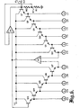
- FIG. 6 A variation of the circuit which provides an adjustable ground referenced output voltage is shown in FIG. 6.
- Q7-Q17 and 17-117 are implemented essentially as in the circuit of FIG. 5. However, instead of being taken directly as an output, the emitters of Q12 and Q17 are connected to the inputs of an operational amplifier A3.
- the effect of this connection is to substantially equalize the emitter voltages of Q12 and Q17, and force the former output of 1.23 volts to be reflected back through the two transistor sets as a voltage differential between the bases of the first transistors Q7 and Q13 of each set.
- the bases of Q7 and Q13 are connected respectively to an output terminal 16, and to the inverting input of another operational amplifier A4, with the output of A3 connected in common with the base of Q13 to the inverting input of A4.
- the base of Q7 is connected to the output of A4 and to one end of a voltage divider circuit consisting of series connected resistors R 10 and 11.
- the non-inverting input to A4 is taken from an intermediate point 18 in the voltage divider circuit at the junction of R10 and Rll.
- A4 The action of A4 is to raise the voltage at output terminal 16 until the base voltage of Q13 is equal to the voltage at junction 18, thus causing the two inputs to A4 to equalize in voltage. Accordingly, the 1.23 volts established between the bases of Q7 and Q13 also appears across R10. Under these conditions the output voltage at terminal 16 is ground referenced and equal to 1.23V times (R10+ R11)/R11.
- This circuit has the added advantage that a more precise output voltage can be obtained than in the prior art even if ampli- .fiers A3 and A4 are not as accurate as the amplifiers employed in prior circuits, since A3 and A4 amplify 1.23 volts rather than a much smaller voltage as in the prior art.
- FIG. 7 Another embodiment of the invention which is particularly adapted for a bipolar fabrication process is shown in FIG. 7.
- the first set consists of nominally six transistors Q18, Q19, Q20, Q21, Q22 and Q23, while the second set consists of nominally five transistors Q24, Q25, Q26, Q27 and Q28.
- the emitter of each transistor except for the last one in each set is connected to the base of the following transistor, as in FIG. 5.
- each of the transistors in FIG. 7 functions as a diode by having its collector shorted to its base.
- the bases of the first transistor in each set Q18 and Q24 are no longer grounded, but rather are connected along with their collectors to V+.
- the transistors of each set are connected in series, with only the first transistor of each set connected to V+.
- One current source 118 is connected to the emitter of Q23 and draws current through each of the transistors Q18-Q23, while another current source I19 is connected to the emitter of Q28 and draws current through each of the transistors Q 24-Q28.
- the geometric scalings of the transistors and the two current sources are selected as in the circuit of FIG. 5 to establish a bandgap reference voltage of 1.23 volts across output terminals 20 and 22 at the emitters of Q23 and Q28, respectively.
Landscapes
- Engineering & Computer Science (AREA)
- Microelectronics & Electronic Packaging (AREA)
- Physics & Mathematics (AREA)
- Power Engineering (AREA)
- Nonlinear Science (AREA)
- Electromagnetism (AREA)
- General Physics & Mathematics (AREA)
- Radar, Positioning & Navigation (AREA)
- Automation & Control Theory (AREA)
- Control Of Electrical Variables (AREA)
- Semiconductor Integrated Circuits (AREA)
Applications Claiming Priority (2)
| Application Number | Priority Date | Filing Date | Title |
|---|---|---|---|
| US72540485A | 1985-04-22 | 1985-04-22 | |
| US725404 | 1985-04-22 |
Publications (1)
| Publication Number | Publication Date |
|---|---|
| EP0199427A1 true EP0199427A1 (de) | 1986-10-29 |
Family
ID=24914422
Family Applications (1)
| Application Number | Title | Priority Date | Filing Date |
|---|---|---|---|
| EP86300299A Withdrawn EP0199427A1 (de) | 1985-04-22 | 1986-01-17 | Präzisionsbandlückenvergleichsspannung |
Country Status (2)
| Country | Link |
|---|---|
| EP (1) | EP0199427A1 (de) |
| JP (1) | JPS61244058A (de) |
Cited By (5)
| Publication number | Priority date | Publication date | Assignee | Title |
|---|---|---|---|---|
| FR2642916A1 (fr) * | 1989-02-08 | 1990-08-10 | Burr Brown Corp | Procede et circuit pour produire une tension de reference stable et a faible bruit |
| EP0550680A4 (en) * | 1990-09-28 | 1993-09-22 | Analog Devices, Incorporated | Cmos voltage reference with stacked base-to-emitter voltages |
| EP0602466A3 (de) * | 1992-12-18 | 1995-03-29 | Itt Ind Gmbh Deutsche | Monolithisch integrierter Spannungsregler. |
| CN103677037A (zh) * | 2012-09-11 | 2014-03-26 | 意法半导体研发(上海)有限公司 | 用于生成带隙基准电压的电路和方法 |
| CN112859993A (zh) * | 2021-01-08 | 2021-05-28 | 中国科学院微电子研究所 | 高压带隙基准电压源及其产生方法、高压固定电源及其应用 |
Citations (2)
| Publication number | Priority date | Publication date | Assignee | Title |
|---|---|---|---|---|
| US4224537A (en) * | 1978-11-16 | 1980-09-23 | Motorola, Inc. | Modified semiconductor temperature sensor |
| JPS5936826A (ja) * | 1982-08-25 | 1984-02-29 | Nec Corp | 定電圧発生回路 |
-
1985
- 1985-09-06 JP JP19752985A patent/JPS61244058A/ja active Pending
-
1986
- 1986-01-17 EP EP86300299A patent/EP0199427A1/de not_active Withdrawn
Patent Citations (2)
| Publication number | Priority date | Publication date | Assignee | Title |
|---|---|---|---|---|
| US4224537A (en) * | 1978-11-16 | 1980-09-23 | Motorola, Inc. | Modified semiconductor temperature sensor |
| JPS5936826A (ja) * | 1982-08-25 | 1984-02-29 | Nec Corp | 定電圧発生回路 |
Non-Patent Citations (4)
| Title |
|---|
| IEEE JOURNAL OF SOLID-SATE CIRCUITS, vol.SC-17, no. 6, December 1982, pages 1139-1143, IEEE, New York, US; G.C.M. MEIJER et al.: "A new curvature-corrected bandgap reference" * |
| IEEE JOURNAL OF SOLID-STATE CIRCUITS, vol.SC-19, no. 6, December 1984, pages 892-899, IEEE, New York, US; B.K. AHUJA et al.: "A programmable CMOS dual channel interface processor for telecommunications applications" * |
| IEEE JOURNAL OF SOLID-STATE CIRCUITS, vol.SC-8, no. 3, June 1973, pages 222-226, IEEE, New York, US; K.E. KUIJK: "A precision reference voltage source" * |
| PATENTS ABSTRACTS OF JAPAN, vol. 8, no. 137 (P-282) [1574], 26th June 1984; & JP - A - 59 36 826 (NIPPON DENKI K.K.) 29-02-1984 * |
Cited By (6)
| Publication number | Priority date | Publication date | Assignee | Title |
|---|---|---|---|---|
| FR2642916A1 (fr) * | 1989-02-08 | 1990-08-10 | Burr Brown Corp | Procede et circuit pour produire une tension de reference stable et a faible bruit |
| EP0550680A4 (en) * | 1990-09-28 | 1993-09-22 | Analog Devices, Incorporated | Cmos voltage reference with stacked base-to-emitter voltages |
| EP0602466A3 (de) * | 1992-12-18 | 1995-03-29 | Itt Ind Gmbh Deutsche | Monolithisch integrierter Spannungsregler. |
| US5446380A (en) * | 1992-12-18 | 1995-08-29 | Deutsche Itt Industries Gmbh | Monolithic integrated voltage regulator |
| CN103677037A (zh) * | 2012-09-11 | 2014-03-26 | 意法半导体研发(上海)有限公司 | 用于生成带隙基准电压的电路和方法 |
| CN112859993A (zh) * | 2021-01-08 | 2021-05-28 | 中国科学院微电子研究所 | 高压带隙基准电压源及其产生方法、高压固定电源及其应用 |
Also Published As
| Publication number | Publication date |
|---|---|
| JPS61244058A (ja) | 1986-10-30 |
Similar Documents
| Publication | Publication Date | Title |
|---|---|---|
| US4123698A (en) | Integrated circuit two terminal temperature transducer | |
| EP0429198B1 (de) | Bandgapreferenzspannungsschaltung | |
| US3800239A (en) | Current-canceling circuit | |
| EP0072589B1 (de) | Stromstabilisierungsanordnung | |
| JPS61187020A (ja) | 電圧基準回路 | |
| JPH01143510A (ja) | 二端子温度補償式電流源回路 | |
| US4243898A (en) | Semiconductor temperature sensor | |
| US4475077A (en) | Current control circuit | |
| US4224537A (en) | Modified semiconductor temperature sensor | |
| US6765431B1 (en) | Low noise bandgap references | |
| US6483372B1 (en) | Low temperature coefficient voltage output circuit and method | |
| US5699010A (en) | Differential amplifier circuit | |
| US6288525B1 (en) | Merged NPN and PNP transistor stack for low noise and low supply voltage bandgap | |
| US4931718A (en) | CMOS voltage reference | |
| EP0350857B1 (de) | Völlig differentielle Referenzspannungsquelle | |
| JPS6326895B2 (de) | ||
| EP0199427A1 (de) | Präzisionsbandlückenvergleichsspannung | |
| EP0443239A1 (de) | Stromspiegel mit Basisstromkompensation | |
| US4779061A (en) | Current-mirror arrangement | |
| US4577119A (en) | Trimless bandgap reference voltage generator | |
| US4378529A (en) | Differential amplifier input stage capable of operating in excess of power supply voltage | |
| JP3138203B2 (ja) | 基準電圧発生回路 | |
| JPH0844449A (ja) | 定電圧回路 | |
| US5721512A (en) | Current mirror with input voltage set by saturated collector-emitter voltage | |
| US3990017A (en) | Current amplifier |
Legal Events
| Date | Code | Title | Description |
|---|---|---|---|
| PUAI | Public reference made under article 153(3) epc to a published international application that has entered the european phase |
Free format text: ORIGINAL CODE: 0009012 |
|
| AK | Designated contracting states |
Kind code of ref document: A1 Designated state(s): DE FR GB |
|
| STAA | Information on the status of an ep patent application or granted ep patent |
Free format text: STATUS: THE APPLICATION IS DEEMED TO BE WITHDRAWN |
|
| 18D | Application deemed to be withdrawn |
Effective date: 19870504 |
|
| RIN1 | Information on inventor provided before grant (corrected) |
Inventor name: BOWERS, DEREK F. |