EP0199602A2 - Circuit de traitement du signal - Google Patents
Circuit de traitement du signal Download PDFInfo
- Publication number
- EP0199602A2 EP0199602A2 EP86303153A EP86303153A EP0199602A2 EP 0199602 A2 EP0199602 A2 EP 0199602A2 EP 86303153 A EP86303153 A EP 86303153A EP 86303153 A EP86303153 A EP 86303153A EP 0199602 A2 EP0199602 A2 EP 0199602A2
- Authority
- EP
- European Patent Office
- Prior art keywords
- circuit
- output
- signal
- comparing
- converter
- Prior art date
- Legal status (The legal status is an assumption and is not a legal conclusion. Google has not performed a legal analysis and makes no representation as to the accuracy of the status listed.)
- Granted
Links
Images


Classifications
-
- H—ELECTRICITY
- H04—ELECTRIC COMMUNICATION TECHNIQUE
- H04N—PICTORIAL COMMUNICATION, e.g. TELEVISION
- H04N9/00—Details of colour television systems
- H04N9/64—Circuits for processing colour signals
Definitions
- the present invention relates to a video signal processing circuit for use in a video tape recorder (VTR), television set,and the like.
- VTR video tape recorder
- the spectra of the chrominance signal (hereinafter to be briefly called C signal) are interleaved between those of the luminance signal at intervals of the horizontal scanning period (the period to be briefly called 1 H).
- the luminance signal (to be briefly called Y signal) is separated from the input video signal by a Y type comb filter which adds a 1 H delayed video signal to the input video signal, and the chrominance signal is separated from the input video signal by a C type comb filter which subtracts the 1 H delayed video signal from the input video signal.
- the comb filters are used in the so-called Y/C separating circuit.
- the C type comb filter is used also in the color S/N improving circuit for the VTR.
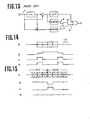
- FIG. 13 A simplified block diagram of this prior art method is shown in Fig. 13. According to this construction, when a chrominance signal as shown by a in Fig. 14 is inputted, a signal b as a detected output by the C type comb filter and a signal c as a detected output by the Y type comb filter are passed through an AND gate 81, and a signal as indicated by d is thereby outputted.
- An object of the present invention is to provide a signal processing circuit which is capable of accurately detecting the vertical correlation of the chrominance signal.
- the signal, processing circuit of the invention detects the absence of vertical correlation of the chrominance signal by comparing a vertical correlation of amplitude level and that of phase of the chrominance signal.
- the signal processing circuit of the present invention comprises a converter for converting a change in the vertical direction of each of amplitude and phase of an input chrominance signal into a change in the direction of amplitude, and a comparing circuit for comparing the amplitude level of a delayed signal by a predetermined time period of the output of the converter with the amplitude level of the output of the converter, whereby the vertical correlation of the input chrominance signal is detected.
- the present invention with the above described structure makes it possible that a change in the vertical direction of each of amplitude level and phase of a chrominance signal is detected, and thereby, presence and absence of vertical correlation of the chrominance signal is certainly detected.
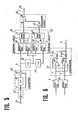
- Fig. 1 is a block diagram of a first preferred embodiment of the invention.
- a chrominance signal input to an input terminal 1 is passed through a band pass filter (BPF) 14 and sent to a converter 9 consisting of a 1 H delay circuit 2 and a subtractor 3, where a change of phase in the vertical direction of the chrominance signal is converted into a change of amplitude.
- BPF band pass filter
- the chrominance signal is then sent to a comparing circuit 10, that is, the same is, on one hand, sent to a detector 5 via a 1 H delay circuit 4, and, on the other hand, sent to a detector 6.
- Outputs of the detectors 5 and 6 are compared by a comparator 7 and when the level difference is large enough, a signal of High level, for example, is output from an output terminal 8.
- FIG. 2 An example of the comparator 7 is shown in Fig. 2.
- the output of the detector 5 is connected to a negative input of a comparator 11 and a positive input of a comparator 12, and the output of the detector 6 is connected to a positive input of the comparator 11 and a negative input of the comparator 12.
- Outputs of the comparators 11, 12 are subjected to an OR operation for the high level by diodes 13 and 14 and sent to the output terminal 8. Operations of various parts of the present invention as constructed above will be described below referring to the waveform diagrams of Figs. 3 and 4.
- the input signal a is converted into a chrominance signal b by means of a comb filter, then detected and made into signals c and d by the detectors 5, 6, and the same are then turned into signals e, f in the comparator 7 and output as a signal g through an OR operation thereby.
- the signal g includes the period z during which there is no vertical correlation of the chrominance signal.
- the input signal a is converted into a chrominance signal b by means of the comb filter, then detected and made into signals c and d by the detectors 5, 6, and the same are then turned into signals e, f in the comparator 7 and output as a signal g.
- the signal g includes the period z during which there is no vertical correlation of hue, which has never been detected by a prior art device. That is, two sets of 1 H delay circuits 2 have been used in this case as shown in Fig.
- the band pass filter 14 in the present case may be disposed in the succeeding stage to the subtractor 3, may be disposed in the preceding stage to the detectors 5, 6, or may be eliminated.
- Fig. 5 is a block diagram of the second preferred embodiments of the invention.
- a chrominance signal input to an input terminal 21 is passed through a band pass filter 22 and sent to a converter 23 consisting of a 1 H delay circuit 24 and a combining circuit, or, a subtractor 25, where a change of phase in the vertical direction of the chrominance signal is converted into a change of amplitude.
- the chrominance signal is sent to a delay circuit 26 and to a comparing circuit 28, the output of the delay circuit 26 is sent to a delay circuit 27 and to the comparing circuits 28 and 32, and the output of the delay circuit 27 is sent to the comparing circuit 32.
- the input signals are detected by detectors 29, 30 and the detected signals are compared by a comparator 31, and if the level difference is large enough, a signal of High level is output to an operational circuit 36. Similar operations are made in the comparing circuit 32, also.
- the operational circuit 36 is constituted of an inverter circuit 37 and an AND circuit 38, for example, and operates such that, if the output of the comparing circuit 28 is "1" and the output of the comparing circuit 32 is "0", the same delivers an output of "1". As a matter of course, this polarity may be opposite if the circuits in the succeeding stages are arranged accordingly.
- the input signal a is converted into a chrominance signal b by means of a comb filter, then detected and made into signals c and d by the detectors 29, 30, and the same are then turned into signals f, g in the comparator 31 and output as a signal h through an OR operation thereby.
- signals d, e are provided through detection by detectors 33, 34 and the same are output from the comparator 35 as a signal i.
- a signal j is output.
- the signal j indicates the period z during which there is no vertical correlation of the chrominance signal.
- the input signal a is converted into a chrominance signal b by means of the comb filter 23 as a converter, then detected and made into signals c and d by the detectors 29, 30, and the same are then turned into signals f, g in the comparator 31 and output as a signal h.
- a signal i is output.
- a signal j is output.
- the signal j indicates the period z during which there is no vertical correlation of hue, which has never been detected by a prior art device.
- the change of hue in the vertical direction has been converted into the change of color in the direction of amplitude by the converter constituted of the 1 H delay circuit as shown in Fig. 5, whereby the detection of the change of hue in the vertical direction which was unachievable by a prior art device has been made possible.
- the band pass filter 22 in the present case may be disposed in the succeeding stage to the subtractor 25, may be disposed in the preceding stage to the detectors 29, 30, 33, 34, or may be eliminated.
- the output signals of the detector 30 and the detector 33 are the same signal, it is possible to eliminate, for example, the detector 33 and adapt the output of the detector 30 to be input to the comparator 35.
- Fig. 9 is a block diagram of the third preferred embodiment of the invention.
- a signal input to an input terminal 51 is passed through a band pass filter 52 and sent to a converter 53 consisting of a 1 H delay circuit 54 and a subtractor 55, where a change of phase in the vertical direction of the chrominance signal is converted into a change of amplitude.
- the chrominance signal is sent to a delay circuit 56 and to a comparing circuit 57, and the output of the delay circuit 56 is sent to a comparing circuit 57.
- the input signal is detected by detectors 58, 59 and the detected outputs are compared by a comparator 60, and if the level difference is large enough, a signal of High level is output to an operational circuit 62 and also to a delay circuit 61.
- the output from the delay circuit 61 is sent to the operational circuit 62.
- the operational circuit 62 is constituted of an inverter circuit 63 and an AND circuit 64, for example, and operates such that, if the output of the comparing circuit 57 is "1" and the output of the delay circuit 61 is "0", only then, the same delivers an output of "1".
- this polarity may be opposite if the circuits in the succeeding stages are arranged accordingly.
- comparator 60 While an example of the comparator 60 is shown in Fig. 10, it is the same as the example that was shown in Fig. 2.
- amplitude of the chrominance signal includes a change in the vertical direction is indicated in Fig. 11, in which the diagrams a - j indicate the waveforms corresponding to the portions a - j in Figs. 9 and 10.
- the input signal a is converted into a chrominance signal b by means of a comb filter 53 as a converter, then detected and made into signals c and d by the detectors 58, 59, and the same are then turned into signals e, f in the comparator 60 and output as a signal g through an OR operation thereby to an operational circuit 62.
- the signal g is also sent to a delay circuit 61 to be delayed by 1 H and sent to the operational circuit 62.
- a signal i is output.
- the signal i indicates the period z during which there is no vertical correlation of the chrominance signal.
- the input signal a is converted into a chrominance signal b by means of the comb filter 53 as a converter, then detected and made into signals c and d by the detectors 58, 59, and the same are then turned into signals e, f in the comparator 60 and output therefrom as a signal g to the operational circuit 62.
- the signal g is delayed by 1 H in the delay circuit 61 and delivered to the operational circuit 62 as a signal h.
- a signal i is output.
- the signal i indicates the period z during which there is no vertical correlation of hue, which has never been detected by a prior art device.
- the change of hue in the vertical direction has been converted into the change of color in the direction of amplitude by the converter constituted of the 1 H delay circuit as shown in Fig. 9, whereby the detection of the change of hue in the vertical direction which was unachievable by a prior art device has been made possible.
- the band pass filter 52 in the present case may be disposed in the succeeding stage to the subtractor 55, may be disposed in the preceding stage to the detectors 58, 59, or may be eliminated.
Landscapes
- Engineering & Computer Science (AREA)
- Multimedia (AREA)
- Signal Processing (AREA)
- Processing Of Color Television Signals (AREA)
Applications Claiming Priority (6)
| Application Number | Priority Date | Filing Date | Title |
|---|---|---|---|
| JP60089218A JPS61247186A (ja) | 1985-04-25 | 1985-04-25 | 信号処理回路 |
| JP89218/85 | 1985-04-25 | ||
| JP277103/85 | 1985-12-10 | ||
| JP27710385A JPH0671337B2 (ja) | 1985-12-10 | 1985-12-10 | 信号処理回路 |
| JP277104/85 | 1985-12-10 | ||
| JP27710485A JPH0671338B2 (ja) | 1985-12-10 | 1985-12-10 | 信号処理回路 |
Publications (3)
| Publication Number | Publication Date |
|---|---|
| EP0199602A2 true EP0199602A2 (fr) | 1986-10-29 |
| EP0199602A3 EP0199602A3 (en) | 1988-07-20 |
| EP0199602B1 EP0199602B1 (fr) | 1992-03-18 |
Family
ID=27306066
Family Applications (1)
| Application Number | Title | Priority Date | Filing Date |
|---|---|---|---|
| EP86303153A Expired EP0199602B1 (fr) | 1985-04-25 | 1986-04-25 | Circuit de traitement du signal |
Country Status (3)
| Country | Link |
|---|---|
| US (1) | US4734758A (fr) |
| EP (1) | EP0199602B1 (fr) |
| DE (1) | DE3684353D1 (fr) |
Families Citing this family (6)
| Publication number | Priority date | Publication date | Assignee | Title |
|---|---|---|---|---|
| JP2570717B2 (ja) * | 1987-02-03 | 1997-01-16 | ソニー株式会社 | くし形フイルタ |
| US4809060A (en) * | 1987-09-10 | 1989-02-28 | Rca Licensing Corporation | Hanging dot reduction arrangement |
| US5025311A (en) * | 1987-12-28 | 1991-06-18 | Matsushita Electric Industrial Co., Ltd. | Video signal separating apparatus |
| JPH01264089A (ja) * | 1988-04-14 | 1989-10-20 | Olympus Optical Co Ltd | 高輝度着色防止回路 |
| DE3836043A1 (de) * | 1988-10-20 | 1990-04-26 | Thomson Brandt Gmbh | Schaltung fuer ein adaptives kammfilter zur trennung von leuchtdichtesignal und farbartsignal eines fbas-pal-signals |
| US6469741B2 (en) | 1993-07-26 | 2002-10-22 | Pixel Instruments Corp. | Apparatus and method for processing television signals |
Family Cites Families (7)
| Publication number | Priority date | Publication date | Assignee | Title |
|---|---|---|---|---|
| JPS50102218A (fr) * | 1974-01-09 | 1975-08-13 | ||
| US4178609A (en) * | 1977-10-25 | 1979-12-11 | The Magnavox Company | Comb filter having improved luminance response |
| GB2055495B (en) * | 1979-08-01 | 1983-07-06 | British Broadcasting Corp | Movement detector for television signals |
| US4263612A (en) * | 1979-08-01 | 1981-04-21 | Rca Corporation | Comb filter equalization circuit |
| US4240105A (en) * | 1979-08-20 | 1980-12-16 | Yves C. Faroudja | Method and apparatus for separation of chrominance and luminance with adaptive comb filtering in a quadrature modulated color television system |
| NL8004312A (nl) * | 1980-07-28 | 1982-03-01 | Philips Nv | Bewegingsdetectieschakeling. |
| JPS59117887A (ja) * | 1982-12-24 | 1984-07-07 | Victor Co Of Japan Ltd | 映像信号補正回路 |
-
1986
- 1986-04-22 US US06/854,746 patent/US4734758A/en not_active Expired - Lifetime
- 1986-04-25 DE DE8686303153T patent/DE3684353D1/de not_active Expired - Lifetime
- 1986-04-25 EP EP86303153A patent/EP0199602B1/fr not_active Expired
Also Published As
| Publication number | Publication date |
|---|---|
| DE3684353D1 (de) | 1992-04-23 |
| US4734758A (en) | 1988-03-29 |
| EP0199602A3 (en) | 1988-07-20 |
| EP0199602B1 (fr) | 1992-03-18 |
Similar Documents
| Publication | Publication Date | Title |
|---|---|---|
| US4825289A (en) | Noise reduction apparatus for video signal | |
| EP0173439B1 (fr) | Circuit de séparation des signaux de luminance et de chrominance | |
| KR940009481B1 (ko) | Y/c 분리장치 | |
| KR900009063B1 (ko) | 반송 색 신호 처리 회로 | |
| US4734758A (en) | Signal processing circuit | |
| KR930003177B1 (ko) | 휘도신호와 색신호 분리용 패턴 적응형 디지탈 콤 필터 | |
| US5400082A (en) | Device for reducing noise in a composite video signal | |
| US4694331A (en) | Vertical transition processor for a comb filter | |
| JP2750572B2 (ja) | 画像変化の検出器 | |
| JP2506530B2 (ja) | 画像信号の輝度信号及び色信号分離装置 | |
| US4862252A (en) | Y/C separator circuit for separating luminance and chrominance signals conditioned on an ac luminance component | |
| US5491522A (en) | Luminance and color signal isolation device | |
| US5500687A (en) | Chrominance signal separator using chrominance signal correlation | |
| KR900005604B1 (ko) | 상관검출장치와 그것을 사용한 영상신호 기록재생장치 | |
| KR910008395B1 (ko) | 재생 반송색신호 처리회로 | |
| EP0668702B1 (fr) | Circuit de séparation des signaux de luminance et de chrominance | |
| JPH0671337B2 (ja) | 信号処理回路 | |
| KR0119489Y1 (ko) | 칼라 킬러 검출 장치 | |
| JPH0671338B2 (ja) | 信号処理回路 | |
| JP2740209B2 (ja) | Y/c分離回路 | |
| JPH1175085A (ja) | ディジタル同期分離装置 | |
| JPS61247186A (ja) | 信号処理回路 | |
| JPH0644220Y2 (ja) | 輝度/色度分離回路 | |
| JPS61144997A (ja) | くし形フイルタ | |
| JP3950564B2 (ja) | ノイズレベル検出回路 |
Legal Events
| Date | Code | Title | Description |
|---|---|---|---|
| PUAI | Public reference made under article 153(3) epc to a published international application that has entered the european phase |
Free format text: ORIGINAL CODE: 0009012 |
|
| AK | Designated contracting states |
Kind code of ref document: A2 Designated state(s): DE FR GB |
|
| PUAL | Search report despatched |
Free format text: ORIGINAL CODE: 0009013 |
|
| AK | Designated contracting states |
Kind code of ref document: A3 Designated state(s): DE FR GB |
|
| 17P | Request for examination filed |
Effective date: 19890113 |
|
| 17Q | First examination report despatched |
Effective date: 19910213 |
|
| GRAA | (expected) grant |
Free format text: ORIGINAL CODE: 0009210 |
|
| AK | Designated contracting states |
Kind code of ref document: B1 Designated state(s): DE FR GB |
|
| REF | Corresponds to: |
Ref document number: 3684353 Country of ref document: DE Date of ref document: 19920423 |
|
| ET | Fr: translation filed | ||
| PLBE | No opposition filed within time limit |
Free format text: ORIGINAL CODE: 0009261 |
|
| STAA | Information on the status of an ep patent application or granted ep patent |
Free format text: STATUS: NO OPPOSITION FILED WITHIN TIME LIMIT |
|
| 26N | No opposition filed | ||
| PGFP | Annual fee paid to national office [announced via postgrant information from national office to epo] |
Ref country code: FR Payment date: 19960410 Year of fee payment: 11 |
|
| PGFP | Annual fee paid to national office [announced via postgrant information from national office to epo] |
Ref country code: GB Payment date: 19960416 Year of fee payment: 11 |
|
| PG25 | Lapsed in a contracting state [announced via postgrant information from national office to epo] |
Ref country code: GB Effective date: 19970425 |
|
| GBPC | Gb: european patent ceased through non-payment of renewal fee |
Effective date: 19970425 |
|
| PG25 | Lapsed in a contracting state [announced via postgrant information from national office to epo] |
Ref country code: FR Free format text: LAPSE BECAUSE OF NON-PAYMENT OF DUE FEES Effective date: 19971231 |
|
| REG | Reference to a national code |
Ref country code: FR Ref legal event code: ST |
|
| PGFP | Annual fee paid to national office [announced via postgrant information from national office to epo] |
Ref country code: DE Payment date: 20000427 Year of fee payment: 15 |
|
| PG25 | Lapsed in a contracting state [announced via postgrant information from national office to epo] |
Ref country code: DE Free format text: LAPSE BECAUSE OF NON-PAYMENT OF DUE FEES Effective date: 20020201 |