EP0200082B1 - Hochtemperatur Abhebeverfahren ohne Zwischenschicht für eine strukturierte Zwischenverbindungsschicht - Google Patents
Hochtemperatur Abhebeverfahren ohne Zwischenschicht für eine strukturierte Zwischenverbindungsschicht Download PDFInfo
- Publication number
- EP0200082B1 EP0200082B1 EP86105142A EP86105142A EP0200082B1 EP 0200082 B1 EP0200082 B1 EP 0200082B1 EP 86105142 A EP86105142 A EP 86105142A EP 86105142 A EP86105142 A EP 86105142A EP 0200082 B1 EP0200082 B1 EP 0200082B1
- Authority
- EP
- European Patent Office
- Prior art keywords
- layer
- polyimide layer
- temperature
- polyimide
- forming
- Prior art date
- Legal status (The legal status is an assumption and is not a legal conclusion. Google has not performed a legal analysis and makes no representation as to the accuracy of the status listed.)
- Expired
Links
Images

Classifications
-
- H—ELECTRICITY
- H10—SEMICONDUCTOR DEVICES; ELECTRIC SOLID-STATE DEVICES NOT OTHERWISE PROVIDED FOR
- H10W—GENERIC PACKAGES, INTERCONNECTIONS, CONNECTORS OR OTHER CONSTRUCTIONAL DETAILS OF DEVICES COVERED BY CLASS H10
- H10W20/00—Interconnections in chips, wafers or substrates
- H10W20/01—Manufacture or treatment
- H10W20/031—Manufacture or treatment of conductive parts of the interconnections
- H10W20/056—Manufacture or treatment of conductive parts of the interconnections by filling conductive material into holes, grooves or trenches
- H10W20/058—Manufacture or treatment of conductive parts of the interconnections by filling conductive material into holes, grooves or trenches by depositing on sacrificial masks, e.g. using lift-off
-
- H—ELECTRICITY
- H10—SEMICONDUCTOR DEVICES; ELECTRIC SOLID-STATE DEVICES NOT OTHERWISE PROVIDED FOR
- H10P—GENERIC PROCESSES OR APPARATUS FOR THE MANUFACTURE OR TREATMENT OF DEVICES COVERED BY CLASS H10
- H10P50/00—Etching of wafers, substrates or parts of devices
- H10P50/20—Dry etching; Plasma etching; Reactive-ion etching
- H10P50/28—Dry etching; Plasma etching; Reactive-ion etching of insulating materials
- H10P50/286—Dry etching; Plasma etching; Reactive-ion etching of insulating materials of organic materials
- H10P50/287—Dry etching; Plasma etching; Reactive-ion etching of insulating materials of organic materials by chemical means
-
- H—ELECTRICITY
- H10—SEMICONDUCTOR DEVICES; ELECTRIC SOLID-STATE DEVICES NOT OTHERWISE PROVIDED FOR
- H10P—GENERIC PROCESSES OR APPARATUS FOR THE MANUFACTURE OR TREATMENT OF DEVICES COVERED BY CLASS H10
- H10P76/00—Manufacture or treatment of masks on semiconductor bodies, e.g. by lithography or photolithography
- H10P76/20—Manufacture or treatment of masks on semiconductor bodies, e.g. by lithography or photolithography of masks comprising organic materials
-
- H—ELECTRICITY
- H10—SEMICONDUCTOR DEVICES; ELECTRIC SOLID-STATE DEVICES NOT OTHERWISE PROVIDED FOR
- H10P—GENERIC PROCESSES OR APPARATUS FOR THE MANUFACTURE OR TREATMENT OF DEVICES COVERED BY CLASS H10
- H10P76/00—Manufacture or treatment of masks on semiconductor bodies, e.g. by lithography or photolithography
- H10P76/20—Manufacture or treatment of masks on semiconductor bodies, e.g. by lithography or photolithography of masks comprising organic materials
- H10P76/202—Manufacture or treatment of masks on semiconductor bodies, e.g. by lithography or photolithography of masks comprising organic materials for lift-off processes
-
- H—ELECTRICITY
- H05—ELECTRIC TECHNIQUES NOT OTHERWISE PROVIDED FOR
- H05K—PRINTED CIRCUITS; CASINGS OR CONSTRUCTIONAL DETAILS OF ELECTRIC APPARATUS; MANUFACTURE OF ASSEMBLAGES OF ELECTRICAL COMPONENTS
- H05K3/00—Apparatus or processes for manufacturing printed circuits
- H05K3/10—Apparatus or processes for manufacturing printed circuits in which conductive material is applied to the insulating support in such a manner as to form the desired conductive pattern
- H05K3/14—Apparatus or processes for manufacturing printed circuits in which conductive material is applied to the insulating support in such a manner as to form the desired conductive pattern using spraying techniques to apply the conductive material, e.g. vapour evaporation
- H05K3/143—Masks therefor
-
- Y—GENERAL TAGGING OF NEW TECHNOLOGICAL DEVELOPMENTS; GENERAL TAGGING OF CROSS-SECTIONAL TECHNOLOGIES SPANNING OVER SEVERAL SECTIONS OF THE IPC; TECHNICAL SUBJECTS COVERED BY FORMER USPC CROSS-REFERENCE ART COLLECTIONS [XRACs] AND DIGESTS
- Y10—TECHNICAL SUBJECTS COVERED BY FORMER USPC
- Y10S—TECHNICAL SUBJECTS COVERED BY FORMER USPC CROSS-REFERENCE ART COLLECTIONS [XRACs] AND DIGESTS
- Y10S438/00—Semiconductor device manufacturing: process
- Y10S438/942—Masking
- Y10S438/948—Radiation resist
- Y10S438/951—Lift-off
Definitions
- the invention relates to a method of forming metal layers under high-temperature conditions.
- a patterned conductor layer on a substrate.
- the two most common methods of forming such a layer are subtractive etching and lift-off techniques.
- subtractive etching after a blanket conductor layer is deposited on the substrate, the layer is etched through a photomask in order to remove undesired portions thereof.
- lift-off a layer (typically an insulator such as polyimide) is deposited on a substrate, and is patterned through a photomask.
- the conductive layer is then desposited on the patterned insulator, and the insulator is removed from (i.e. "lifted off" of) the substrate, taking with it the undesired portions of the conductive layer.
- lift-off is more desireable in that the solvents used to remove the insulator in lift-off cause less damage to the underlaying substrate than do the etch processes (e.g. a plasma etch or a reactive ion etch) used in subtractive etching. Also, the conductor profile resulting from lift-off processing minimizes step coverage problems in subsequent conductor layers.
- etch processes e.g. a plasma etch or a reactive ion etch
- a layer of pre-imidized polyimide i.e. a copolymer of an aromatic cycloaliphatic diamine and a dianhydride
- a silicon dioxide barrier layer is formed on the polyimide.
- the barrier layer protects the polyimide layer during photolithographic processing.
- a metal layer is deposited on the structure. The polyimide layer is then stripped off the silicon, lifting off the undesired portions of the metal layer.
- the metal can be deposited at a temperature of 250 ° C-300 ° C, reducing physical faults in the deposited metal. Note that during both the deposition and lift-off of this polyimide copolymer, a harmful organic solvent such as methylene chloride must be used.
- the EP-A-0 188 735 (falling within the terms of Art. 54(3) EPC) discloses a method of forming via holes in a first polyimide layer through apertures in a second polyimide layer.
- the thickness of the second polyimide layer is varied in order to alter the slope of the via hole sidewalls.
- a first layer of polyimide is patterned through a photoresist mask. After the metal is deposited, the photoresist mask is removed from the first polyimide layer and a second polyimide layer is applied for passivation.
- barrier layers are needed in order to carry out high temperature lift-off processes.
- these special polyimides require overlaying barrier layers, which protect the polyimides from etching during the definition of a photoresist mask disposed on the barrier layer. It would be advantageous to eliminate these barrier layers, since they add to manufacturing cost.
- a process for forming a patterned interconnection layer on a processed semiconductor substrate which comprises the steps of forming a first polyimide layer on said substrate, forming a second, high-temperature polyimide layer which does not fully imidize at temperatures below 250 ° C-280 ° C on said first polyimide layer, forming a photoresist layer on said high-temperature polyimide layer, exposing said photoresist layer and developing said photoresist layer in a solvent which does not appreciably attack said high-temperature polyimide layer, etching said high-temperature polyimide layer and said first polyimide layer through said developed photoresist layer to form via holes in said first polyimide layer, said high-temperature polyimide layer and said first polyimide layer etching at substantially the same rate, said photoresist layer being substantially removed during said etching step, forming a conductor layer in said via holes on said substrate and on said etched high-temperature polyimide layer, said
- a substrate 10 has a layer of polyimide 14 spin-applied thereon. While substrate 10 is shown as being a bare silicon substrate, it is to be understood that any one of the semiconductor structures or devices currently manufactured in the industry (e.g. FET or bipolar transistors, storage capacitors, resistors, etc.) could be arranged on substrate 10, and that the patterned conductor layer to be described is patterned so as to form an electrical contact to any one of these structures. In other words, substrate 10 is shown as being bare merely for the purposes of more clearly illustrating the invention.
- semiconductor structures or devices currently manufactured in the industry e.g. FET or bipolar transistors, storage capacitors, resistors, etc.
- Polyimide layer 14 can be made up of any one of the known polyamic acid limides that are stable up to 350 ° c.
- polyimides sold under the trade names "DuPont 5878" and "DuPont 2555" by the DuPont Company of Wilmington, Delaware could be used.
- Polyimide layer 14 should be approximately as thick as the metal layer to be applied.
- polyimide layer 14 should be approximately 1.8-2.0 ⁇ m thick.
- polyimide layer 14 produces a "step" for the metal layer to cover. This enhances discontinuities in the metal layer, facilitating lift-off as described below.
- this embodiment of the invention relates to the formation of any level of metallurgy on the processed substrate.
- an additional passivating layer e.g. silicon nitride, silicon dioxide or sputtered quartz
- This additional passivating layer would have to be etched separately (i.e. etched using a separate mask) from the etching of the polyimide layers asd discussed below.
- the total thickness of the combination of polyimide 14 and the additional passivating layer should approximately equal the thickness of the metal layer to be applied.
- the combined thickness should be 1.0-1.2 /1 .m.
- the combined thickness should be 1.8-2.0 ⁇ m.
- the additional passivation layer can be made up of any insulator formed at a temperature which is less than the annealling temperature of the underlaying conductor layers. It is emphasized that while incorporation of these additional passivation layers is preferred in that they improve reliability, they can be deleted from the process of the invention if desired.
- a layer of "high-temperature” polyimide 16 is then spin-coated onto the surface of polyimide layer 14.
- Polyimide 16 can be made of any one of the known "high temperature” polyimides which do not fully imidize at temperatures below 250*C-280 °C. Such polyimides are thus compatible with high-temperature metal deposition.
- An example of such a polyimide is Pyralin PI-2566, sold by the DuPont Company of Wilmington, Delaware. "Pyralin” is a trademark of the DuPont Company.
- Another such polyimide is sold under the trade name "PIQ” by the Hitachi Chemical Co., Ltd of Japan.
- high-temperature polyimides can be distinguished from the polyimide copolymer disclosed in US-A-4,451,971 in that these polyimides are not pre-imidized, and that they can be processed using solvents commonly used in the industry. Whichever of these two high-temperature polyimides is used, polyimide layer 16 should be at least as thick as the metal layer to be deposited.
- the polyimide 16 should be heated to a temperature below its final cure temperature in order to facilitate subsequent etching. More specifically, it should be heated to at least 120°C in order to harden, and preferably should be heated to approximately 200 ° C in order to drive off excess solvent. For example, a 2 ⁇ m layer of the PI-2566 polyimide is heated to 200 ° C for approximately 20 minutes. This heating is sufficient to fully imidize polyimide layer 14.
- a layer of photoresist 18 (e.g. MIRP-HC photoresist) is then applied to the surface of high-temperature polyimide layer 16.
- This layer of photoresist must be thick enough (e.g. 3 ⁇ m) such that the underlying polyimide 16 will not be attacked when the via holes are etched. That is, by making the photoresist sufficiently thick, there is no need for a barrier layer in order to protect portions of the polyimide layer 16 which are not to be removed during etching.
- the photoresist can be any resin-based positive photoresist.
- the photoresist is chosen such that it can be exposed and developed (i.e. etched in an aqueous base such as sodium metasilicate (Na 2 Si0 3 ) as per conventional processing.
- the high-temperature polyimide 16 and polyimide 14 are anisotropically reactive ion etched (RIE) in an oxygen plasma. Note that during the course of this etch step, much or all of the photoresist 18 is consumed. See Fig. 2. Thus, via holes having essentially vertical sidewalls are etched into the polyimide layer 14.
- RIE anisotropically reactive ion etched
- Conductive material 20 may consist of any of the conductive materials used in forming patterned interconnection layers in semiconductor processing (e.g. metals such as aluminum, copper, etc.; silicides of tungsten, titanium, molybdenum, etc.).
- a feature of the invention is that during the deposition of layer 20, substrate 10 can be heated such that the physical defects in the resulting interconnection layer (e.g. cracks, etc.) can be minimized. The substrate can be heated to temperatures of approximately 200 ° C-280 * C.
- polyimide layer 16 should not be imidized beyond an insignificant amount (e.g. 2-5%).
- high-temperature polyimide layer 16 is lifted off from polyimide layer 14. This lift-off is performed by submerging the substrate in n-methyl pyrrolidone (NMP) solvent at approximately 80-90 ° C for less than 30 minutes. Thus, the undesired portions of conductor layer 20 are removed. The remaining polyimide layer 14 serves to passivate the conductive layer. Polyimide layer 16 can be removed without affecting polyimide layer 14 because of the fact that polyimide layer 16 is not fully imidized.
- NMP n-methyl pyrrolidone
- the process of the first embodiment of the invention utilizes a high-temperature polyimide without a barrier layer.
- the invention provides a polyimide layer which passivates the patterned conductor layer.
- This embodiment relates to the formation of a patterned contact layer (i.e. a "pad metallization") which enhances the electrical contact between the final metallization level on the substrate and the chip pads (i.e. "solder balls") or wire bonds which receive signals from sources external to the chip.
- This contact layer also serves as a barrier layer, preventing the intermixing of the metallization metal with the chip pad or wire bond metals during the formation of the latter.
- a polyimide passivation layer 30 is first applied to the surface of the substrate 10A.
- a metallization layer 32 is then disposed on passivation layer 30 and is patterned to form an elongated area which provides the electrical contact to the solder ball or wire bond to be subsequently formed.
- Patterned metallization layer 32 fills via holes formed in passivation layer 30, and contacts semiconductor structures and/or previously patterned conductor layers formed on substrate 10A. These underlying layers/structures are omitted from Figs. 4-8 in order to more clearly illustrate this embodiment of the invention.
- insulator layer 30 and metallization layer 32 could be processed in the manner of the first embodiment of the invention as described above, they are not limited thereto. In other words, metallization layer 32 and insulator layer 30 could be made up of other materials and processed in other ways in addition to those materials and process steps of the first embodiment of the present invention.
- Substrate 10A is then covered with a final polyimide passivation layer 34 which can be made up of the afore-mentioned DuPont 5878 polyimide or an equivalent. Since polyimide 34 constitutes the final passivation layer, it should be relatively thick (in the order of 8 ⁇ m) in order to protect the underlying structures. After polyimide 34 is spin-coated onto the substrate, it should be solidified by heating to 1100 C-130 0 C for approximately 15 minutes.
- a layer of high-temperature polyimide 36 is then applied to the surface of polyimide 34.
- High-temperature polyimide 36 is made up of polyimides such as PI-2566 or PIQ, as discussed previously. Similar to the first embodiment of the invention, the high-temperature polyimide 36 should be approximately as thick (e.g. 2-3 ⁇ m) as the conductive layer to be subsequently formed. Similar to polyimide 34, the high-temperature polyimide 36 should be solidified by heating to 110 ° C - 130 ° C for approximately 15 minutes.
- a photoresist layer 38 is then deposited onto high-temperature polyimide layer 36.
- the photoresist should be a positive photoresist as described in the first embodiment of the invention.
- the positive photoresist is exposed and developed as per conventional processing, using aqueous bases such as potassium hydroxide (KOH) or tetramethyl-ammonium hydroxide (TMAH).
- KOH potassium hydroxide
- TMAH tetramethyl-ammonium hydroxide
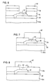
- a feature of this embodiment of the invention is that by using a positive photoresist and the and the above- described etchants, the polyimide layers can be etched as the positive photoresist is developed. In other words, the photoresist is patterned and openings are created in the underlying polyimide layers during the course of a single wet etch step. See Fig. 5.
- the positive photoresist 38 is removed using n-butyl acetate or any other solvent (e.g. iso-propyl alcohol or acetone) which removes photoresist without appreciably attacking underlaying polyamic acids such as polyimide.
- n-butyl acetate or any other solvent e.g. iso-propyl alcohol or acetone
- this removal step is not necessary, in that the photoresist could be removed as polyimide layer 36 is lifted off as described below. By removing the photoresist separately, lift-off can be carried out more efficiently.
- the polyimide layers are heated to approximately 200 C, which is sufficient to fully imidize (i.e. achieve at least 98% imidization) polyimide layer 34 and to imidize high-temperature polyimide layer 36 by an inconsequential amount (e.g. 2-5%).
- the apertures formed in the polyimide layers are briefly etched, using either plasma or wet etch techniques, in order to remove any impurities.
- a suitable wet etchant would be chromic-phosphoric acid, and a suitable atmosphere for plasma etching would be CF 4 or CF 4 + 0 2 . Again, while this step is not absolutely necessary, it contributes to the reliability of the overall process.
- a conductor layer 40 is then deposited.
- This layer e.g. a combination of chromium, copper and gold or titanium, copper and gold
- the substrate 10A should be heated to 200-280 ° C during deposition in order to minimize the defects in the pad metallurgy layer. Note that other metals (e.g. aluminum) could be used here.
- solder balls 42 are deposited on the remaining portions of conductor layer 40, using well known techniques (e.g. evaporating the solder through a metal mask), resulting in the structure as shown in Fig. 7.
- a wire bond metallurgy could be deposited on conductor layer 40, again using conventional techniques.
- the second embodiment of the invention as described above can be modified as follows.
- the process can be altered by eliminating the positive resist strip.
- TMAH or KOH solvents Immediately before the via holes are etched in order to remove impurities, briefly expose the structure to TMAH or KOH solvents for a time sufficient to etch back the sidewalls of the opening formed in high-temperature polyimide layer 36 without appreciably affecting the via holes in polyimide layer 34.
- the metal upon application of conductor layer 40, the metal will overflow the via holes in polyimide layer 34 by a controllable amount (i.e. the extent to which the sidewalls of the aperture in polyimide layer 36 were etched back).
- the process is then completed as described, resulting in a structure as shown in Fig. 8.
- both embodiments of the invention present a method by which high-temperature polyimide layers are used to form a lift-off structure without the need for a barrier layer.
- the first embodiment of the invention provides an efficient method of forming patterned interconnection layers
- the second embodiment of the invention provides an efficient method of providing an interconnection between the final metallization layer and the solder balls or wire bonds.
Landscapes
- Internal Circuitry In Semiconductor Integrated Circuit Devices (AREA)
- Drying Of Semiconductors (AREA)
Claims (11)
Applications Claiming Priority (2)
| Application Number | Priority Date | Filing Date | Title |
|---|---|---|---|
| US728072 | 1985-04-30 | ||
| US06/728,072 US4606998A (en) | 1985-04-30 | 1985-04-30 | Barrierless high-temperature lift-off process |
Publications (3)
| Publication Number | Publication Date |
|---|---|
| EP0200082A2 EP0200082A2 (de) | 1986-11-05 |
| EP0200082A3 EP0200082A3 (en) | 1988-11-17 |
| EP0200082B1 true EP0200082B1 (de) | 1992-07-08 |
Family
ID=24925304
Family Applications (1)
| Application Number | Title | Priority Date | Filing Date |
|---|---|---|---|
| EP86105142A Expired EP0200082B1 (de) | 1985-04-30 | 1986-04-15 | Hochtemperatur Abhebeverfahren ohne Zwischenschicht für eine strukturierte Zwischenverbindungsschicht |
Country Status (5)
| Country | Link |
|---|---|
| US (1) | US4606998A (de) |
| EP (1) | EP0200082B1 (de) |
| JP (1) | JPS61252648A (de) |
| CA (1) | CA1223089A (de) |
| DE (1) | DE3685906T2 (de) |
Families Citing this family (43)
| Publication number | Priority date | Publication date | Assignee | Title |
|---|---|---|---|---|
| IT1184535B (it) * | 1985-05-03 | 1987-10-28 | Gte Telecom Spa | Processo di ricavo di linee in film sottile |
| US4828964A (en) * | 1985-08-20 | 1989-05-09 | International Business Machines Corporation | Polyimide formulation for forming a patterned film on a substrate |
| US4890157A (en) * | 1986-01-31 | 1989-12-26 | Texas Instruments Incorporated | Integrated circuit product having a polyimide film interconnection structure |
| ZA87922B (en) * | 1986-02-28 | 1987-09-30 | Macdermid Inc | Photoresist stripper composition |
| US4943471A (en) * | 1986-05-20 | 1990-07-24 | Kanegafuchi Kagaku Kogyo Kabushiki Kaisha | Patterned thin film and process for preparing the same |
| US4886573A (en) * | 1986-08-27 | 1989-12-12 | Hitachi, Ltd. | Process for forming wiring on substrate |
| GB2212979A (en) * | 1987-12-02 | 1989-08-02 | Philips Nv | Fabricating electrical connections,particularly in integrated circuit manufacture |
| US4846929A (en) * | 1988-07-13 | 1989-07-11 | Ibm Corporation | Wet etching of thermally or chemically cured polyimide |
| GB2226991A (en) * | 1989-01-13 | 1990-07-18 | Ibm | Etching organic polymeric materials |
| US4911786A (en) * | 1989-04-26 | 1990-03-27 | International Business Machines Corporation | Method of etching polyimides and resulting passivation structure |
| US4961259A (en) * | 1989-06-16 | 1990-10-09 | Hughes Aircraft Company | Method of forming an interconnection by an excimer laser |
| US5006488A (en) * | 1989-10-06 | 1991-04-09 | International Business Machines Corporation | High temperature lift-off process |
| SE465193B (sv) * | 1989-12-06 | 1991-08-05 | Ericsson Telefon Ab L M | Foer hoegspaenning avsedd ic-krets |
| US5130229A (en) * | 1990-04-26 | 1992-07-14 | International Business Machines Corporation | Multi layer thin film wiring process featuring self-alignment of vias |
| DE4034868C2 (de) * | 1990-11-02 | 1995-02-16 | Itt Ind Gmbh Deutsche | Verfahren zur selektiven Metallabscheidung bei der Herstellung von Halbleiterbauelementen |
| DE69219998T2 (de) * | 1991-10-31 | 1997-12-18 | Sgs Thomson Microelectronics | Verfahren zur Entfernung von Polymeren aus Sacklöchern in Halbleitervorrichtungen |
| US5242864A (en) * | 1992-06-05 | 1993-09-07 | Intel Corporation | Polyimide process for protecting integrated circuits |
| DE69330603T2 (de) * | 1993-09-30 | 2002-07-04 | Consorzio Per La Ricerca Sulla Microelettronica Nel Mezzogiorno, Catania | Verfahren zur Metallisierung und Verbindung bei der Herstellung von Leistungshalbleiterbauelementen |
| US5798287A (en) * | 1993-12-24 | 1998-08-25 | Consorzio Per La Ricerca Sulla Microelettronica Nel Mezzogiorno | Method for forming a power MOS device chip |
| DE69321965T2 (de) * | 1993-12-24 | 1999-06-02 | Consorzio Per La Ricerca Sulla Microelettronica Nel Mezzogiorno, Catania | MOS-Leistungs-Chip-Typ und Packungszusammenbau |
| DE69321966T2 (de) * | 1993-12-24 | 1999-06-02 | Consorzio Per La Ricerca Sulla Microelettronica Nel Mezzogiorno, Catania | Leistungs-Halbleiterbauelement |
| US5597983A (en) * | 1994-02-03 | 1997-01-28 | Sgs-Thomson Microelectronics, Inc. | Process of removing polymers in semiconductor vias |
| US5503961A (en) * | 1994-11-02 | 1996-04-02 | International Business Machines Corporation | Process for forming multilayer lift-off structures |
| US5474956A (en) * | 1995-03-14 | 1995-12-12 | Hughes Aircraft Company | Method of fabricating metallized substrates using an organic etch block layer |
| JP2817664B2 (ja) * | 1995-04-24 | 1998-10-30 | 日本電気株式会社 | 半導体装置の製造方法 |
| US6410922B1 (en) | 1995-11-29 | 2002-06-25 | Konstantinos Evangelos Spartiotis | Forming contacts on semiconductor substrates for radiation detectors and imaging devices |
| GB2352084B (en) * | 1999-07-13 | 2002-11-13 | Simage Oy | Forming contacts on semiconductor substrates for radiation detectors and imaging devices |
| US6998711B1 (en) * | 1998-08-14 | 2006-02-14 | Micron Technology, Inc. | Method of forming a micro solder ball for use in C4 bonding process |
| US6136689A (en) * | 1998-08-14 | 2000-10-24 | Micron Technology, Inc. | Method of forming a micro solder ball for use in C4 bonding process |
| US6589712B1 (en) * | 1998-11-04 | 2003-07-08 | Yi-Ren Hsu | Method for forming a passivation layer using polyimide layer as a mask |
| US6878396B2 (en) * | 2000-04-10 | 2005-04-12 | Micron Technology, Inc. | Micro C-4 semiconductor die and method for depositing connection sites thereon |
| US6759275B1 (en) | 2001-09-04 | 2004-07-06 | Megic Corporation | Method for making high-performance RF integrated circuits |
| JP4085384B2 (ja) * | 2003-06-09 | 2008-05-14 | ミネベア株式会社 | 薄膜パターンの形成方法 |
| DE102005002550B4 (de) * | 2005-01-19 | 2007-02-08 | Infineon Technologies Ag | Lift-Off-Verfahren |
| US7553718B2 (en) * | 2005-01-28 | 2009-06-30 | Texas Instruments Incorporated | Methods, systems and structures for forming semiconductor structures incorporating high-temperature processing steps |
| CN1901162B (zh) | 2005-07-22 | 2011-04-20 | 米辑电子股份有限公司 | 连续电镀制作线路组件的方法及线路组件结构 |
| KR100633994B1 (ko) * | 2005-07-26 | 2006-10-13 | 동부일렉트로닉스 주식회사 | 반도체 소자의 웰 포토레지스트 패턴 및 그 형성 방법 |
| US20070036890A1 (en) * | 2005-08-12 | 2007-02-15 | Feng Zhong | Method of making a fuel cell component using a mask |
| US8697503B2 (en) * | 2006-08-10 | 2014-04-15 | Koninklijke Philips N.V. | Active matrix displays and other electronic devices having plastic substrates |
| US7862987B2 (en) * | 2007-11-20 | 2011-01-04 | International Business Machines Corporation | Method for forming an electrical structure comprising multiple photosensitive materials |
| CN110098108A (zh) * | 2018-01-31 | 2019-08-06 | 苏州锐材半导体有限公司 | 一种聚酰亚胺微掩膜的制作方法 |
| US12520425B2 (en) | 2020-04-30 | 2026-01-06 | Dujud Llc | Three-dimensional circuits with flexible interconnects |
| US11304303B2 (en) * | 2020-04-30 | 2022-04-12 | Dujud Llc | Methods and processes for forming electrical circuitries on three-dimensional geometries |
Family Cites Families (9)
| Publication number | Priority date | Publication date | Assignee | Title |
|---|---|---|---|---|
| US3985597A (en) * | 1975-05-01 | 1976-10-12 | International Business Machines Corporation | Process for forming passivated metal interconnection system with a planar surface |
| JPS55163860A (en) * | 1979-06-06 | 1980-12-20 | Toshiba Corp | Manufacture of semiconductor device |
| US4377115A (en) * | 1979-12-21 | 1983-03-22 | Kolze Bruce A | Furnace for burning particulate wood waste material |
| US4353778A (en) * | 1981-09-04 | 1982-10-12 | International Business Machines Corporation | Method of etching polyimide |
| US4451971A (en) * | 1982-08-02 | 1984-06-05 | Fairchild Camera And Instrument Corporation | Lift-off wafer processing |
| US4428796A (en) * | 1982-08-02 | 1984-01-31 | Fairchild Camera And Instrument Corporation | Adhesion bond-breaking of lift-off regions on semiconductor structures |
| JPS6018923A (ja) * | 1983-07-13 | 1985-01-31 | Hitachi Ltd | ポリイミド系樹脂層のテ−パエツチング方法 |
| US4523976A (en) * | 1984-07-02 | 1985-06-18 | Motorola, Inc. | Method for forming semiconductor devices |
| US4624740A (en) * | 1985-01-22 | 1986-11-25 | International Business Machines Corporation | Tailoring of via-hole sidewall slope |
-
1985
- 1985-04-30 US US06/728,072 patent/US4606998A/en not_active Expired - Lifetime
- 1985-11-19 CA CA000495660A patent/CA1223089A/en not_active Expired
-
1986
- 1986-01-29 JP JP61015985A patent/JPS61252648A/ja active Pending
- 1986-04-15 EP EP86105142A patent/EP0200082B1/de not_active Expired
- 1986-04-15 DE DE8686105142T patent/DE3685906T2/de not_active Expired - Fee Related
Also Published As
| Publication number | Publication date |
|---|---|
| US4606998A (en) | 1986-08-19 |
| JPS61252648A (ja) | 1986-11-10 |
| DE3685906T2 (de) | 1993-02-04 |
| EP0200082A2 (de) | 1986-11-05 |
| DE3685906D1 (de) | 1992-08-13 |
| CA1223089A (en) | 1987-06-16 |
| EP0200082A3 (en) | 1988-11-17 |
Similar Documents
| Publication | Publication Date | Title |
|---|---|---|
| EP0200082A2 (de) | Hochtemperatur Abhebeverfahren ohne Zwischenschicht für eine strukturierte Zwischenverbindungsschicht | |
| US4076575A (en) | Integrated fabrication method of forming connectors through insulative layers | |
| US4440804A (en) | Lift-off process for fabricating self-aligned contacts | |
| US4035276A (en) | Making coplanar layers of thin films | |
| US4152195A (en) | Method of improving the adherence of metallic conductive lines on polyimide layers | |
| EP0046525B1 (de) | Planar mehrlagige Metallisolationsstruktur mit einem Substrat, einem leitenden Verbindungsmuster und einer überlagerten Leiterstruktur und ein Verfahren zum Formen einer solchen Struktur | |
| US6936923B2 (en) | Method to form very a fine pitch solder bump using methods of electroplating | |
| JP3270909B2 (ja) | 絶縁層により覆われている複数の接合パッドが形成される半導体基板の表面を保護する方法 | |
| EP0355478B1 (de) | Lift-off-Prozess für Metallanschlüsse | |
| US4040891A (en) | Etching process utilizing the same positive photoresist layer for two etching steps | |
| US20030199159A1 (en) | Novel method for dual-layer polyimide processing on bumping technology | |
| JPH0795521B2 (ja) | 基板上にパターン付けした皮膜を形成する方法 | |
| EP0102281B1 (de) | Verfahren zum Zerbrechen von klebenden Bindemitteln für abhebbare Zonen für Halbleiterstrukturen | |
| US4062720A (en) | Process for forming a ledge-free aluminum-copper-silicon conductor structure | |
| US4029562A (en) | Forming feedthrough connections for multi-level interconnections metallurgy systems | |
| JP2000124265A (ja) | Icチップを支持基板に接合する方法 | |
| US5674780A (en) | Method of forming an electrically conductive polymer bump over an aluminum electrode | |
| JPH0766942B2 (ja) | 多層相互接続導体パターン製造方法 | |
| US5051811A (en) | Solder or brazing barrier | |
| US4745089A (en) | Self-aligned barrier metal and oxidation mask method | |
| JP3009032B2 (ja) | 半導体装置の製造方法 | |
| EP0420405A2 (de) | Integrierte Schaltung mit Verbindungen | |
| JP3446021B2 (ja) | 半導体装置のバンプ電極構造およびその形成方法 | |
| JP2509175B2 (ja) | 配線構造体の製造方法 | |
| JP2842405B2 (ja) | 半導体装置の製造方法 |
Legal Events
| Date | Code | Title | Description |
|---|---|---|---|
| PUAI | Public reference made under article 153(3) epc to a published international application that has entered the european phase |
Free format text: ORIGINAL CODE: 0009012 |
|
| AK | Designated contracting states |
Kind code of ref document: A2 Designated state(s): DE FR GB IT |
|
| PUAB | Information related to the publication of an a document modified or deleted |
Free format text: ORIGINAL CODE: 0009199EPPU |
|
| RA1 | Application published (corrected) |
Date of ref document: 19861210 Kind code of ref document: A2 |
|
| 17P | Request for examination filed |
Effective date: 19870224 |
|
| PUAL | Search report despatched |
Free format text: ORIGINAL CODE: 0009013 |
|
| AK | Designated contracting states |
Kind code of ref document: A3 Designated state(s): DE FR GB IT |
|
| 17Q | First examination report despatched |
Effective date: 19901221 |
|
| GRAA | (expected) grant |
Free format text: ORIGINAL CODE: 0009210 |
|
| AK | Designated contracting states |
Kind code of ref document: B1 Designated state(s): DE FR GB IT |
|
| PG25 | Lapsed in a contracting state [announced via postgrant information from national office to epo] |
Ref country code: IT Free format text: LAPSE BECAUSE OF FAILURE TO SUBMIT A TRANSLATION OF THE DESCRIPTION OR TO PAY THE FEE WITHIN THE PRE;WARNING: LAPSES OF ITALIAN PATENTS WITH EFFECTIVE DATE BEFORE 2007 MAY HAVE OCCURRED AT ANY TIME BEFORE 2007. THE CORRECT EFFECTIVE DATE MAY BE DIFFERENT FROM THE ONE RECORDED.SCRIBED TIME-LIMIT Effective date: 19920708 |
|
| REF | Corresponds to: |
Ref document number: 3685906 Country of ref document: DE Date of ref document: 19920813 |
|
| ET | Fr: translation filed | ||
| PGFP | Annual fee paid to national office [announced via postgrant information from national office to epo] |
Ref country code: GB Payment date: 19930324 Year of fee payment: 8 |
|
| PGFP | Annual fee paid to national office [announced via postgrant information from national office to epo] |
Ref country code: FR Payment date: 19930330 Year of fee payment: 8 |
|
| PGFP | Annual fee paid to national office [announced via postgrant information from national office to epo] |
Ref country code: DE Payment date: 19930428 Year of fee payment: 8 |
|
| PLBE | No opposition filed within time limit |
Free format text: ORIGINAL CODE: 0009261 |
|
| STAA | Information on the status of an ep patent application or granted ep patent |
Free format text: STATUS: NO OPPOSITION FILED WITHIN TIME LIMIT |
|
| 26N | No opposition filed | ||
| PG25 | Lapsed in a contracting state [announced via postgrant information from national office to epo] |
Ref country code: GB Effective date: 19940415 |
|
| GBPC | Gb: european patent ceased through non-payment of renewal fee |
Effective date: 19940415 |
|
| PG25 | Lapsed in a contracting state [announced via postgrant information from national office to epo] |
Ref country code: FR Effective date: 19941229 |
|
| PG25 | Lapsed in a contracting state [announced via postgrant information from national office to epo] |
Ref country code: DE Effective date: 19950103 |
|
| REG | Reference to a national code |
Ref country code: FR Ref legal event code: ST |