EP0200266A1 - Schaltung zur Erzeugung alternierender Komplementärsignale - Google Patents
Schaltung zur Erzeugung alternierender Komplementärsignale Download PDFInfo
- Publication number
- EP0200266A1 EP0200266A1 EP86200699A EP86200699A EP0200266A1 EP 0200266 A1 EP0200266 A1 EP 0200266A1 EP 86200699 A EP86200699 A EP 86200699A EP 86200699 A EP86200699 A EP 86200699A EP 0200266 A1 EP0200266 A1 EP 0200266A1
- Authority
- EP
- European Patent Office
- Prior art keywords
- stage
- gate
- circuit
- signals
- alternating
- Prior art date
- Legal status (The legal status is an assumption and is not a legal conclusion. Google has not performed a legal analysis and makes no representation as to the accuracy of the status listed.)
- Withdrawn
Links
- 230000000295 complement effect Effects 0.000 title claims abstract description 30
- 230000000630 rising effect Effects 0.000 claims abstract description 7
- 230000005669 field effect Effects 0.000 claims description 11
- JBRZTFJDHDCESZ-UHFFFAOYSA-N AsGa Chemical compound [As]#[Ga] JBRZTFJDHDCESZ-UHFFFAOYSA-N 0.000 claims description 5
- 230000010287 polarization Effects 0.000 claims description 2
- 230000009467 reduction Effects 0.000 claims description 2
- 230000007704 transition Effects 0.000 description 10
- 230000008901 benefit Effects 0.000 description 4
- 238000010586 diagram Methods 0.000 description 4
- 238000005516 engineering process Methods 0.000 description 4
- 229910001218 Gallium arsenide Inorganic materials 0.000 description 3
- 230000007547 defect Effects 0.000 description 2
- 235000021183 entrée Nutrition 0.000 description 2
- 238000004519 manufacturing process Methods 0.000 description 2
- 241001080024 Telles Species 0.000 description 1
- 239000008186 active pharmaceutical agent Substances 0.000 description 1
- 230000008859 change Effects 0.000 description 1
- 230000008878 coupling Effects 0.000 description 1
- 238000010168 coupling process Methods 0.000 description 1
- 238000005859 coupling reaction Methods 0.000 description 1
- 230000010354 integration Effects 0.000 description 1
- 230000035945 sensitivity Effects 0.000 description 1
Images
Classifications
-
- H—ELECTRICITY
- H03—ELECTRONIC CIRCUITRY
- H03K—PULSE TECHNIQUE
- H03K3/00—Circuits for generating electric pulses; Monostable, bistable or multistable circuits
- H03K3/02—Generators characterised by the type of circuit or by the means used for producing pulses
- H03K3/353—Generators characterised by the type of circuit or by the means used for producing pulses by the use, as active elements, of field-effect transistors with internal or external positive feedback
- H03K3/356—Bistable circuits
- H03K3/3562—Bistable circuits of the primary-secondary type
-
- H—ELECTRICITY
- H03—ELECTRONIC CIRCUITRY
- H03K—PULSE TECHNIQUE
- H03K3/00—Circuits for generating electric pulses; Monostable, bistable or multistable circuits
- H03K3/02—Generators characterised by the type of circuit or by the means used for producing pulses
- H03K3/027—Generators characterised by the type of circuit or by the means used for producing pulses by the use of logic circuits, with internal or external positive feedback
- H03K3/037—Bistable circuits
- H03K3/0372—Bistable circuits of the primary-secondary type
Definitions
- the invention relates to a circuit generating complementary alternative signals for constituting the input signals of a frequency divider by two.
- the invention also relates to such an alternating signal generator circuit with which is associated a frequency divider circuit by two.
- the invention finds its application in the realization of frequency divider circuit by two very wide band, that is to say typically between 40 MHz and 8 GHz.
- a circuit generating microwave signals is known from the publication IEEE Journal of Solid-State Circuits Vot. SC-18 (1983) June, p.373 and p.374.
- This circuit is composed of two field effect transistors, one of which receives the input signal on its gate and provides a first microwave signal on its drain, and the other of which receives the input signal on its source, its grid being polarized by a signal taken at the common point between a resistor and a diode placed between the DC supply voltage and the ground, and provides a second microwave signal complementary to the first on its drain.
- this clock generator circuit has slow transitions, that is to say not abrupt rising edges. This can be negligible in the frequency divider by two circuit presented in the cited publication. However, for the circuit envisaged in the present application at the frequency band 40 MHz-8 GHz, this signal generator must be absolutely discarded. Indeed at low frequencies, when the rising edge of the clock is not sufficiently abrupt, an indeterminacy is created between the high level and the low level of one of the stages of the divider, hindering a total loss of t 'information. On the other hand, at very high frequencies, the slowness of the transitions of the clock generator limits the higher operating frequency of the divider.
- this known circuit was produced in interfaced logic BFL, 'using field effect transistors in gallium arsenide, with charge desertion.
- the physicochemical properties of gallium arsenide indeed allow the production of integrated circuits operating at very high frequencies, and the charge-effect field effect transistors are relatively easy to produce.
- the enrichment field effect transistors whose technology is now satisfactory, are to date preferred because they are free from the defects inherent in charge-depletion transistors, and their consumption is about ten times less.
- circuits designed to be produced in a technology including charge desertion transistors cannot be transposed purely and simply in a technology including enrichment transistors - (normally blocked in absence of gate-source signal).
- these circuits operate under good conditions using charge-depletion transistors because the doors have significant logic excursions - (greater than 1V), the transfer of the voltage from one stage to the next being achieved by via diode level translator stages requiring the use of an additional DC supply voltage.
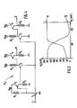
- this circuit is remarkable in that it consists of a first inverter circuit formed by an inverter stage and a follower stage, this first inverter circuit receiving the alternating input signal E and providing the complementary E of this alternating input signal, in that it further consists of two branches each formed by the succession of an inverter stage and a follower stage, the first branch receiving the alternating input signal E and supplying the alternating output signal H complementary, and the second branch receiving the complementary E of the input signal E and supplying the alternating output signal H, this second branch also being such that the source of the inverter transistor is polarized by the signal AC input, in that the elements of which it is formed cooperate so that the AC signals H and H have abrupt rising edges, and in that the signals H and H thus generated constitute the signals alternative input of a frequency divider organized into two stages, a master stage and a slave stage, providing two complementary outputs Q and Q and operating between very low frequencies and microwave frequencies.
- each master stage and each slave stage is formed by two multiplexing gates and in that each multiplexing gate consists of two NOR gates and an OU-CABLE gate and receives on the one hand the alternating signals H and H and on the other hand the looped-back signal from the output of the other multiplexing gate of the same stage, and the output signal of one multiplexing doors on the other floor.
- This circuit can also be remarkable in that it is produced using field effect transistors of the so-called enrichment type normally pinched in the absence of gate-source signal, in that it includes means for reducing the propagation time in the NOR gates, and in that, each NOR gate being formed of two transistors in parallel whose coupled sources are connected to ground, whose coupled drains are brought to the supply voltage continuous V DD through a load resistor, and the gates of which receive the door inputs, the means for reducing the propagation time in this NOR gate consist of the fact that the door output, which is available on the coupled drains, is transferred to the input of a so-called buffer stage composed of a transistor whose drain is brought directly to the DC supply V DD , and whose source is brought to ground through a resistor whose the value is chosen so that the input capacity of the buffer stage is low and thus the load resistance of the NOR gate is also low, which produces the desired reduction in the propagation time in this door.
- each OU-CABLE is formed by the union of the surces of the transistors of the buffer stages of the two NOR gates of a multiplexing gate and in that the bias resistance of these transistors d buffer stage is pooled to make only one, the output of the OU-CABLE then being in common between these sources and this resistance, so that the transit time in the divider is that of the sum of the transit time in two transistors and since 5 is the propagation time in a NOR gate, the maximum operating frequency f M of the frequency divider part is given by the relation:
- the circuit according to the invention therefore provides a double advantage.
- the transit time in the latter does not exceed the transit time in two transistors, which obviously improves the performance of this part of the circuit compared to the prior art where the transit time was that of three transistors because the OR function was performed by an additional transistor.
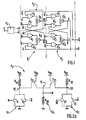
- the divider circuit therefore consists of two stages, a master stage P, and a slave stage P 2 .
- Each of these stages is formed by two complex gates called NOR-OR, OR multiplexing.
- the master is formed of a first multiplexing door comprising two NOR gates denoted G, and G 2 , and an OR gate denoted G s , and a second multiplexing gate comprising two NOR gates denoted G 3 and G 4 and an OR gate denoted G 6 .
- the slave is formed of a first multiplexing door comprising two NOR doors denoted G ', and G' 2 and an OR gate denoted G ' s , and a second multiplexing door comprising two NOR doors denoted G ' 3 and G' 4 and an OR gate denoted G ' 6 .
- the doors G, and G 4 of the mayor each receive the alternative input signal H.
- the door G receives, in addition the complementary output Q from the door G ' 6 of the slave, while the door G4 receives in in addition to the Q output from gate G ' 5 of the slave.
- Gates G 2 and G 3 of the master each receive the additional input signal H .
- the gate G 2 also receives the complementary M of the intermediate signal, coming from the gate G 6 of the master, while the gate G 3 also receives the intermediate signal M coming from the gate G s of the master.
- the OR doors G 5 and G 6 of the master in fact only carry out the wiring of the outputs of the doors G, and G 2 on the one hand, and G 3 and G4 on the other hand. These doors G 5 and G 6 called "OU-CABLE" therefore have no propagation time.
- the gates G ', and G' ⁇ of the slave each receive the complementary H of the alternative input signal.
- the gate G ' also receives the intermediate signal M from the gate G 5 of the master, while the gate G' 4 receives the complementary M of the intermediate signal, from the gate G6 of the mayor.
- the doors G ' 2 and G' 3 of the slave each receive the alternative input signal H.
- the door G ' 2 also receives the complementary signal Q from gate G ' 6 of the slave, while gate G' 3 , also receives the output signal Q from gate G ' 5 of the slave.
- the doors G ' 5 and G' 6 of the slave are formed respectively by the wiring of the outputs of the doors G ', and G' 2 on the one hand, and G ' 3 and G' 4 on the other hand, so that they form OU-CABLES quite similar to the doors G s and G 6 of the master.
- this circuit is formed of field effect transistors, for example of gallium arsenide (GaAs), of the so-called enrichment type, that is to say normally blocked at gate voltage -source zero (Normally-OFF).
- GaAs gallium arsenide
- Normally-OFF gate voltage -source zero
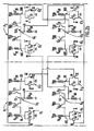
- the multiplexing gate including two NOR gates such as G, and G2 and an OR-CABLE such as G s is provided according to the diagram in Figure 2a.
- this multiplexing gate P 3 therefore comprises a first NOR gate, for example G 1 , formed of two transistors T ,, and T 12 mounted in parallel and charged on a resistor R, o , and a second NOR gate, for example G2, formed of two transistors T 21 and T u mounted in parallel and loaded on a resistor R 20
- the output signal from these gates is available at nodes 10 and 20 respectively and is reported on the gates of the transistors T 13 and T 23 , the drains of which are brought directly to the continuous supply V DD and the sources of which are coupled and brought to ground via a resistor R so .
- the node 15 for coupling the sources of the transistors T 13 and T 23 constitutes the OU-CABLE function of the gate G s for example.
- the value of the resistance R so is chosen so that the input capacity of the transistor of the buffer stage is low, and so that the compatibility of the levels is nevertheless preserved.
- a multiplexing gate P 3 as shown in FIG. 2a provides the complex function as an output (for example for the doors G ,, G 2 and G 5 ):
- FIG. 2b represents the complete frequency divider by two circuit according to the invention, produced using four multiplexing doors.
- Figure 3 shows the timing diagram for the operation of this circuit. Based on Figure 1, and assuming that the initial state of the system at time t o is that given in Table 1: then, during the first transition, at time t , the slave closes - there is storage - and the intermediate signal M goes to the high level exactly at the same time as its complement M goes to the low level. This state of the intermediate signal M and of its complement M is reached after a time noted ⁇ after the instant t ,.
- each stage, master or slave alternately passes from a storage phase to an acquisition phase and vice versa.
- the transistor T 23 must compensate a gate-source voltage of the order of 0.6 V before becoming sufficiently conducting to impose the high level on the node 15. This point 15 will therefore react initially to T 13 and its level will start to fall.
- This circuit P4 is shown in Figure 4.
- the inverter stages are formed by the transistor T 3 and the resistor R 3 on the one hand, and the transistor T ' 3 and the resistor R' 3 on the other hand.
- the follower stages are formed by the transistor T4 and the resistor R4 on the one hand, and by the transistor T'4 and the resistor R ' 4 on the other hand.
- the gate voltage of the follower transistor T 3 due to the fact that it is a field effect transistor and that the gate current is not not zero, then the gate bias circuit of this transistor must be specially studied.
- the gate of transistor T 3 is polarized with the inverse of the input signal E, the signal E itself being applied to the source of transistor T 3 .
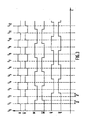
- FIG. 5 shows the transfer curves of this signal-generating circuit P 4 , under the conditions of embodiment set out in table II.
- the excursion is around 500 mV at output - (V s ) for 100 mV at input (V E ), in the maximum gain zone.
- table II gives the values of the gate width of the transistors, and the values of the resistances of the circuits as shown in FIG. 2a on the one hand and in FIG. 4 on the other go.
Landscapes
- Manipulation Of Pulses (AREA)
- Logic Circuits (AREA)
Applications Claiming Priority (2)
| Application Number | Priority Date | Filing Date | Title |
|---|---|---|---|
| FR8506408A FR2581267A1 (fr) | 1985-04-26 | 1985-04-26 | Diviseur de frequence par deux |
| FR8506408 | 1985-04-26 |
Publications (1)
| Publication Number | Publication Date |
|---|---|
| EP0200266A1 true EP0200266A1 (de) | 1986-11-05 |
Family
ID=9318731
Family Applications (1)
| Application Number | Title | Priority Date | Filing Date |
|---|---|---|---|
| EP86200699A Withdrawn EP0200266A1 (de) | 1985-04-26 | 1986-04-23 | Schaltung zur Erzeugung alternierender Komplementärsignale |
Country Status (2)
| Country | Link |
|---|---|
| EP (1) | EP0200266A1 (de) |
| FR (1) | FR2581267A1 (de) |
Cited By (2)
| Publication number | Priority date | Publication date | Assignee | Title |
|---|---|---|---|---|
| GB2573795A (en) * | 2018-05-17 | 2019-11-20 | Pragmatic Printing Ltd | AND gates and clock dividers |
| GB2611882A (en) * | 2018-05-17 | 2023-04-19 | Pragmatic Printing Ltd | AND gates and clock dividers |
Citations (3)
| Publication number | Priority date | Publication date | Assignee | Title |
|---|---|---|---|---|
| FR2423818A1 (fr) * | 1978-04-17 | 1979-11-16 | Labo Cent Telecommunicat | Generateur de signaux d'horloge sans recouvrement |
| EP0075915A2 (de) * | 1981-09-30 | 1983-04-06 | Kabushiki Kaisha Toshiba | Logische Schaltung gespeist durch nur eine Spannung |
| EP0098203A1 (de) * | 1982-06-29 | 1984-01-11 | Thomson-Csf | Mit Gleichspannung bis 10 GHz arbeitende logische Kippschaltung und diese enthaltender Frequenzteiler |
-
1985
- 1985-04-26 FR FR8506408A patent/FR2581267A1/fr not_active Withdrawn
-
1986
- 1986-04-23 EP EP86200699A patent/EP0200266A1/de not_active Withdrawn
Patent Citations (3)
| Publication number | Priority date | Publication date | Assignee | Title |
|---|---|---|---|---|
| FR2423818A1 (fr) * | 1978-04-17 | 1979-11-16 | Labo Cent Telecommunicat | Generateur de signaux d'horloge sans recouvrement |
| EP0075915A2 (de) * | 1981-09-30 | 1983-04-06 | Kabushiki Kaisha Toshiba | Logische Schaltung gespeist durch nur eine Spannung |
| EP0098203A1 (de) * | 1982-06-29 | 1984-01-11 | Thomson-Csf | Mit Gleichspannung bis 10 GHz arbeitende logische Kippschaltung und diese enthaltender Frequenzteiler |
Non-Patent Citations (3)
| Title |
|---|
| ELECTRONICS, vol. 53, no. 22, octobre 1980, pages 76-78, New York, US; K. DREYFACK: "Gallium arsenide to yield 5-GHz divider" * |
| IEE PROCEEDINGS-I, vol. 127, no. 5, partie 1, octobre 1980, pages 287-295, Stevenage, GB; "G. NUZILLAT et al.: "Low pinch-off voltage f.e.t. logic (l.p.f.l.): l.s.i. oriented logic approach using quasinormally off GaAs m.e.s.f.e.t.s." * |
| IEEE JOURNAL OF SOLID-STATE CIRCUITS, vol. SC-18, no. 3, juin 1983, pages 369-376, New York, US; M. ROCCHI et al.: "GaAs digital dynamic IC's for applications up to 10 GHz" * |
Cited By (6)
| Publication number | Priority date | Publication date | Assignee | Title |
|---|---|---|---|---|
| GB2573795A (en) * | 2018-05-17 | 2019-11-20 | Pragmatic Printing Ltd | AND gates and clock dividers |
| US11316518B2 (en) | 2018-05-17 | 2022-04-26 | Pragmatic Printing Ltd. | AND gates and clock dividers |
| GB2573795B (en) * | 2018-05-17 | 2023-01-11 | Pragmatic Printing Ltd | AND gates and clock dividers |
| US11575380B2 (en) | 2018-05-17 | 2023-02-07 | Pragmatic Printing Ltd. | And gates and clock dividers |
| GB2611882A (en) * | 2018-05-17 | 2023-04-19 | Pragmatic Printing Ltd | AND gates and clock dividers |
| GB2611882B (en) * | 2018-05-17 | 2023-07-05 | Pragmatic Printing Ltd | AND gates and clock dividers |
Also Published As
| Publication number | Publication date |
|---|---|
| FR2581267A1 (fr) | 1986-10-31 |
Similar Documents
| Publication | Publication Date | Title |
|---|---|---|
| EP0645888B1 (de) | Digitale Verzögerungsleitung | |
| US6888394B2 (en) | Voltage level shifting circuit with improved switching speed | |
| WO1991012666A1 (fr) | Circuit verrouille en phase et multiplieur de frequence en resultant | |
| FR2668669A1 (fr) | Circuit et procede de generation de signaux de temps. | |
| EP0626754A1 (de) | Verfahren und Einrichtung zur Amplitudenmodulierung eines Radiofrequenzsignals | |
| EP0130645B1 (de) | Frequenzteiler durch zwei | |
| FR2527801A1 (fr) | Appareil de telecommande a commande pluri-directionnelle | |
| FR2668668A1 (fr) | Generateur de tension de substrat pour un dispositif a semiconducteurs. | |
| EP0194195B1 (de) | Statische bistabile Kippschaltung in CMOS-Technologie | |
| FR2760152A1 (fr) | Demultiplicateur de frequence a double module | |
| EP0194177B1 (de) | Teilnehmerschnittstellenschaltung mit Überwachungsbetrieb bei verringerter Speisung | |
| FR2543379A1 (fr) | Dispositif de demodulation directe en hyperfrequence et chaine de reception hyperfrequence comportant un tel dispositif | |
| BE897171A (fr) | Dispositif d'asservissement en frequence d'une horloge sur un signal exterieur de frequence moyenne tres precise mais comportant une gigue importante, | |
| EP0549043B1 (de) | Integrierte Schaltung mit einem Verstärker mit variabler Verstärkung | |
| EP0200266A1 (de) | Schaltung zur Erzeugung alternierender Komplementärsignale | |
| FR2530890A1 (fr) | Commande de declenchement de convertisseur avec compensation pour retard variable de commutation | |
| FR2792459A1 (fr) | Dispositif a semiconducteur ayant un transistor mis | |
| EP0246135B1 (de) | Phasen- und Frequenzdetektor und seine Anwendung in einer Phasenregelschleife | |
| FR2639489A1 (fr) | Dispositif interrupteur de puissance, notamment pour convertisseur de frequence | |
| EP0347985A1 (de) | Allpasstyp-Schaltung für ultrahohe Frequenzen | |
| EP0187584B1 (de) | Logisches Koinzidenztor und dieses verwendende logische sequentielle Schaltungen | |
| FR2573939A1 (fr) | Circuit multiplexeur de signaux integre a quatre voies d'entree | |
| FR2718903A1 (fr) | Circuit à retard réglable. | |
| FR2503486A1 (fr) | Circuit de commutation a basculeur | |
| FR2913807A1 (fr) | Echantillonneur-bloqueur protege contre des parasites de commutation |
Legal Events
| Date | Code | Title | Description |
|---|---|---|---|
| PUAI | Public reference made under article 153(3) epc to a published international application that has entered the european phase |
Free format text: ORIGINAL CODE: 0009012 |
|
| AK | Designated contracting states |
Kind code of ref document: A1 Designated state(s): CH DE FR GB IT LI NL |
|
| PUAB | Information related to the publication of an a document modified or deleted |
Free format text: ORIGINAL CODE: 0009199EPPU |
|
| PUAF | Information related to the publication of a search report (a3 document) modified or deleted |
Free format text: ORIGINAL CODE: 0009199SEPU |
|
| R17D | Deferred search report published (corrected) |
Effective date: 19861210 |
|
| RA1 | Application published (corrected) |
Date of ref document: 19861210 Kind code of ref document: A1 |
|
| 17P | Request for examination filed |
Effective date: 19870505 |
|
| 17Q | First examination report despatched |
Effective date: 19890302 |
|
| RAP1 | Party data changed (applicant data changed or rights of an application transferred) |
Owner name: N.V. PHILIPS' GLOEILAMPENFABRIEKEN Owner name: LABORATOIRES D'ELECTRONIQUE PHILIPS |
|
| STAA | Information on the status of an ep patent application or granted ep patent |
Free format text: STATUS: THE APPLICATION IS DEEMED TO BE WITHDRAWN |
|
| 18D | Application deemed to be withdrawn |
Effective date: 19890913 |
|
| RIN1 | Information on inventor provided before grant (corrected) |
Inventor name: DELHAYE, ETIENNE Inventor name: ROCCHI, MARC |