EP0200300A1 - Nichtzerstörendes Auslesen eines latenten elektrostatischen Bildes welches auf isolierendem Material gebildet wurde - Google Patents
Nichtzerstörendes Auslesen eines latenten elektrostatischen Bildes welches auf isolierendem Material gebildet wurde Download PDFInfo
- Publication number
- EP0200300A1 EP0200300A1 EP86301228A EP86301228A EP0200300A1 EP 0200300 A1 EP0200300 A1 EP 0200300A1 EP 86301228 A EP86301228 A EP 86301228A EP 86301228 A EP86301228 A EP 86301228A EP 0200300 A1 EP0200300 A1 EP 0200300A1
- Authority
- EP
- European Patent Office
- Prior art keywords
- semiconductor
- insulator
- light
- reference electrode
- layer
- Prior art date
- Legal status (The legal status is an assumption and is not a legal conclusion. Google has not performed a legal analysis and makes no representation as to the accuracy of the status listed.)
- Granted
Links
Images



Classifications
-
- G—PHYSICS
- G01—MEASURING; TESTING
- G01T—MEASUREMENT OF NUCLEAR OR X-RADIATION
- G01T1/00—Measuring X-radiation, gamma radiation, corpuscular radiation, or cosmic radiation
- G01T1/16—Measuring radiation intensity
- G01T1/28—Measuring radiation intensity with secondary-emission detectors
-
- G—PHYSICS
- G01—MEASURING; TESTING
- G01R—MEASURING ELECTRIC VARIABLES; MEASURING MAGNETIC VARIABLES
- G01R29/00—Arrangements for measuring or indicating electric quantities not covered by groups G01R19/00 - G01R27/00
- G01R29/24—Arrangements for measuring quantities of charge
-
- G—PHYSICS
- G01—MEASURING; TESTING
- G01R—MEASURING ELECTRIC VARIABLES; MEASURING MAGNETIC VARIABLES
- G01R31/00—Arrangements for testing electric properties; Arrangements for locating electric faults; Arrangements for electrical testing characterised by what is being tested not provided for elsewhere
- G01R31/26—Testing of individual semiconductor devices
- G01R31/265—Contactless testing
- G01R31/2656—Contactless testing using non-ionising electromagnetic radiation, e.g. optical radiation
-
- G—PHYSICS
- G01—MEASURING; TESTING
- G01T—MEASUREMENT OF NUCLEAR OR X-RADIATION
- G01T1/00—Measuring X-radiation, gamma radiation, corpuscular radiation, or cosmic radiation
- G01T1/16—Measuring radiation intensity
- G01T1/24—Measuring radiation intensity with semiconductor detectors
- G01T1/246—Measuring radiation intensity with semiconductor detectors utilizing latent read-out, e.g. charge stored and read-out later
-
- G—PHYSICS
- G03—PHOTOGRAPHY; CINEMATOGRAPHY; ANALOGOUS TECHNIQUES USING WAVES OTHER THAN OPTICAL WAVES; ELECTROGRAPHY; HOLOGRAPHY
- G03G—ELECTROGRAPHY; ELECTROPHOTOGRAPHY; MAGNETOGRAPHY
- G03G15/00—Apparatus for electrographic processes using a charge pattern
-
- G—PHYSICS
- G03—PHOTOGRAPHY; CINEMATOGRAPHY; ANALOGOUS TECHNIQUES USING WAVES OTHER THAN OPTICAL WAVES; ELECTROGRAPHY; HOLOGRAPHY
- G03G—ELECTROGRAPHY; ELECTROPHOTOGRAPHY; MAGNETOGRAPHY
- G03G15/00—Apparatus for electrographic processes using a charge pattern
- G03G15/054—Apparatus for electrographic processes using a charge pattern using X-rays, e.g. electroradiography
-
- G—PHYSICS
- G03—PHOTOGRAPHY; CINEMATOGRAPHY; ANALOGOUS TECHNIQUES USING WAVES OTHER THAN OPTICAL WAVES; ELECTROGRAPHY; HOLOGRAPHY
- G03G—ELECTROGRAPHY; ELECTROPHOTOGRAPHY; MAGNETOGRAPHY
- G03G15/00—Apparatus for electrographic processes using a charge pattern
- G03G15/22—Apparatus for electrographic processes using a charge pattern involving the combination of more than one step according to groups G03G13/02 - G03G13/20
- G03G15/221—Machines other than electrographic copiers, e.g. electrophotographic cameras, electrostatic typewriters
-
- G—PHYSICS
- G03—PHOTOGRAPHY; CINEMATOGRAPHY; ANALOGOUS TECHNIQUES USING WAVES OTHER THAN OPTICAL WAVES; ELECTROGRAPHY; HOLOGRAPHY
- G03G—ELECTROGRAPHY; ELECTROPHOTOGRAPHY; MAGNETOGRAPHY
- G03G5/00—Recording-members for original recording by exposure, e.g. to light, to heat or to electrons; Manufacture thereof; Selection of materials therefor
-
- G—PHYSICS
- G03—PHOTOGRAPHY; CINEMATOGRAPHY; ANALOGOUS TECHNIQUES USING WAVES OTHER THAN OPTICAL WAVES; ELECTROGRAPHY; HOLOGRAPHY
- G03G—ELECTROGRAPHY; ELECTROPHOTOGRAPHY; MAGNETOGRAPHY
- G03G5/00—Recording-members for original recording by exposure, e.g. to light, to heat or to electrons; Manufacture thereof; Selection of materials therefor
- G03G5/02—Charge-receiving layers
Definitions
- the present invention relates generally to an apparatus and method for the nondestructive readout of a latent electrostatic image formed on an insulating material. More particularly, the present invention is concerned with a method and apparatus for reading out the location and magnitude of accumulated charges (surface density of electrostatic charges) on a sheet or layer of insulating material which involves producing a surface depletion layer related to the accumulated charges on a sheet or layer of semiconducting material by induction and then determining the location and magnitude of the accumulated charges on the semiconductor material using the surface photovoltage effect.
- accumulated charges surface density of electrostatic charges
- the invention is especially useful in reading out a latent electrostatic image formed on an insulator by irradiation with X-rays but is not exclusively limited to electrostatic images formed by that type of radiation.
- electrostatic charges are unwanted and undesirable.
- accumulation of electrostatic charges i.e..static electricity
- electrostatic charge is usually determined from measurements of the electro- static potential on a surface. This can be done, for instance, by using an electrometer (high input impedance voltmeter) to measure the ac signal induced on a reference electrode. The ac signal may be generated in this method by periodically introducing an electrical shield into the space between the reference electrode and the surface under measurement.
- the electrometric method is nondestructive and allows for measurement of a magnitude of electrostatic charge.
- the determination of the distribution of charge requires slow and cumbersome mechanical scanning of the studied surface with a-small aperture reference electrode or the use of an array of electrodes.
- vidicon tube a charge distribution pattern is stored in a seniconductor target. The distribution of charge is determined by measuring the variation of electron beam current when the target is scanned by an electron beam.
- the charge distribution on a xerographic plate (i.e. the latent electrostatic image formed on the xerographic plate) is determined from the distribution of toner particles which are attracted to the xerographic plate by the charges during the development process.
- the photovoltaic response of the semiconductor InSb has been used for determination of the charge distribution induced in the semiconductor by an electromagnetic radiation. This is described by R. J. Phelen, Jr., and J. 0. Dimmock, in an article entitled, "Imaging and Storage with a Uniform MOS Structure", Applied Physics Letters, Vo. 22, No. 11, pp. 359-361, 1967.
- the image projected on a uniform MOS structure (a semitransparent metal film - oxide layer - InSb sandwich) modified the surface depletion region in the semiconductor.
- the charge stored in the depletion layer was determined by measuring the photovoltaic response resulting from saturation of this layer by a "reading" photon beam.
- the few micron thick depletion layer is the only active structure.
- the general conclusion of studies made to date is the existance of a correlation between the local magnitude of charge in the depletion layer at the semiconductor surface and the ac surface photovoltage.
- the ac surface photovoltage is defined herein as the variations of the surface potential induced by a photon beam which is intensity modulated, either periodically or not periodically. This photon beam may cause the generation of carriers at the front surface in the depletion region, or, when illuminated from the back (opposite side) in the bulk and diffusion (migration) of the carriers toward the depletion region
- U.S. Patent 3,859,527 to G. W. Luckey there is disclosed an apparatus and method for recording images on recording mediums which images correspond to higb energy radiation patterns.
- a temporary storage medium such as an infrared- stimulable phosphor or thermoluminescent material, is exposed to an incident pattern of high energy radiation.
- a tide intervals after exposure a small area beam of long wavelength radiation or heat scans the screen to release the stored energy as light.
- An appropriate sensor receives the light emitted by the screen and produces electrical energy in accordance with the light received.
- the information carried by the electrical energy is transformed into a recorded image by scanning an information storage medium with a light beam which is intensity modulated in accordance with the electrical energy.
- Articles of interest concerning gas ionography sometimes referred to as electron radiology, wherein X-ray photons are absorbed in a high-pressure gas between the parallel plates of an ion chamber and the ions produced are collected on an insulating foil covering one of the plates include "Efficiency and Resolu t-ion of Ionography in Diagnostic Radiology” by A. Campbell, D. Plewes and H. E. Johns in Medical Physics, Vol. 1, No. 1, 1974, pages 1-10; "Gas Ionization Methods of Electrostatic Image Formation in Radiography” by H. E. Hohns etc.,British Journal of Radiology, September , 1974, pages 319-329; "Charging Characteristics of Ionographic Latent Images", B. G.
- a method of reading out a latent electrostatic image formed on or at the surface of a sheet or layer of insulating material comprises providing a sheet or layer of semiconducting material in relatively close proximity to the insulating material so as to produce by induction a surface depletion layer at the : surface of a sheet or layer of semiconducting material and then measuring the ac surface photovoltage on the semiconducting material which is produced when the semiconducting material is scanned with an intensity modulated beam of light of appropriate wavelength.
- An apparatus for reading out accumulated charges in a sheet or layer of insulating material includes a sheet or layer of semiconducting material, a reference electrode, a light source, focussing optics, a scanner and amplifying electronics.
- the present invention is directed to (I) an apparatus for reading out the location and magnitude (or more exactly surface distribution) of the charges accumulated in a sheet or layer of insulating material and (II) a method of reading out a charge distribution pattern in a sheet or layer of an insulating material.
- the main parts of the apparatus are (1) a readout device, (2) a reference electrode, (3) an illumination system, (4) a scanner and (5) an electronic detection system.
- the readout device includes a sheet or layer of semiconductor material.
- the illumination system includes a light source focusing optics and a light modulator.
- the readout device may be attached to or be separated from the insulating material.
- the semiconductor material which may be in the form of either a sheet (wafer) or a layer (film) is provided with an . electrical contact on its back or side surface.
- the front surface of the semiconductor may be left uncovered or, for electrical protection, may be covered with a protective insulating layer.
- the semiconducting materials which may be used are crystalline, polycrystalline or amorphous silicon or alloys of silicon.
- the protective insulating layer may be, for example, silicon oxide or silicon nitride.
- the conductive reference electrode Positioned some distance from and in front of the front side of the semiconductor is the conductive reference electrode.
- the semiconductor may be illuminated (i.e. scanned) with light from the illumination system from either the front side through the reference electrode or from the back side.
- both the reference electrode and the protective insulating material must be transparent for the light being used, and in the case of illumination from the back side, the back electrical contact and any support or substrate for the semiconductor must be transparent to the light being used.
- front illumination the light of photon energy exceeding the band gap of semiconductor is .preferred for reason of high efficiency.
- the photon energy should be comparable to the energy gap, so that it will penetrate the semiconductor close enough to the front surface to provide carriers in the depletion layer.
- the insulating material (insulator) carrying the charge distribution which is to be sensed is much thinner than the gap between the semiconductor and reference electrode and in another embodiment, the thickness of the insulating material is comparable to the gap.
- the body of insulating material whose accumulated charge pattern is to be measured is placed so that its distance from the semiconductor is much smaller than the distance from the reference electrode.
- this insulating material may even be attached to the front surface of the semiconductor for instance by deposition over the protective, insulating layer.
- the effect of charge migration across the insulator can be determined by measuring the total charge accumulated in the insulator after removing charge which remained on the surface of the insulator opposite to the semiconductor. Such charge might be removed using a brush or an ac corona as practiced in xerography.
- the invention may also be used to measure the charge deposited directly on a layer of insulating material (e.g. protective insulator) formed by any means, such as deposition, on the semiconductor.
- a layer of insulating material e.g. protective insulator
- the deposition of charges may be produced by irradiation with X-rays of a gas., such as air, xenonor freon.
- the semiconductor is placed close to one side of the layer or plate of insulating material and the reference conductive electrode is located close to the opposite side of layer or plate of insulting material. If the charge is formed on one side of this insulating layer and then, as in the xerographic process, migrates in certain locations to the opposite surface, the charge located on the surface of the insulator that is close to the conductive reference electrode will be neutralized by the charge in the reference electrode and only the charge located at the surface neighboring the semiconductor will induce opposite charge in the semiconductor. In this case, the method of this invention will allow for determination of charge density pattern at one surface only, namely that surface located close to the semiconductor, and hence will allow for determination of the effect of charge migration in the insulator.
- the insulator under measurement should be transparent (or semitransparent) for the light used and the light used must not cause any charge redistribution in this insulator. This is not required in the case of back illumination providing that this illumination does not penetrate into the insulator under measurement.
- Sensing of the electrostatic charge accummulated in the insulating material according to the method of this invention requires the presence of a depletion layer in the semiconductor.
- a protective insulating layer that is either precharged (by external means) or with an appropriate charge built into it.
- the charge accumulated in the insulator under measurement will only modify the pre-established depletion layer.
- the presence of a depletion layer may also be achieved by the use of the semiconductor of the appropriate type of conductiveity allowing for formation of the depletion layer due to induced charge.
- an n-type semiconductor should be used for sensing negative charge and p-type for sensing positive charge.
- the charge build-up in the semiconductor surface (interface) states should be low enough to allow for modification of the depletion layer due to charge induced in the semiconductor.
- the output electrical signal produced in reading out the accumulated charges on the semiconductor is generated by the intensity modulated illumination in the charge sensitive part of the readout apparatus i.e. between the semiconductor and the reference electrode.
- the intensity modulated illumination in the charge sensitive part of the readout apparatus i.e. between the semiconductor and the reference electrode.
- different combination of the scanning mode and modulation can be used.
- scan the light may be modulated periodically (for example sinusoidally) or may be not modulated.
- the unmodulated light will in reality behave like pulse modulation since each area element is illuminated only for a short time.
- the probe In the voltage mode, the probe operates with a high input impedance electronic detection system. In the current mode, the input impedance of the electronic system is lower than the output impendance of the semiconductor-reference electrode system. In the voltage mode, the time constant of the probe ; including input of the electronic detection system should be longer than the period (or effective pulse length) of light modulation but should be short enough to allow for charging of the semiconductor (formation of the depletion layer). The time constants between seconds and milliseconds should be adequate.
- FIG. 1 there is shown an enlarged cross-sectional view of an insulator IM on which a latent electrostatic image may be formed (by any known means, not shown) and, a readout device 11 and a reference electrode 12 according to one embodiment of the invention.
- Readout device 11 includes a semiconductor plate 13 which is covered on its top or front surface 14 with a layer 15 of transparent protective insulating material.
- the protective insulating layer 15 serves as an electrical protection (blocking contact) against injection of charges from the semiconductor 13 into the body of insulating material IM whose electrostatic charge distribution is to be read out
- Reference electrode 12 is disposed above and spaced apart from semiconductor 13.
- the body of insulating material IM on which the electrostatic charge to be measured is formed is disposed in the space between semiconductor 13 and the reference electrode 12.
- Reference electrode 12 comprises an optically transparent conductive layer 17 (or a conductor layer divided into sectors - e.g. stripes) on a transparent substrate 18.
- reference electrode 12 may comprise a conductive wire cloth.
- Semiconductor plate 13 is electrically connected to a lead 19 through an electrical contact 21, which is in the form of a layer, on the back side 20 of semiconductor plate 13.
- Another electrical lead 23 is connected to conductive layer 17 of reference electrode 12.
- Readout device 11 may be illuminated (scanned) from the front (top) through the reference electrode 12 as shown by arrow A.
- a crystalline silicon wafer was used as the semiconductor plate 13. Both n-type and p-type silicon were used and tested. N-type silicon wafers were single crystal Czochralski or (111) orientation and resistivity in the range of to 7 ohms cm. P-type silicon were also single crystals Czochralski or (111) orientation and resistivity in the range of 7 to 14 ohms-cm. A 1000 to 3000 A silicon oxide overlayer was used as a protective insulator.
- the semiconductor 13 instead of using single crystal silicon, other possible materials which may be used for the semiconductor 13 are, for example, microcrystalline silicon, amorphous (hydrogenetad or nate) silicon and silicon-germanium alloys. These materials, as will be explained later, should be better for the construction of the readout device because the lifetime of minority carriers in these materials is shorter then in single crystals.
- the polycrystalline, microcrystalline and amorphous materials may also be produced in larger sizes than crystal wafers.
- the possible choices for the protective insulating layer 15 include silicon oxide (SiO 2 ) and silicon nitride (Si 3 N 4 ) deposited or formed by chemical reaction (e.g/ oxidation) and N-type or P-type amorphous silicon with silicon nitride.
- the reference electrode 12 used in the constructed embodiment was a stainless steel wire cloth with number of meshes per linear inch in the range of 150 x 150 to 400 x 400 and with openings in the range of 0.1 to 0.04 mm respectively. Some tests were also performed using indium tin oxide (ITO) films deposited over the surface of glass facing the semiconductor 13. Reference electrode 13 was separated from the semiconductor 13 by a distance d of about 0.5 mm or less. This distance d, depending on the electronics and type of application, may be enlarged up to several millimeters.
- ITO indium tin oxide
- the light sources used for illuminating the semiconductor in the constructed embodiments of the invention were light emitting diodes (LED) emitting light at the 585 and 700 nanometers (nm) and He-Ne (633 nm 15 nW) and diode (820 nm, 10 mW) lasers.
- LED light emitting diodes
- He-Ne 633 nm 15 nW
- diode 820 nm, 10 mW
- Readout device 11 was illuminated from the top, as shown by arrow A.
- Contact 21 may be in the form of a spot rather than a layer and may be on the side of semiconductor 13 rather than the back of semiconductor 13.
- Semiconductor 13 may also be illuminated from the back (i.e. bottom) as shown by arrow B. This latter configuration, however, requires that the substrate on which the semiconductor is formed (if semiconductor 13 is only a layer) be optically
- the wavelength of the exciting light must be matched to the band gap of the semiconductor 13 in such a way that generation of carriers in the semiconductor 13 happens close enough to the front (i.e. top), active surface of the semiconductor 13.
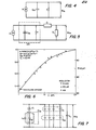
- Fig. 2 shows the distribution between semiconductor 13 and reference electrode 12 of the charge induced by a negative charge accumulated in a thin layer insulator IM T which is placed between semiconductor 13 and reference electrode 12.
- MOS metal-oxide- semi-conductor
- the present invention involves the determination of the charge accumulated in the insulating layer IM by measuring charge induced in semiconductor 13. Therefore, as follows from the above equations, the charge to be determined should be located close to semiconductor 13 and far from reference electrode 12 or at least all distances should be precisely known. Some of the possible configurations of insulator IM are shown in Figs. 3a, 3b and 3c.
- an insulator IM in the form of a thin insulating film is located relatively close to the semiconductor 13 (which may include a protective insulating layer, not shown) and relatively far from reference electrode 12. In this configuration, most of the charge is induced in semiconductor 13. If the distance between semiconductor 13 and reference electrode 12 is, for example, 1 mm., and insulator IM 1 is at . a distance of 0.001 mm from semiconductor 13, than only 0.001 of the total induced charge will be induced in reference electrode 12. This configuration may be realized by forming insulator IM 1 , as a film on the semiconductor 13. Another example of such a configuration may be realized by measuring the charge deposited directly on insulating layer IM 1 .
- Fig. 3(b) illustrated an arrangement wherein the insulator IM 2 is a relatively thick plate with only one surface charged.
- the charged surface of insulating plate IM 2 is located close to semiconductor 13 and the distance of reference electrode 12 from the opposite (uncharged) surface of insulator IM 2 is not critical.
- Effective operation of the readout device in this configuration is similar to that shown in Fig. 3(a) with the exception that charge is accumulated not in the thin film but in the thin layer of the thick insulating plate IM 2 , The conditions for the location of this layer are the same as those discussed i; the Fig. 3a.
- insulator IM 2 is a photoconductor insulator, then this situation may be realized by illumination (or irradiation with X-rays or gamma rays) and separation of charges by a high electric field. Subsequently, the charge at one of the surfaces may be removed.
- Materials for which this configuration might be of interest are photoconductive insulators such as selenium or selenium alloys which are used in xerography and xeroradiography.
- Fig. 3(c) shows the arrangement with an insulator IM 3 .in the form of a relatively thick insulating plate with both surfaces charged.
- both semiconductor 13 and reference electrode 12 are located close to the opposite sides of insulating plate IM 3 in such a way that the distance between semiconductor 13 and reference electrode 12 is much larger than the distances from the respective surfaces of the insulating plate IM 3 .
- most of the charge in semiconductor 13 is induced by the charge accumulated at the surface of insulator IM 3 located close to it, and the charge accumulated at the opposite surface of insulating place IM 3 (or thick layer) is neutralized by the charge induced in the reference electrode 12.
- the method of this invention uses the semiconductor to determine the charge, only the charge located at the surface of the insulator close to the semiconductor 13 will be measured. Therefore the method of this invention enables measuring of charges accumulating at the surface closer to the semiconductor and disregarding charges at the opposite surface.
- the ac surface photovoltage (which may be defined as changes in voltage or current induced by light modulation of the surface potential barrier) permits the determination of the charge accumulated in the depletion layer formed at the semiconductor surface.
- the depletion layer-and its associated surface potential barrier are formed to neutralize charge present in the insulating layer adjacent to the surface or at the insulator-semiconductor interface.
- Amplitude of modulation of the surface potential barrier height, induced by an intensity modulated light of photon energy exceeding the band-gap of a semiconductor is a function of the charge density in the depletion region. Therefore,measurement of ac surface photovoltage in accordance with the method of this invention permits the determination of the charge accumulated in the insulating layer adjacent the semiconductor surface or at the semiconductor-insulator interface.
- the semiconductor used in the method of this invention can be either n- or p-type.
- an n-type semiconductor will herein be considered.
- the positive charge of ionized donors is neutralized by the free electrons in the conduction band.
- the insulating layer adjacent to the semiconductor is negatively charged.
- the presence of this charge leads to the formation of a positively charged region (space charge - depletion region) depleted of electrons.
- the presence of uncompensated charge in the semiconductor leads to a change in the electrostatic potential and formation of an electrostatic potential barrier at the surface. In signal crystal silicon the height of this potential barrier may exceed 0.5 volts.
- the width of the space charge region corresponding to 0.5 volts barrier height will be 0.8 ⁇ m and the density of charge in this region will be 8*10 10 q /cm 2 .
- the electron-hole pairs Upon illumination with light of photon energy exceeding the band-gap of the semiconductor, the electron-hole pairs are generated in the space charge-depletion region. Becuuse of the presence of the electric field in the space charge region, the photogenerated electrons flow towards the bulk of the semiconductor, and holes flow towards the surface. The total (net) charge in the semiconductor is not altered by this process, but the additional electric field associated with separation of the photogenerated electron-hole pairs decreases the electric field in the space charge region and lowers the surface potentiali barrier. This change is called surface photovoltage (as hereinbefore described).
- the surface photovoltage can be used to measure the height of the surface potential barrier. Furthermore, since the height of the surface potential barrier, V s , and the density of charge, O sc , in the space charge region are related, Q sc V s (see S. M. Sze, "Physics of Semiconductor Devices", Wiley & Sons, New York ; 1969), the surface photovoltage can be used to measure the density of charge in the space charge region.
- ac surface photovoltage is proportional to the density of the charge in the depletion layer where the factor A is proportional to the incident photon flux divided by the frequency of light modulation, and depends on other parameters of the system such as wavelength of the incident light and doping concentration of the semiconductor.
- the ac surface photovoltage is given by the relation where- B is the proportionality factor similar to A in equation (1) .
- the space charge region in an n-type semiconductor in darkness is depleted of free electrons, i.e., is insulating.
- the photogenerated charge accumulates at two edges of this region, holes at the surface and electrons at the opposite ; edge of this region.
- the change of the width of this region, w is negligible.
- the photogeneration of carriers provides the current J h charging this capacitance.
- the recombination of carriers lowers the rate of charging of the space charge capacitance and can be represented by a resistor, R, connected in parallel.
- R resistor
- Z sc is the impedance of the space charge region
- Z i is the coupling impedance between the semiconductor and the reference electrode
- Z L is the input impedance of the electronic detection system.
- the semiconductor is illuminated with a small light spot, the generated carriers will not be confined to the spot area only. Because of diffusion, the photogenerated carriers accumulated at the surface (holes in n-type semiconductor) will spread to an area defined by the diffusion length of the carriers at the surface (parallel to the surface plane).
- the effective diffusion length in the case of an intensity modulated light spot is given by the relation: where Dh is the diffusion coefficient of holes and ⁇ is the surface recombination time.
- the diffusion coefficient of holes in single crystal n-Si is D h ⁇ 10 cm2/s.
- intensity modulated light results in an increase in the resolution of measurements.
- An increase in resolution of measurements can be also achieved by a reduction in ⁇ .
- the resolution obtainable is dependent on the frequency of modulation of the illuminating of the illuminating light beam.
- a resolution of better than 0.1 mm has been achieved using a semiconductor that is crystalline or amorphous silicon and which is illuminated with a light beam that is intensity modulated at a frequency of 80 kH .
- the considerations are similar but with three additions or differences. Firstly, the carriers which go into the depletion layer are supplied from the bulk of the semiconductor where they are generated due to illumination. Secondly, the photovoltage generated is less effective than in the case of front illumination since some of the carriers recombine before reaching the depletion layers. Thirdly, in order to obtain high resolution the thickness of the semiconductor layer should be smaller than in the case of front illumination.
- Z sc and Z i of Fig. become associated with an area limited by the size of the spot and surface diffusion of photogenerated holes (Z sc l and Z i in Fig. 7).
- the dark portion of the charge sensing element lowers the input impendence of the electronic detection system. Therefore, Z i + Z sc in equation (6) will be replaced by Z i e + Z sc l (impedance of the spot region).
- the input impedance. of the electronic detection system is. high; therefore, Z L in equation (6) can be replaced by the total impedance of the dark portion of the receptor.
- s is the area of the illuminated portion ( plus diffusion) and S is the total area of the receptor (much larger than s)
- the load impedance will represent only a fraction(s/S) of the impedance of the illuminated area, assuming that the change in the total impedance of the illuminated area due to illumination is negligible (e.g.due to Z Zsc).
- the output voltage will be reduced by the same factor.
- the factor s/S. reduces the sensitivity of detection.
- the load impedance of the electronic detection system can be made equal to the impedance of the unilluminated portion of the charge sensing element, and therefore much lower than Z i l in Fig. 7.
- the current sensed by electronic detection system will be only reduced by factor of two as compared to the uniform illumination [equation (10)] if the total illumination of the semiconductor is kept the same.
- the performance of the system is expected to be reduced as the ratio of the spot area to the total area of the semiconductor decreases.
- the performance of the readout apparatus and in particular, the sensitivity in the voltage measuring mode can be improved by dividing the reference electrode into sectors.
- reference electrode 12-1 comprises a plurality of conductive stripes 12-11 on the top surface of a transparent substrate 12-12.
- the width of the stripes 1 2-11 is about the same as the diameter of the light beam spot (plus diffussion) where it strikes reference electrode 12-1.
- S corresponds to the area of one stripe (sector) only and therefore the factor s/S increases.
- the reference electrode 12-2 comprises a plurality of conductive stripes 12-21, having a width much thinner than the diameter of the light beam spot, sandwiched between a transparent substrate 12-22 and a uniform layer of ; photoconductive insulating material 12-23.
- This insulating layer 12-23 becomes conductive in the illuminated area making electrical contact to the respective stripe. In this case, if the area of the connecting stripes can be neglected the factor s /S becomes close to unity. If amorphous doped silicon is used as an active semiconductor electrode, the insulating layer 12-23 could be of undoped, high resistivity amorphous silicon.
- FIG. 9 there is shown a cross-section view of an embodiment of a photoreceptor 41 constructed according to the teachings of the present invention, the photo- receptor comprising as a single unit a readout device and photoconductive insulator.
- Photoreceptor 41 includes a substrate 43 made of conductive material.
- a layer of semiconductive material 45 which may be for example a single crystal (e .g. silicon), or an amorphous . layer (e.g: Si or Si-Ge alloy) is deposited by any conventional means on the top surface of substrate 43.
- a protective insulating layer 47 which may be for example, silicon oxide or silicon nitride is deposited over layer 45 and a photoconductive insulating layer 49, such as, for example, selenium-alloy is formed over layer 47.
- Examples of other photoconductive insulating layers which may be used are amorphous or polycrystalline mercuric iodide and lead halides, such as PbI2.
- a previously charged (e.g. using a corona) photoconductive insulating layer 49 is exposed to a pattern of radiation, such as X-ray radiation which forms thereon a latent charge image.
- the surface depletion layer induced on semiconductor layer 45 by the latent charge image is read out by scanning the semiconductor 45 with a beam of light and measuring the output photovoltage developed across semiconductor 45 and a reference electrode (not shown).
- Semiconductor II may be scanned either from the top or the bottom. If scanned from the top the scanning light should be of a wavelength that does not interact with photoconductive insulating layer 49. If scanned from the bottom, the substrate 43 must be transparent.
- FIG. 10 there is illustrated an embodiment of an apparatus 51 for practicing the invention.
- An intensity modulated beam of light produced by a diode laser light source 53 which is powered by a modulated power supply 54 is focused by a lens 55 through conductive electrode 12 onto the semiconductor layer in photoreceptor 41.
- Examples of some but not all of the other light sources that may be used are a light emitting diode (LED) a helium-neon (He-Ne) laser or a helium-çadmium(He-Cad) laser. If an LED is employed, modulation of the light beam is achieved by using a modulated power supply. If a gas laser is used, modulation of the light beam is achieved using an external light modulator, such as an acousto-optical modulator.
- LED light emitting diode
- He-Ne helium-neon
- He-Cad helium-çadmium
- the intensity modulated light beam is deflected by an x-y scanner 57, which may be an xy optical galvanometer Scanner Model No. XY100PD, manufactured ; by General Scanning Inc. Watertown, MA.
- the resulting output photovoltage signal developed across conductive electrode 12 and photoreceptor 41 is amplified by an amplifier in electronics 59, digitized by a digitizer 61 and then fed into a computer 63 where it may be processed, stored and/or displayed on a monitor65.
- Fig. 11 there is shown an arrangement wherein the semiconductor 45 is illuminated from the back rather than from the front.
- Photoreceptor 141 includes a semiconductor wafer 145 (which may be silicon) ; on which is deposited on its top surface a protective insulating layer 147 (which may be silicon oxide) and a photoconductive insulating layer 149 (which may be selenium).
- Photoreceptor 241 includes a readout device 244 comprising a semiconductor wafer 245 (which may be silicon) on which is deposited a protective insulating layer 247 (which may be silicon oxide). Readout device 244 is separated by a space containing a gas (such as air or freon or xenon) from a metal electrode 251 (which may be alumimum lead or tungsten). In using photoreceptor 241, a high voltage is first applied between electrode 251 and semiconductor 245. When the photoreceptor is then irradiated, such as with X-ray radiation, the photons or radiation induced photoelectrons form ions in the gas which are deposited on the surface of protective insulator 247 by the electric field.
- a gas such as air or freon or xenon
- the insulator (IM or 49) is photoconductive it is essential that the readout beam of light not disturb the distribution of charge in the photoconductive insulator. This applies regardless of whether the semiconductor is illuminated from the front or from the back. This may be realized by proper choice of operative wavelengths of the illuminating light beam and of the particular materials used for the photoconductive insulating and semiconductive layers.
Landscapes
- Physics & Mathematics (AREA)
- General Physics & Mathematics (AREA)
- Health & Medical Sciences (AREA)
- Molecular Biology (AREA)
- Life Sciences & Earth Sciences (AREA)
- High Energy & Nuclear Physics (AREA)
- Spectroscopy & Molecular Physics (AREA)
- Toxicology (AREA)
- Pathology (AREA)
- Electromagnetism (AREA)
- Light Receiving Elements (AREA)
- Electrophotography Using Other Than Carlson'S Method (AREA)
- Photoreceptors In Electrophotography (AREA)
- Combination Of More Than One Step In Electrophotography (AREA)
- Facsimile Scanning Arrangements (AREA)
- Solid State Image Pick-Up Elements (AREA)
Priority Applications (1)
| Application Number | Priority Date | Filing Date | Title |
|---|---|---|---|
| AT86301228T ATE84880T1 (de) | 1985-04-03 | 1986-02-20 | Nichtzerstoerendes auslesen eines latenten elektrostatischen bildes welches auf isolierendem material gebildet wurde. |
Applications Claiming Priority (2)
| Application Number | Priority Date | Filing Date | Title |
|---|---|---|---|
| US719725 | 1985-04-03 | ||
| US06/719,725 US4663526A (en) | 1984-12-26 | 1985-04-03 | Nondestructive readout of a latent electrostatic image formed on an insulating material |
Publications (2)
| Publication Number | Publication Date |
|---|---|
| EP0200300A1 true EP0200300A1 (de) | 1986-11-05 |
| EP0200300B1 EP0200300B1 (de) | 1993-01-20 |
Family
ID=24891110
Family Applications (1)
| Application Number | Title | Priority Date | Filing Date |
|---|---|---|---|
| EP86301228A Expired - Lifetime EP0200300B1 (de) | 1985-04-03 | 1986-02-20 | Nichtzerstörendes Auslesen eines latenten elektrostatischen Bildes welches auf isolierendem Material gebildet wurde |
Country Status (9)
| Country | Link |
|---|---|
| US (3) | US4663526A (de) |
| EP (1) | EP0200300B1 (de) |
| JP (1) | JPS61292069A (de) |
| CN (1) | CN1007292B (de) |
| AT (1) | ATE84880T1 (de) |
| AU (1) | AU595180B2 (de) |
| CA (1) | CA1251256A (de) |
| DE (1) | DE3687536T2 (de) |
| MX (1) | MX161936A (de) |
Cited By (8)
| Publication number | Priority date | Publication date | Assignee | Title |
|---|---|---|---|---|
| EP0292140A3 (de) * | 1987-05-04 | 1990-08-22 | Optical Diagnostic Systems, Inc. | Lichtempfangselement |
| EP0318807B1 (de) * | 1987-12-01 | 1994-02-23 | Noranda Inc. | Ladungsverteilungsmessverfahren |
| WO1994004963A1 (en) * | 1992-08-14 | 1994-03-03 | E.I. Du Pont De Nemours And Company | Element, device and associated method for capturing a latent radiographic image |
| EP0855381A1 (de) * | 1994-02-25 | 1998-07-29 | Mitsubishi Gas Chemical Company, Inc. | Verfahren zum Reinigen von Methacrylat |
| EP1022586A1 (de) * | 1999-01-20 | 2000-07-26 | Edge Medical Devices Ltd. | Bilderzeugungssystem mittels Röntgenstrahlen |
| CN1061654C (zh) * | 1991-02-01 | 2001-02-07 | 默克·夏普-道姆公司 | 四唑衍生物的制备方法 |
| US6310351B1 (en) | 1998-09-01 | 2001-10-30 | Edge Medical Devices, Inc. | X-ray imaging system |
| EP1959264A1 (de) * | 2007-02-16 | 2008-08-20 | Xerox Corporation | Elektrische Feldsonde |
Families Citing this family (33)
| Publication number | Priority date | Publication date | Assignee | Title |
|---|---|---|---|---|
| US4663526A (en) * | 1984-12-26 | 1987-05-05 | Emil Kamieniecki | Nondestructive readout of a latent electrostatic image formed on an insulating material |
| USH525H (en) | 1987-01-15 | 1988-09-06 | The United States Of America As Represented By The United States Department Of Energy | Device for providing a circuit with resistive and capacitive characteristics where the resistive characteristic is controllable by electromagnetic radiation |
| US5091691A (en) * | 1988-03-21 | 1992-02-25 | Semitest, Inc. | Apparatus for making surface photovoltage measurements of a semiconductor |
| US5172163A (en) * | 1989-05-10 | 1992-12-15 | Sanyo Electric Co., Ltd. | Photovoltaic photo-receptor and electrophotographing apparatus |
| US5166524A (en) * | 1991-06-28 | 1992-11-24 | E. I. Du Pont De Nemours & Company | Element, device and associated method for capturing a latent radiographic image |
| US5168160A (en) * | 1991-06-28 | 1992-12-01 | E. I. Du Pont De Nemours And Company | Method and apparatus for acquiring an electrical signal representing a radiographic image |
| US5127038A (en) * | 1991-06-28 | 1992-06-30 | E. I. Du Pont De Nemours And Company | Method for capturing and displaying a latent radiographic image |
| US5313066A (en) * | 1992-05-20 | 1994-05-17 | E. I. Du Pont De Nemours And Company | Electronic method and apparatus for acquiring an X-ray image |
| US5331179A (en) * | 1993-04-07 | 1994-07-19 | E. I. Du Pont De Nemours And Company | Method and apparatus for acquiring an X-ray image using a thin film transistor array |
| US5268569A (en) * | 1992-07-22 | 1993-12-07 | Minnesota Mining And Manufacturing Company | Imaging system having optimized electrode geometry and processing |
| US5332893A (en) * | 1992-07-22 | 1994-07-26 | Minnesota Mining And Manufacturing Company | Imaging system and device having a simplified electrode design |
| US5340975A (en) * | 1993-01-29 | 1994-08-23 | Minnesota Mining And Manufacturing Company | Method and apparatus for reducing the effects of laser noise and for improving modulation transfer function in scanning a photoconductive surface |
| EP0753232A1 (de) * | 1994-03-31 | 1997-01-15 | Imation Corp. | Bildaufnahmesystem mit variabler geometrie der elektrode und verarbeitung |
| US5541402A (en) * | 1994-10-17 | 1996-07-30 | At&T Corp. | Imaging active pixel device having a non-destructive read-out gate |
| US5661408A (en) * | 1995-03-01 | 1997-08-26 | Qc Solutions, Inc. | Real-time in-line testing of semiconductor wafers |
| US5485091A (en) * | 1995-05-12 | 1996-01-16 | International Business Machines Corporation | Contactless electrical thin oxide measurements |
| US5644223A (en) * | 1995-05-12 | 1997-07-01 | International Business Machines Corporation | Uniform density charge deposit source |
| US5594247A (en) * | 1995-07-07 | 1997-01-14 | Keithley Instruments, Inc. | Apparatus and method for depositing charge on a semiconductor wafer |
| US5767693A (en) * | 1996-09-04 | 1998-06-16 | Smithley Instruments, Inc. | Method and apparatus for measurement of mobile charges with a corona screen gun |
| EP0898421A3 (de) * | 1997-08-19 | 2001-12-05 | Fuji Photo Film Co., Ltd. | Elektrostatisches Aufnahmeelement, Aufnahme- und Auslesevorrichtung für latente elektrostatische Bilder |
| US6060709A (en) * | 1997-12-31 | 2000-05-09 | Verkuil; Roger L. | Apparatus and method for depositing uniform charge on a thin oxide semiconductor wafer |
| US6388455B1 (en) | 1999-01-13 | 2002-05-14 | Qc Solutions, Inc. | Method and apparatus for simulating a surface photo-voltage in a substrate |
| AU2003300975A1 (en) * | 2002-12-13 | 2004-07-09 | Accent Optical Technologies, Inc. | Apparatus and method for electrical characterization of semiconductors |
| US6911350B2 (en) * | 2003-03-28 | 2005-06-28 | Qc Solutions, Inc. | Real-time in-line testing of semiconductor wafers |
| WO2005057228A1 (en) * | 2003-11-12 | 2005-06-23 | International Business Machines Corporation | Ionization test for electrical verification |
| US7119569B2 (en) * | 2004-03-05 | 2006-10-10 | Qc Solutions, Inc. | Real-time in-line testing of semiconductor wafers |
| US20060257126A1 (en) * | 2005-05-16 | 2006-11-16 | Wen-Long Chyn | Cooling/heating fan apparatus |
| US8314627B2 (en) * | 2006-10-13 | 2012-11-20 | Ricoh Company, Limited | Latent-image measuring device and latent-image carrier |
| US9423359B2 (en) * | 2013-06-26 | 2016-08-23 | Taiwan Semiconductor Manufacturing Company, Ltd. | Wafer charging electromagnetic inspection tool and method of using |
| CN103513119B (zh) * | 2013-10-18 | 2016-08-17 | 河北大学 | 静电分选机转辊表面电荷密度分布的测量方法及测量装置 |
| CN110927472B (zh) * | 2019-11-04 | 2021-08-03 | 华中科技大学 | 一种不依赖测量的孤立导体电荷控制方法 |
| CN116859201B (zh) * | 2023-09-05 | 2023-11-17 | 武汉莱恩输变电设备股份有限公司 | 一种高压输变电绝缘子表面电荷量测量检测装置及其方法 |
| CN121578085B (zh) * | 2026-01-26 | 2026-03-24 | 麦峤里(上海)半导体科技有限责任公司 | 一种基于ac-SPV测量半导体耗尽层复合寿命和反型层界面态复合寿命的方法 |
Citations (2)
| Publication number | Priority date | Publication date | Assignee | Title |
|---|---|---|---|---|
| DE1281573B (de) * | 1964-12-08 | 1968-10-31 | Kalle Ag | Messsonde zur Bestimmung der oertlichen Ladungsverteilung auf Oberflaechen von Festkoerpern |
| DE2948660A1 (de) * | 1979-12-04 | 1981-06-11 | Philips Patentverwaltung Gmbh, 2000 Hamburg | Influenzsondenanordnung und verfahren zu ihrer herstellung |
Family Cites Families (13)
| Publication number | Priority date | Publication date | Assignee | Title |
|---|---|---|---|---|
| US3199086A (en) * | 1960-11-25 | 1965-08-03 | Rahn Corp | Devices exhibiting internal polarization and apparatus for and methods of utilizing the same |
| NL6919560A (de) * | 1969-01-31 | 1970-08-04 | ||
| US3746867A (en) * | 1971-04-19 | 1973-07-17 | Massachusetts Inst Technology | Radiation responsive signal storage device |
| US3859527A (en) * | 1973-01-02 | 1975-01-07 | Eastman Kodak Co | Apparatus and method for producing images corresponding to patterns of high energy radiation |
| US4176275A (en) * | 1977-08-22 | 1979-11-27 | Minnesota Mining And Manufacturing Company | Radiation imaging and readout system and method utilizing a multi-layered device having a photoconductive insulative layer |
| US4319284A (en) * | 1979-10-12 | 1982-03-09 | Rca Corporation | Repetitive readout of electrostatically stored information |
| US4296478A (en) * | 1979-10-12 | 1981-10-20 | Rca Corporation | Readout of electrostatically stored information |
| DE3135933A1 (de) * | 1980-09-26 | 1982-05-19 | Unisearch Ltd., Kensington, New South Wales | Solarzelle und verfahren zu ihrer herstellung |
| JPS58199351A (ja) * | 1982-05-17 | 1983-11-19 | Konishiroku Photo Ind Co Ltd | 画像情報記録媒体及び記録読出し方法 |
| US4541017A (en) * | 1982-08-02 | 1985-09-10 | Siemens Aktiengesellschaft | Apparatus for contact-free measurement of electrical charge images generated by electro-radiographic recording methods |
| DE3235076A1 (de) * | 1982-09-22 | 1984-03-22 | Siemens AG, 1000 Berlin und 8000 München | Aufnahme- und auslesevorrichtung fuer roentgenstrahlen |
| US4663526A (en) * | 1984-12-26 | 1987-05-05 | Emil Kamieniecki | Nondestructive readout of a latent electrostatic image formed on an insulating material |
| US4833324A (en) * | 1985-04-03 | 1989-05-23 | Optical Diagnostic Systems, Inc. | Nondestructive readout of a latent electrostatic image formed on an insulating material |
-
1985
- 1985-04-03 US US06/719,725 patent/US4663526A/en not_active Expired - Fee Related
-
1986
- 1986-02-05 AU AU53218/86A patent/AU595180B2/en not_active Ceased
- 1986-02-20 AT AT86301228T patent/ATE84880T1/de not_active IP Right Cessation
- 1986-02-20 EP EP86301228A patent/EP0200300B1/de not_active Expired - Lifetime
- 1986-02-20 DE DE8686301228T patent/DE3687536T2/de not_active Expired - Fee Related
- 1986-03-27 CA CA000505461A patent/CA1251256A/en not_active Expired
- 1986-04-01 CN CN86102223A patent/CN1007292B/zh not_active Expired
- 1986-04-03 MX MX2076A patent/MX161936A/es unknown
- 1986-04-03 JP JP61077504A patent/JPS61292069A/ja active Pending
-
1987
- 1987-05-04 US US07/046,562 patent/US4873436A/en not_active Expired - Fee Related
- 1987-05-04 US US07/046,467 patent/US4847496A/en not_active Expired - Fee Related
Patent Citations (2)
| Publication number | Priority date | Publication date | Assignee | Title |
|---|---|---|---|---|
| DE1281573B (de) * | 1964-12-08 | 1968-10-31 | Kalle Ag | Messsonde zur Bestimmung der oertlichen Ladungsverteilung auf Oberflaechen von Festkoerpern |
| DE2948660A1 (de) * | 1979-12-04 | 1981-06-11 | Philips Patentverwaltung Gmbh, 2000 Hamburg | Influenzsondenanordnung und verfahren zu ihrer herstellung |
Cited By (9)
| Publication number | Priority date | Publication date | Assignee | Title |
|---|---|---|---|---|
| EP0292140A3 (de) * | 1987-05-04 | 1990-08-22 | Optical Diagnostic Systems, Inc. | Lichtempfangselement |
| EP0318807B1 (de) * | 1987-12-01 | 1994-02-23 | Noranda Inc. | Ladungsverteilungsmessverfahren |
| CN1061654C (zh) * | 1991-02-01 | 2001-02-07 | 默克·夏普-道姆公司 | 四唑衍生物的制备方法 |
| WO1994004963A1 (en) * | 1992-08-14 | 1994-03-03 | E.I. Du Pont De Nemours And Company | Element, device and associated method for capturing a latent radiographic image |
| EP0855381A1 (de) * | 1994-02-25 | 1998-07-29 | Mitsubishi Gas Chemical Company, Inc. | Verfahren zum Reinigen von Methacrylat |
| US6310351B1 (en) | 1998-09-01 | 2001-10-30 | Edge Medical Devices, Inc. | X-ray imaging system |
| EP1022586A1 (de) * | 1999-01-20 | 2000-07-26 | Edge Medical Devices Ltd. | Bilderzeugungssystem mittels Röntgenstrahlen |
| EP1959264A1 (de) * | 2007-02-16 | 2008-08-20 | Xerox Corporation | Elektrische Feldsonde |
| US7518376B2 (en) | 2007-02-16 | 2009-04-14 | Xerox Corporation | Electric field probe |
Also Published As
| Publication number | Publication date |
|---|---|
| CA1251256A (en) | 1989-03-14 |
| AU5321886A (en) | 1986-10-16 |
| US4847496A (en) | 1989-07-11 |
| AU595180B2 (en) | 1990-03-29 |
| ATE84880T1 (de) | 1993-02-15 |
| EP0200300B1 (de) | 1993-01-20 |
| JPS61292069A (ja) | 1986-12-22 |
| DE3687536T2 (de) | 1993-05-13 |
| CN1007292B (zh) | 1990-03-21 |
| US4663526A (en) | 1987-05-05 |
| CN86102223A (zh) | 1986-11-05 |
| US4873436A (en) | 1989-10-10 |
| MX161936A (es) | 1991-03-08 |
| DE3687536D1 (de) | 1993-03-04 |
Similar Documents
| Publication | Publication Date | Title |
|---|---|---|
| US4663526A (en) | Nondestructive readout of a latent electrostatic image formed on an insulating material | |
| US5017989A (en) | Solid state radiation sensor array panel | |
| US4176275A (en) | Radiation imaging and readout system and method utilizing a multi-layered device having a photoconductive insulative layer | |
| US4521808A (en) | Electrostatic imaging apparatus | |
| US4268750A (en) | Realtime radiation exposure monitor and control apparatus | |
| EP0028645B1 (de) | Verfahren zum abdrucken und auslesen einer oberflächenladung auf/aus einer vielschicht-detektorstruktur | |
| JPH11504163A (ja) | アクティブマトリックスx線撮像アレイ | |
| GB1559312A (en) | Photosensitive device arrangements and systems and photosensitive elements therefor | |
| US4763002A (en) | Photon detector | |
| US6878957B2 (en) | Image detector and fabricating method of the same, image recording method and retrieving method, and image recording apparatus and retrieving apparatus | |
| US4833324A (en) | Nondestructive readout of a latent electrostatic image formed on an insulating material | |
| US6501089B1 (en) | Image detector, fabrication method thereof, image recording method, image recorder, image reading method, and image reader | |
| Fogal et al. | X-ray-induced recombination effects in a-Se-based x-ray photoconductors used in direct conversion x-ray sensors | |
| JP2963104B2 (ja) | 局在準位密度の測定方法及びその装置 | |
| US7439517B2 (en) | Residual charge erasing method for solid state radiation detectors and radiation image recording/readout apparatus | |
| JPS6328078A (ja) | 記憶光伝導体画像センサ | |
| CA1162332A (en) | Method of impressing and reading out a surface charge on a multilayered detector structure | |
| CA1159507A (en) | Electrostatic imaging | |
| AU536855B2 (en) | Realtime radiation exposure monitor and control apparatus | |
| Zermeno et al. | Improved photon detector | |
| CA1156772A (en) | Photon detector | |
| Vaezi-Nejad | Amorphous semiconductor photoreceptors and X-ray image sensors | |
| JPH0823476A (ja) | 撮像装置 |
Legal Events
| Date | Code | Title | Description |
|---|---|---|---|
| PUAI | Public reference made under article 153(3) epc to a published international application that has entered the european phase |
Free format text: ORIGINAL CODE: 0009012 |
|
| AK | Designated contracting states |
Kind code of ref document: A1 Designated state(s): AT BE CH DE FR GB IT LI LU NL SE |
|
| 17P | Request for examination filed |
Effective date: 19870501 |
|
| 17Q | First examination report despatched |
Effective date: 19890316 |
|
| GRAA | (expected) grant |
Free format text: ORIGINAL CODE: 0009210 |
|
| AK | Designated contracting states |
Kind code of ref document: B1 Designated state(s): AT BE CH DE FR GB IT LI LU NL SE |
|
| PG25 | Lapsed in a contracting state [announced via postgrant information from national office to epo] |
Ref country code: IT Free format text: LAPSE BECAUSE OF FAILURE TO SUBMIT A TRANSLATION OF THE DESCRIPTION OR TO PAY THE FEE WITHIN THE PRESCRIBED TIME-LIMIT;WARNING: LAPSES OF ITALIAN PATENTS WITH EFFECTIVE DATE BEFORE 2007 MAY HAVE OCCURRED AT ANY TIME BEFORE 2007. THE CORRECT EFFECTIVE DATE MAY BE DIFFERENT FROM THE ONE RECORDED. Effective date: 19930120 Ref country code: SE Effective date: 19930120 Ref country code: AT Effective date: 19930120 Ref country code: BE Effective date: 19930120 Ref country code: LI Effective date: 19930120 Ref country code: NL Effective date: 19930120 Ref country code: CH Effective date: 19930120 |
|
| REF | Corresponds to: |
Ref document number: 84880 Country of ref document: AT Date of ref document: 19930215 Kind code of ref document: T |
|
| ET | Fr: translation filed | ||
| PG25 | Lapsed in a contracting state [announced via postgrant information from national office to epo] |
Ref country code: LU Free format text: LAPSE BECAUSE OF NON-PAYMENT OF DUE FEES Effective date: 19930228 |
|
| REF | Corresponds to: |
Ref document number: 3687536 Country of ref document: DE Date of ref document: 19930304 |
|
| PG25 | Lapsed in a contracting state [announced via postgrant information from national office to epo] |
Ref country code: GB Effective date: 19930420 |
|
| REG | Reference to a national code |
Ref country code: CH Ref legal event code: PL |
|
| NLV1 | Nl: lapsed or annulled due to failure to fulfill the requirements of art. 29p and 29m of the patents act | ||
| PG25 | Lapsed in a contracting state [announced via postgrant information from national office to epo] |
Ref country code: DE Effective date: 19931103 |
|
| PLBE | No opposition filed within time limit |
Free format text: ORIGINAL CODE: 0009261 |
|
| STAA | Information on the status of an ep patent application or granted ep patent |
Free format text: STATUS: NO OPPOSITION FILED WITHIN TIME LIMIT |
|
| GBPC | Gb: european patent ceased through non-payment of renewal fee |
Effective date: 19930420 |
|
| PG25 | Lapsed in a contracting state [announced via postgrant information from national office to epo] |
Ref country code: FR Effective date: 19931229 |
|
| 26N | No opposition filed | ||
| REG | Reference to a national code |
Ref country code: FR Ref legal event code: ST |
|
| PG25 | Lapsed in a contracting state [announced via postgrant information from national office to epo] |
Ref country code: FR Effective date: 19930228 |