EP0201111A2 - Semiconductor device manufacture using an implantation step - Google Patents
Semiconductor device manufacture using an implantation step Download PDFInfo
- Publication number
- EP0201111A2 EP0201111A2 EP86200352A EP86200352A EP0201111A2 EP 0201111 A2 EP0201111 A2 EP 0201111A2 EP 86200352 A EP86200352 A EP 86200352A EP 86200352 A EP86200352 A EP 86200352A EP 0201111 A2 EP0201111 A2 EP 0201111A2
- Authority
- EP
- European Patent Office
- Prior art keywords
- region
- conductivity type
- layer
- ion
- resist
- Prior art date
- Legal status (The legal status is an assumption and is not a legal conclusion. Google has not performed a legal analysis and makes no representation as to the accuracy of the status listed.)
- Withdrawn
Links
Images
Classifications
-
- H—ELECTRICITY
- H10—SEMICONDUCTOR DEVICES; ELECTRIC SOLID-STATE DEVICES NOT OTHERWISE PROVIDED FOR
- H10P—GENERIC PROCESSES OR APPARATUS FOR THE MANUFACTURE OR TREATMENT OF DEVICES COVERED BY CLASS H10
- H10P76/00—Manufacture or treatment of masks on semiconductor bodies, e.g. by lithography or photolithography
- H10P76/20—Manufacture or treatment of masks on semiconductor bodies, e.g. by lithography or photolithography of masks comprising organic materials
- H10P76/204—Manufacture or treatment of masks on semiconductor bodies, e.g. by lithography or photolithography of masks comprising organic materials of organic photoresist masks
- H10P76/2049—Ion beam lithography processes
-
- H—ELECTRICITY
- H10—SEMICONDUCTOR DEVICES; ELECTRIC SOLID-STATE DEVICES NOT OTHERWISE PROVIDED FOR
- H10P—GENERIC PROCESSES OR APPARATUS FOR THE MANUFACTURE OR TREATMENT OF DEVICES COVERED BY CLASS H10
- H10P30/00—Ion implantation into wafers, substrates or parts of devices
- H10P30/20—Ion implantation into wafers, substrates or parts of devices into semiconductor materials, e.g. for doping
- H10P30/202—Ion implantation into wafers, substrates or parts of devices into semiconductor materials, e.g. for doping characterised by the semiconductor materials
- H10P30/204—Ion implantation into wafers, substrates or parts of devices into semiconductor materials, e.g. for doping characterised by the semiconductor materials into Group IV semiconductors
-
- H—ELECTRICITY
- H10—SEMICONDUCTOR DEVICES; ELECTRIC SOLID-STATE DEVICES NOT OTHERWISE PROVIDED FOR
- H10P—GENERIC PROCESSES OR APPARATUS FOR THE MANUFACTURE OR TREATMENT OF DEVICES COVERED BY CLASS H10
- H10P30/00—Ion implantation into wafers, substrates or parts of devices
- H10P30/20—Ion implantation into wafers, substrates or parts of devices into semiconductor materials, e.g. for doping
- H10P30/21—Ion implantation into wafers, substrates or parts of devices into semiconductor materials, e.g. for doping of electrically active species
- H10P30/212—Through-implantation
-
- H—ELECTRICITY
- H10—SEMICONDUCTOR DEVICES; ELECTRIC SOLID-STATE DEVICES NOT OTHERWISE PROVIDED FOR
- H10P—GENERIC PROCESSES OR APPARATUS FOR THE MANUFACTURE OR TREATMENT OF DEVICES COVERED BY CLASS H10
- H10P30/00—Ion implantation into wafers, substrates or parts of devices
- H10P30/20—Ion implantation into wafers, substrates or parts of devices into semiconductor materials, e.g. for doping
- H10P30/22—Ion implantation into wafers, substrates or parts of devices into semiconductor materials, e.g. for doping using masks
-
- H—ELECTRICITY
- H10—SEMICONDUCTOR DEVICES; ELECTRIC SOLID-STATE DEVICES NOT OTHERWISE PROVIDED FOR
- H10P—GENERIC PROCESSES OR APPARATUS FOR THE MANUFACTURE OR TREATMENT OF DEVICES COVERED BY CLASS H10
- H10P50/00—Etching of wafers, substrates or parts of devices
- H10P50/73—Etching of wafers, substrates or parts of devices using masks for insulating materials
-
- H—ELECTRICITY
- H10—SEMICONDUCTOR DEVICES; ELECTRIC SOLID-STATE DEVICES NOT OTHERWISE PROVIDED FOR
- H10P—GENERIC PROCESSES OR APPARATUS FOR THE MANUFACTURE OR TREATMENT OF DEVICES COVERED BY CLASS H10
- H10P76/00—Manufacture or treatment of masks on semiconductor bodies, e.g. by lithography or photolithography
- H10P76/40—Manufacture or treatment of masks on semiconductor bodies, e.g. by lithography or photolithography of masks comprising inorganic materials
- H10P76/408—Manufacture or treatment of masks on semiconductor bodies, e.g. by lithography or photolithography of masks comprising inorganic materials characterised by their sizes, orientations, dispositions, behaviours or shapes
- H10P76/4085—Manufacture or treatment of masks on semiconductor bodies, e.g. by lithography or photolithography of masks comprising inorganic materials characterised by their sizes, orientations, dispositions, behaviours or shapes characterised by the processes involved to create the masks
-
- Y—GENERAL TAGGING OF NEW TECHNOLOGICAL DEVELOPMENTS; GENERAL TAGGING OF CROSS-SECTIONAL TECHNOLOGIES SPANNING OVER SEVERAL SECTIONS OF THE IPC; TECHNICAL SUBJECTS COVERED BY FORMER USPC CROSS-REFERENCE ART COLLECTIONS [XRACs] AND DIGESTS
- Y10—TECHNICAL SUBJECTS COVERED BY FORMER USPC
- Y10S—TECHNICAL SUBJECTS COVERED BY FORMER USPC CROSS-REFERENCE ART COLLECTIONS [XRACs] AND DIGESTS
- Y10S438/00—Semiconductor device manufacturing: process
- Y10S438/975—Substrate or mask aligning feature
-
- Y—GENERAL TAGGING OF NEW TECHNOLOGICAL DEVELOPMENTS; GENERAL TAGGING OF CROSS-SECTIONAL TECHNOLOGIES SPANNING OVER SEVERAL SECTIONS OF THE IPC; TECHNICAL SUBJECTS COVERED BY FORMER USPC CROSS-REFERENCE ART COLLECTIONS [XRACs] AND DIGESTS
- Y10—TECHNICAL SUBJECTS COVERED BY FORMER USPC
- Y10S—TECHNICAL SUBJECTS COVERED BY FORMER USPC CROSS-REFERENCE ART COLLECTIONS [XRACs] AND DIGESTS
- Y10S438/00—Semiconductor device manufacturing: process
- Y10S438/978—Semiconductor device manufacturing: process forming tapered edges on substrate or adjacent layers
Definitions
- This invention relates to methods of manufacturing a semiconductor device using a beam of ions, particularly but not exclusively for the manufacture of bipolar transistors and insulated-gate field-effect transistors, for example in integrated circuits.
- source, drain and channel regions of a p channel depletion mode field-effect transistor are formed in an n type silicon body by implantation of boron ions from a source of boron and platinum, the platinum ions present in the beam being stopped by a trapping layer of aluminium at the body surface.
- FET field-effect transistor
- This I.E.E.E. Transactions article also describes the quite separate use of a beam of silicon ions from a gold-silicon liquid-metal-alloy source for ion-beam lithography to expose a layer of ion-sensitive resist in an area where a gate of an n channel enhancement mode field-effect transistor (FET) is to be formed from an underlying molybdenum or polycrystalline silicon layer on a thin silicon dioxide layer at a major surface of the device body.
- FET n channel enhancement mode field-effect transistor
- the non-exposed area of the layer of resist is removed by developing, and the exposure pattern is transferred into the underlying molybdenum or polycrystalline silicon layer by plasma or reactive ion etching so as to form a metal-on-oxide-on-semiconductor (MOS) insulated gate of the FET.
- MOS metal-on-oxide-on-semiconductor
- a method of manufacturing a semiconductor device in which ions are implanted into a region of a semiconductor device body by deflecting in a pattern across a major surface of the body a beam of ions which are of sufficient energy to be implanted in the body, is characterised in that the implantation into said region is effected through a layer of ion-sensitive resist provided on the major surface of the body, which layer is exposed by the ion beam in the area overlying said region of the body at the same time as the implantation occurs into said region, after which the non-exposed area of the layer is removed by developing the resist, and the ion-exposed area of the resist layer is then used as a mask during a subsequent processing step in the manufacture of the device.
- the present invention is based on the recognition that it can be advantageous in semiconductor device manufacture to define a mask pattern of resist using the same processing step as is used to define the same pattern for an implanted region underlying the mask pattern and that this can be achieved in a particularly simple manner using an ion beam to expose an area of ion-sensitive resist at the same time as at least some of said ions are implanted into the desired region through the layer of resist.
- the pattern of the underlying implanted region is automatically aligned with and corresponds to the pattern of the mask formed from the ion-sensitive resist.
- the automatic alignment obtained using an ion-beam in this manner in accordance with the invention results directly in the same pattern for the implanted region and for the resist area which is to be used as a mask during a subsequent processing step in the device manufacture.
- Conventional processes for achieving automatic alignment normally result directly in a pattern which is the inverse (i.e. of complementary shape) to that of a resist area defined not using ion-beam lithography.
- Specific examples of two such conventional processes are given in United Kingdom patent applications (GB-A) 1355806 and 2024504, in which metal layer patterns are formed with complementary shape to photoresist patterns.
- the implanted region is formed with a complementary shape to the metal layer pattern by dopant implantation around the metal layer pattern
- an implanted region is formed by implantation around the photoresist area so as to have a complementary shape to the photoresist area and therefore the same shape as the metal layer pattern which is to be used subseqently as a mask in the device manufacture. Therefore, compared with these known processes, a significant reduction in the number of processing steps necessary to provide an implanted region and a mask having the same pattern can be achieved in accordance with the present invention.
- the ion-exposed area of the resist layer may be used as a mask for localising various treatments, e.g. etching or/and doping, during subsequent processing steps.
- the beam may comprise ions of a dopant characteristic of one conductivity type which are implanted to form a region of the one conductivity type, and the ion-exposed area of the resist layer may be used as a mask to define (either directly or indirectly) at least partly the lateral extent of a region of the opposite conductivity type which is formed in a part of the body beside the region of said one conductivity type.
- Such regions of said one and said opposite conductivity type may be employed in different forms in various devices.
- the region of said opposite conductivity type may be a source or drain region of a field-effect transistor, and the implanted region of said one conductivity type may be sufficiently highly doped to prevent the occurrence of a parasitic channel of said opposite conductivity type below an insulating layer around the active regions of the transistor.
- the device may comprise a bipolar transistor an emitter region of which may be provided by, for example, said region of the opposite conductivity type, and the implanted region of said one conductivity type may form a highly doped portion of a base region which laterally surrounds the emitter region.
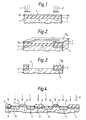
- the semiconductor device body illustrated at an early stage of manufacture in Figure I comprises a main body portion 1 of semiconductor material (for example p type monocrystalline silicon) having an insulating layer 2 (for example of thermally-grown silicon dioxide) at its upper major surface. Ions are implanted into a region 3 (shown in broken outline in Figure 1) by deflecting a narrow focussed ion beam 4 across the upper major surface. In the situation illustrated in Figure 1, at least some of the ions of the beam 4 are of sufficient energy to be implanted in the semiconductor body portion 1 after penetrating the insulating layer 2 and an overlying layer 5.
- semiconductor material for example p type monocrystalline silicon
- insulating layer 2 for example of thermally-grown silicon dioxide
- the pattern of the region 3 into which the ions are implanted is written in the body by controlling the movement of the narrow beam 4 across the upper major surface; when it is desired to form implanted regions which are not connected with each other in the implantation pattern, a shutter may be used or the beam may be widely deflected adjacent its source in known manner to prevent the beam 4 from reaching the device body.
- the beam 4 may consist of ions of a single chemical species or two or more chemical species, depending on the particular ion source used for the beam.
- the beam 4 in Figure 1 is deflected in an annular or grid-like pattern to form an annular or grid-like implanted region 3 in the semiconductor body portion 1.
- the dotted arrows 4' in Figure 1 illustrate the beam 4 after it has been deflected around from the left-hand side of Figure 1 to the right-hand side.
- the implanted ions of the beam 4 may be dopant atoms characteristic of one conductivity type (either n type or p type) in the semiconductor body portion 1 or may be atoms with different characteristics (for example, forming carrier-recombination centres in the semiconductor material).
- the implanted region 3 may be annealed in known manner during or/and after the implantation.
- the implantation into the region 3 is effected through a layer 5 of ion-sensitive resist provided on the upper major surface of the device body. Therefore, at the same time as the implantation occurs into the region 3, the layer 5 is exposed by the ion beam 4 in the area overlying the region 3.
- This ion-exposed area of the layer 5 is designated by the reference 5a in Figure 1 and has a pattern corresponding to that of the region 3.
- the exposure and implantation may be carried out in such conditions that one species of the ions is implanted in the body portion 1 while another species which has a different mass and range is stopped in the resist layer 5 (or possibly the insulating layer 2) depending on its thickness.
- the non-exposed area of the layer 5 is subsequently removed by developing in known manner in a developing solution which dissolves the non-exposed area at least more rapidly than the ion-exposed area 5a.
- the resulting structure having a window in the resist layer 5 is illustrated in Figure 2.
- the remaining ion-exposed area 5a of the resist layer 5 is then used as a mask during a subsequent processing step in the manufacture of the device.
- Figure 3 illustrates the use of the resist area 5a as an etchant mask to localise removal of the insulating layer 2 during an etching step to form a window 6 in the layer 2 at the semiconductor device body surface.
- the layer 2 is removed in this manner from an area not overlying the implanted region 3.
- the resist area 5a may be dissolved away before effecting subsequent processing steps, or it may be retained for a further processing step.
- dopant may be introduced into the body portion I via the window 6 in the insulating layer 2 either after or before the resist area 5a is removed.
- the resist area 5a serves as a mask to define at least partly the lateral extent of this further dopant introduction.
- the dopant introduction is masked solely by the insulating layer 2 the pattern of which has been defined by the resist area 5a.
- the resist area 5a may be adequate to act wholly as the dopant mask or may act as the mask in combination with the underlying layer 2. In some device manufacturing processes, the resist area 5a may even be used as a dopant mask before or instead of its use as an etchant mask.
- the ion beam 4 may comprise boron ions which are implanted to form a more highly doped p type grid pattern 3 in a p type body portion 1.
- the ion-exposed grid-shaped area 5a of the layer 5 is used as an etchant mask to define in a thick (so-called "field") insulating layer 2 a plurality of windows 6 at each of which an insulated-gate field-effect transistor (10 to 12) is formed. Two such windows 6 are illustrated in Figures 4 and 5.
- the resist area 5a may be removed before forming any of the parts 10 to 12 of these transistors.
- a thin insulating layer may be provided at the semiconductor surface exposed in the windows 6, and a stripe 13 of material for forming the gate of the transistor is then provided locally on the thin insulating layer 12 across each window 6 so as to divide the window 6 into two separate areas where the separate source and drain regions 10 and 11 are to be formed.
- Opposite conductivity type determining dopant (for example arsenic) is then introduced into the p type body portion 1 at the windows 6 to form n type source and drain regions 10 and 11 which are located beside the p type grid region 3.
- the lateral extent of these source and drain regions 10 and 11 is defined directly by the window pattern of the insulating layer 2 (and therefore indirectly by the ion-exposed resist area 5a) and by the insulated gate stripe 13.
- This dopant introduction may be effected by flooding the upper major surface of the device body with a wide beam 9 of arsenic ions, as illustrated in Figure 4.
- the parts 10 to 12 of the transistors may be provided in known manner.
- the gate insulating layer 12 may be of silicon dioxide thermally grown at the silicon surface in the windows 6.
- the gate stripe 13 may comprise (either separately or in combination) metal or metal silicide or polycrystalline silicon doped either before or during the formation of the source and drain regions 10 and 11.
- the source and drain regions may be formed by implantation through the areas of the insulating layer 12 not masked by the gate stripe 13 (as illustrated in Figure 4), or these areas of the insulating layer 12 may be removed before forming the source and drain regions by implantation or diffusion.
- a further insulating layer may then be deposited, after which contact windows are opened in the insulating layer structure for contacting the gates 13 and source and drain regions 10 and 11.
- a metallization pattern 15 is then provided to contact the gates 13 and source and drain regions 10 and 11 and to interconnect the transistors in a desired circuit configuration.
- the grid region 3, with which the overlying field insulating layer pattern 2 has been automatically aligned, is sufficiently highly doped to prevent the occurrence of parasitic channels (of the same conductivity type as the source and drain regions 10 and 11) below the parts of the insulating layer 2 between the windows 6 at which the transistors 10 to 13 are located.
- the conductive channel of each transistor is formed in the normal manner below its insulated gate 13 between its source and drain zones 10 and 11.
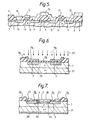
- the ion beam 4 may again comprise boron ions which are implanted to form a highly doped p type annular portion of the transistor base region in an n type body portion 1.
- the body portion 1 may be an n type silicon epitaxial layer 1 on a more highly doped n type substrate 21.
- the resist layer 5 which is exposed by means of the beam 4 during the implantation may be present on an insulating layer 2 which in the form shown in Figure 6 has parts 2a and 2b of different thicknesses and a stepped upper major surface.
- the insulating layer 2 is thinner (part 2b) at an area where the base and emitter regions of the transistor are to be formed.
- the beam 4 is deflected in an annular pattern to form an annular ion-exposed resist area 5a over an annular implanted region 3.
- the inner periphery of the implanted region 3 is defined by the ion beam 4 and so is aligned with the inner periphery of the resist area 5a, whereas the outer periphery of the region 3 is defined by the inner periphery of the thick part 2a of the insulating layer 2; the ion-exposed resist area 5a overlaps this thick part 2a.
- Figure 6 illustrates a processing step after the resist layer 5 has been developed to form the resist mask 5a.
- this step at least the resist area 5a and the thick insulating layer part 2a are used as a mask while introducing both p and n type dopants into the area of the body portion 1 laterally surrounded by the p type region 3 so as to form an active base region 23 and an emitter region 24 of the transistor.
- the area of the thin insulating layer part 2b not covered by the resist area 5a may be removed (by etching using the resist area 5a as an etchant mask) before effecting these dopant introductions.
- the whole upper major surface of the device body is flooded with a wide beam 25 of n type dopant ions (e.g. arsenic) to provide the emitter region 24 at the window in the resist area 5a.
- n type dopant ions e.g. arsenic
- the active base region 23 may be provided in a similar manner using a wide beam of boron ions, either before or after the arsenic implantation.
- the implanted structure may be heated subsequently to anneal the implants and to diffuse slightly the implanted dopants in the body portion 1 to obtain optimum doping profiles for the regions 3, 23 and 24.
- the regions 23 and 24 may be formed entirely by dopant diffusion (without using implantation) into the body portion 1 after removing the area of the thin insulating layer part 2b not covered by the resist area 5a.
- An emitter contact window 6 may be formed by etching away the area of the thin insulating layer part 2b not covered by the resist area 5a while using the resist area 5a as an etchant mask. Base contact windows are also opened by etching away an area of the thin insulating layer part 2b adjacent the thick insulating layer part 2a. Subsequently an emitter and base metallization pattern 26,27 is provided at the upper major surface, and the bottom surface of the substrate 21 may be metallised to form a collector electrode 28. In this device, the region 3 forms a base contact region which laterally surrounds the opposite conductivity type emitter region 24 formed at the window in the resist area 5a.
- the beam 4 is deflected in an annular or grid-like pattern so as to define a non-exposed window area bounded by the ion-exposed resist area 5a and to form an ion-implanted region 3 which laterally surrounds a non-implanted area of the body portion 1.
- the invention may be used to form discrete ion-exposed resist areas 5a which are bounded by grid-like or annular non-exposed areas and below which discrete implanted regions 3 are formed laterally surrounded by grid-like or annular non-implanted areas of the body portion.
- implanted regions 3 may be formed in a layer, for example a silicon layer, at the device body surface instead of in the underlying semiconductor body portion 1.
- a wide variety of different device structures and patterns may be formed for the implanted regions 3 and resist areas 5a.
- the ion-exposed resist areas 5a are used subsequently as etchant and/or dopant masks.
- the resist areas 5a may be used as masks in quite different processing steps.
- a metal layer may be deposited over the resist area 5a and over the remainder of the device body surface not covered by the resist area 5a, after which the resist area 5a may be removed to lift off the part of the metal layer on the area 5a and to leave the remaining part of the metal layer on the device body surface.
- This remaining part of the metal layer may provide an electrode pattern in the semiconductor device and/or it may itself be used as a mask in a subsequent processing step.
- the gates 13 may be formed after the source and drain regions 10 and 11 in the manufacture of the field-effect transistors of Figures 4 and 5.
- a focussed narrow beam comprising arsenic ions may be deflected to form the source and drain regions 10 and 11 by implantation while at the same time exposing an ion-sensitive resist layer on the body surface; the area of the resist overlying the (non-implanted) channel area between the regions 10 and 11 is not exposed by this beam.
- a conductive layer may be deposited over the upper surface including the remaining ion-exposed areas of the resist which are then subsequently removed to lift off the overlying parts of the conductive layer and to leave remaining parts which provide the gates 13.
Landscapes
- Bipolar Transistors (AREA)
- Electron Beam Exposure (AREA)
- Element Separation (AREA)
- Drying Of Semiconductors (AREA)
- Insulated Gate Type Field-Effect Transistor (AREA)
Abstract
Description
- This invention relates to methods of manufacturing a semiconductor device using a beam of ions, particularly but not exclusively for the manufacture of bipolar transistors and insulated-gate field-effect transistors, for example in integrated circuits.
- In the article entitled "Si MOSFET Fabrication Using Focussed Ion Beams" by R. L. Kubena et al I.E.E.E. Transactions on Electron Devices, Vol. ED-31, No. 9, September 1984, pages 1186 to 1189, there is described one specific example of a method of manufacturing a semiconductor device in which ions are implanted into a region of a semiconductor device body by deflecting in a pattern across a major surface of the body a beam of ions which are of sufficient energy to be implanted in the body. In the particular example described, source, drain and channel regions of a p channel depletion mode field-effect transistor (FET) are formed in an n type silicon body by implantation of boron ions from a source of boron and platinum, the platinum ions present in the beam being stopped by a trapping layer of aluminium at the body surface.
- This I.E.E.E. Transactions article also describes the quite separate use of a beam of silicon ions from a gold-silicon liquid-metal-alloy source for ion-beam lithography to expose a layer of ion-sensitive resist in an area where a gate of an n channel enhancement mode field-effect transistor (FET) is to be formed from an underlying molybdenum or polycrystalline silicon layer on a thin silicon dioxide layer at a major surface of the device body. The non-exposed area of the layer of resist is removed by developing, and the exposure pattern is transferred into the underlying molybdenum or polycrystalline silicon layer by plasma or reactive ion etching so as to form a metal-on-oxide-on-semiconductor (MOS) insulated gate of the FET.
- According to the present invention a method of manufacturing a semiconductor device, in which ions are implanted into a region of a semiconductor device body by deflecting in a pattern across a major surface of the body a beam of ions which are of sufficient energy to be implanted in the body, is characterised in that the implantation into said region is effected through a layer of ion-sensitive resist provided on the major surface of the body, which layer is exposed by the ion beam in the area overlying said region of the body at the same time as the implantation occurs into said region, after which the non-exposed area of the layer is removed by developing the resist, and the ion-exposed area of the resist layer is then used as a mask during a subsequent processing step in the manufacture of the device.
- The present invention is based on the recognition that it can be advantageous in semiconductor device manufacture to define a mask pattern of resist using the same processing step as is used to define the same pattern for an implanted region underlying the mask pattern and that this can be achieved in a particularly simple manner using an ion beam to expose an area of ion-sensitive resist at the same time as at least some of said ions are implanted into the desired region through the layer of resist. In this manner the pattern of the underlying implanted region is automatically aligned with and corresponds to the pattern of the mask formed from the ion-sensitive resist.
- It should be noted that the automatic alignment obtained using an ion-beam in this manner in accordance with the invention results directly in the same pattern for the implanted region and for the resist area which is to be used as a mask during a subsequent processing step in the device manufacture. Conventional processes for achieving automatic alignment normally result directly in a pattern which is the inverse (i.e. of complementary shape) to that of a resist area defined not using ion-beam lithography. Specific examples of two such conventional processes are given in United Kingdom patent applications (GB-A) 1355806 and 2024504, in which metal layer patterns are formed with complementary shape to photoresist patterns. In each case additional automatic alignment steps are necessary to obtain an implanted region having the same pattern as a mask which is to be used subsequently in the device manufacture. Thus, in GB-A 1355806 the implanted region is formed with a complementary shape to the metal layer pattern by dopant implantation around the metal layer pattern, and in GB-A 2024504 an implanted region is formed by implantation around the photoresist area so as to have a complementary shape to the photoresist area and therefore the same shape as the metal layer pattern which is to be used subseqently as a mask in the device manufacture. Therefore, compared with these known processes, a significant reduction in the number of processing steps necessary to provide an implanted region and a mask having the same pattern can be achieved in accordance with the present invention.
- The ion-exposed area of the resist layer may be used as a mask for localising various treatments, e.g. etching or/and doping, during subsequent processing steps. The beam may comprise ions of a dopant characteristic of one conductivity type which are implanted to form a region of the one conductivity type, and the ion-exposed area of the resist layer may be used as a mask to define (either directly or indirectly) at least partly the lateral extent of a region of the opposite conductivity type which is formed in a part of the body beside the region of said one conductivity type. Such regions of said one and said opposite conductivity type may be employed in different forms in various devices. Thus, for example, the region of said opposite conductivity type may be a source or drain region of a field-effect transistor, and the implanted region of said one conductivity type may be sufficiently highly doped to prevent the occurrence of a parasitic channel of said opposite conductivity type below an insulating layer around the active regions of the transistor. In another form the device may comprise a bipolar transistor an emitter region of which may be provided by, for example, said region of the opposite conductivity type, and the implanted region of said one conductivity type may form a highly doped portion of a base region which laterally surrounds the emitter region.
- These and other features in accordance with the invention will be illustrated more specifically in embodiments of the invention now to be described, by way of example, with reference to the accompanying diagrammatic drawings, in which:
- Figure 1 is a cross-sectional view of part of a semiconductor device body at one stage in the manufacture of a semiconductor device by a method in accordance with the invention;
- Figure 2 is a partly cross-sectional and partly perspective view of the body part of Figure 1 at a subsequent stage in the manufacture;
- Figure 3 is a cross-sectional view of the body part of Figure 2 at a next stage in the manufacture;
- Figure 4 is a cross-sectional view of part of a semiconductor device body of an integrated circuit at a stage in its manufacture subsequent to the stage illustrated in Figure 3;
- Figure 5 is a cross-sectional view of the body part of Figure 4 showing MOS transistors formed in this integrated circuit;
- Figure 6 is a cross-sectional view of part of a semiconductor device body of an n-p-n bipolar transistor at a stage in its manufacture subsequent to the stage illustrated in Figure 2 or Figure 3, and
- Figure 7 is a cross-sectional view of the body part of Figure 6 after subsequent processing to form the bipolar transistor.
- It should be noted that all of the Figures are diagrammatic and not drawn to scale. The relative dimensions and proportions of parts of these Figures (particularly some of the thicknesses) have been shown exaggerated or diminished for the sake of clarity and convenience in the drawings. The same reference signs as used in one embodiment are generally used when referring to corresponding or similar parts in other embodiments.
- The semiconductor device body illustrated at an early stage of manufacture in Figure I comprises a
main body portion 1 of semiconductor material (for example p type monocrystalline silicon) having an insulating layer 2 (for example of thermally-grown silicon dioxide) at its upper major surface. Ions are implanted into a region 3 (shown in broken outline in Figure 1) by deflecting a narrow focussed ion beam 4 across the upper major surface. In the situation illustrated in Figure 1, at least some of the ions of the beam 4 are of sufficient energy to be implanted in thesemiconductor body portion 1 after penetrating theinsulating layer 2 and anoverlying layer 5. The pattern of theregion 3 into which the ions are implanted is written in the body by controlling the movement of the narrow beam 4 across the upper major surface; when it is desired to form implanted regions which are not connected with each other in the implantation pattern, a shutter may be used or the beam may be widely deflected adjacent its source in known manner to prevent the beam 4 from reaching the device body. The beam 4 may consist of ions of a single chemical species or two or more chemical species, depending on the particular ion source used for the beam. - As will be evident from the subsequent Figures, the beam 4 in Figure 1 is deflected in an annular or grid-like pattern to form an annular or grid-like implanted
region 3 in thesemiconductor body portion 1. The dotted arrows 4' in Figure 1 illustrate the beam 4 after it has been deflected around from the left-hand side of Figure 1 to the right-hand side. Depending on the device to be manufactured, the implanted ions of the beam 4 may be dopant atoms characteristic of one conductivity type (either n type or p type) in thesemiconductor body portion 1 or may be atoms with different characteristics (for example, forming carrier-recombination centres in the semiconductor material). The implantedregion 3 may be annealed in known manner during or/and after the implantation. - In accordance with the present invention the implantation into the
region 3 is effected through alayer 5 of ion-sensitive resist provided on the upper major surface of the device body. Therefore, at the same time as the implantation occurs into theregion 3, thelayer 5 is exposed by the ion beam 4 in the area overlying theregion 3. This ion-exposed area of thelayer 5 is designated by thereference 5a in Figure 1 and has a pattern corresponding to that of theregion 3. When the beam 4 consists of more than one chemical species, the exposure and implantation may be carried out in such conditions that one species of the ions is implanted in thebody portion 1 while another species which has a different mass and range is stopped in the resist layer 5 (or possibly the insulating layer 2) depending on its thickness. The non-exposed area of thelayer 5 is subsequently removed by developing in known manner in a developing solution which dissolves the non-exposed area at least more rapidly than the ion-exposedarea 5a. The resulting structure having a window in theresist layer 5 is illustrated in Figure 2. The remaining ion-exposedarea 5a of theresist layer 5 is then used as a mask during a subsequent processing step in the manufacture of the device. - Figure 3 illustrates the use of the
resist area 5a as an etchant mask to localise removal of theinsulating layer 2 during an etching step to form awindow 6 in thelayer 2 at the semiconductor device body surface. Thelayer 2 is removed in this manner from an area not overlying the implantedregion 3. After this etching step theresist area 5a may be dissolved away before effecting subsequent processing steps, or it may be retained for a further processing step. Thus, for example, dopant may be introduced into the body portion I via thewindow 6 in theinsulating layer 2 either after or before theresist area 5a is removed. In both cases, theresist area 5a serves as a mask to define at least partly the lateral extent of this further dopant introduction. When this further dopant introduction is effected after removing theresist area 5a, the dopant introduction is masked solely by theinsulating layer 2 the pattern of which has been defined by theresist area 5a. When it is effected before removing theresist area 5a, theresist area 5a may be adequate to act wholly as the dopant mask or may act as the mask in combination with theunderlying layer 2. In some device manufacturing processes, theresist area 5a may even be used as a dopant mask before or instead of its use as an etchant mask. - All these various possible combinations of processing steps permit the invention to be used in the manufacture of a wide variety of semiconductor devices and are particularly useful for forming a dopant-implanted
region 3 of one conductivity type in thebody portion 1 and a further region (e.g. 10, 11 or 24) which has the opposite conductivity type in a part of thebody portion 1 beside theregion 3. Two quite different forms will now be illustrated with reference to Figures 4 and 5 (in which said further regions of opposite conductivity type are source anddrain regions emitter region 24 of a bipolar transistor). - In the manufacturing process leading to the fabrication of the MOS integrated circuit of Figure 5, the ion beam 4 may comprise boron ions which are implanted to form a more highly doped p
type grid pattern 3 in a ptype body portion 1. The ion-exposed grid-shaped area 5a of thelayer 5 is used as an etchant mask to define in a thick (so-called "field")insulating layer 2 a plurality ofwindows 6 at each of which an insulated-gate field-effect transistor (10 to 12) is formed. Twosuch windows 6 are illustrated in Figures 4 and 5. Theresist area 5a may be removed before forming any of theparts 10 to 12 of these transistors. - Thus, after removing the
resist area 5a, a thin insulating layer may be provided at the semiconductor surface exposed in thewindows 6, and astripe 13 of material for forming the gate of the transistor is then provided locally on the thin insulatinglayer 12 across eachwindow 6 so as to divide thewindow 6 into two separate areas where the separate source anddrain regions type body portion 1 at thewindows 6 to form n type source and drainregions type grid region 3. The lateral extent of these source and drainregions area 5a) and by theinsulated gate stripe 13. This dopant introduction may be effected by flooding the upper major surface of the device body with awide beam 9 of arsenic ions, as illustrated in Figure 4. - The
parts 10 to 12 of the transistors may be provided in known manner. Thus, for example, thegate insulating layer 12 may be of silicon dioxide thermally grown at the silicon surface in thewindows 6. Thegate stripe 13 may comprise (either separately or in combination) metal or metal silicide or polycrystalline silicon doped either before or during the formation of the source and drainregions layer 12 not masked by the gate stripe 13 (as illustrated in Figure 4), or these areas of the insulatinglayer 12 may be removed before forming the source and drain regions by implantation or diffusion. - A further insulating layer may then be deposited, after which contact windows are opened in the insulating layer structure for contacting the
gates 13 and source and drainregions metallization pattern 15 is then provided to contact thegates 13 and source and drainregions grid region 3, with which the overlying field insulatinglayer pattern 2 has been automatically aligned, is sufficiently highly doped to prevent the occurrence of parasitic channels (of the same conductivity type as the source and drainregions 10 and 11) below the parts of the insulatinglayer 2 between thewindows 6 at which thetransistors 10 to 13 are located. The conductive channel of each transistor is formed in the normal manner below itsinsulated gate 13 between its source and drainzones - In the manufacturing process leading to the fabrication of the n-p-n bipolar transistor of Figure 7, the ion beam 4 may again comprise boron ions which are implanted to form a highly doped p type annular portion of the transistor base region in an n
type body portion 1. In this example thebody portion 1 may be an n typesilicon epitaxial layer 1 on a more highly dopedn type substrate 21. Also in this example, the resistlayer 5 which is exposed by means of the beam 4 during the implantation may be present on an insulatinglayer 2 which in the form shown in Figure 6 hasparts layer 2 is thinner (part 2b) at an area where the base and emitter regions of the transistor are to be formed. The beam 4 is deflected in an annular pattern to form an annular ion-exposed resistarea 5a over an annular implantedregion 3. In this particular example, as illustrated in Figure 6, the inner periphery of the implantedregion 3 is defined by the ion beam 4 and so is aligned with the inner periphery of the resistarea 5a, whereas the outer periphery of theregion 3 is defined by the inner periphery of thethick part 2a of the insulatinglayer 2; the ion-exposed resistarea 5a overlaps thisthick part 2a. - Figure 6 illustrates a processing step after the resist
layer 5 has been developed to form the resistmask 5a. In this step, at least the resistarea 5a and the thick insulatinglayer part 2a are used as a mask while introducing both p and n type dopants into the area of thebody portion 1 laterally surrounded by thep type region 3 so as to form anactive base region 23 and anemitter region 24 of the transistor. If so desired the area of the thin insulatinglayer part 2b not covered by the resistarea 5a may be removed (by etching using the resistarea 5a as an etchant mask) before effecting these dopant introductions. - In Figure 6 the whole upper major surface of the device body is flooded with a
wide beam 25 of n type dopant ions (e.g. arsenic) to provide theemitter region 24 at the window in the resistarea 5a. Theactive base region 23 may be provided in a similar manner using a wide beam of boron ions, either before or after the arsenic implantation. The implanted structure may be heated subsequently to anneal the implants and to diffuse slightly the implanted dopants in thebody portion 1 to obtain optimum doping profiles for theregions regions body portion 1 after removing the area of the thin insulatinglayer part 2b not covered by the resistarea 5a. - An
emitter contact window 6 may be formed by etching away the area of the thin insulatinglayer part 2b not covered by the resistarea 5a while using the resistarea 5a as an etchant mask. Base contact windows are also opened by etching away an area of the thin insulatinglayer part 2b adjacent the thick insulatinglayer part 2a. Subsequently an emitter andbase metallization pattern substrate 21 may be metallised to form acollector electrode 28. In this device, theregion 3 forms a base contact region which laterally surrounds the opposite conductivitytype emitter region 24 formed at the window in the resistarea 5a. - It will be evident that many other modifications are possible within the scope of the invention. In the embodiments illustrated in Figures 1 to 7 the beam 4 is deflected in an annular or grid-like pattern so as to define a non-exposed window area bounded by the ion-exposed resist
area 5a and to form an ion-implantedregion 3 which laterally surrounds a non-implanted area of thebody portion 1. However, the invention may be used to form discrete ion-exposed resistareas 5a which are bounded by grid-like or annular non-exposed areas and below which discrete implantedregions 3 are formed laterally surrounded by grid-like or annular non-implanted areas of the body portion. Furthermore the implantedregions 3 may be formed in a layer, for example a silicon layer, at the device body surface instead of in the underlyingsemiconductor body portion 1. Thus, a wide variety of different device structures and patterns may be formed for the implantedregions 3 and resistareas 5a. - In the embodiments illustrated in Figures 1 to 7, the ion-exposed resist
areas 5a are used subsequently as etchant and/or dopant masks. However, the resistareas 5a may be used as masks in quite different processing steps. Thus, for example, a metal layer may be deposited over the resistarea 5a and over the remainder of the device body surface not covered by the resistarea 5a, after which the resistarea 5a may be removed to lift off the part of the metal layer on thearea 5a and to leave the remaining part of the metal layer on the device body surface. This remaining part of the metal layer may provide an electrode pattern in the semiconductor device and/or it may itself be used as a mask in a subsequent processing step. - In this way, for example, the
gates 13 may be formed after the source and drainregions wide beam 9, a focussed narrow beam, comprising arsenic ions may be deflected to form the source and drainregions regions gates 13.
Claims (6)
Applications Claiming Priority (2)
| Application Number | Priority Date | Filing Date | Title |
|---|---|---|---|
| GB8506489 | 1985-03-13 | ||
| GB08506489A GB2172427A (en) | 1985-03-13 | 1985-03-13 | Semiconductor device manufacture using a deflected ion beam |
Publications (2)
| Publication Number | Publication Date |
|---|---|
| EP0201111A2 true EP0201111A2 (en) | 1986-11-12 |
| EP0201111A3 EP0201111A3 (en) | 1988-08-17 |
Family
ID=10575916
Family Applications (1)
| Application Number | Title | Priority Date | Filing Date |
|---|---|---|---|
| EP86200352A Withdrawn EP0201111A3 (en) | 1985-03-13 | 1986-03-07 | Semiconductor device manufacture using an implantation step |
Country Status (4)
| Country | Link |
|---|---|
| US (1) | US5037767A (en) |
| EP (1) | EP0201111A3 (en) |
| JP (1) | JPS61247023A (en) |
| GB (1) | GB2172427A (en) |
Cited By (1)
| Publication number | Priority date | Publication date | Assignee | Title |
|---|---|---|---|---|
| EP0476801A3 (en) * | 1990-09-20 | 1992-04-01 | Mitsubishi Denki Kabushiki Kaisha | Production of a semiconductor device using implantation into a thermohardening resin |
Families Citing this family (9)
| Publication number | Priority date | Publication date | Assignee | Title |
|---|---|---|---|---|
| US5384268A (en) * | 1993-01-22 | 1995-01-24 | United Microelectronics Corporation | Charge damage free implantation by introduction of a thin conductive layer |
| JP3003542B2 (en) * | 1995-05-24 | 2000-01-31 | 日本電気株式会社 | Method for manufacturing semiconductor device |
| JPH08316168A (en) * | 1995-05-24 | 1996-11-29 | Nec Corp | Method for manufacturing semiconductor device |
| US7238597B2 (en) * | 2002-09-27 | 2007-07-03 | Brontek Delta Corporation | Boron ion delivery system |
| US6767809B2 (en) | 2002-11-19 | 2004-07-27 | Silterra Malayisa Sdn. Bhd. | Method of forming ultra shallow junctions |
| US9580836B2 (en) | 2006-11-22 | 2017-02-28 | Soitec | Equipment for high volume manufacture of group III-V semiconductor materials |
| RU2399115C1 (en) * | 2009-08-13 | 2010-09-10 | Открытое акционерное общество "Восход"-Калужский радиоламповый завод | METHOD FOR ION ALLOYING OF p-n BARRIER AREAS OF SEMICONDUCTOR INSTRUMENTS AND INTEGRATED CIRCUITS WITH BORON |
| US8372737B1 (en) * | 2011-06-28 | 2013-02-12 | Varian Semiconductor Equipment Associates, Inc. | Use of a shadow mask and a soft mask for aligned implants in solar cells |
| FR3003687B1 (en) * | 2013-03-20 | 2015-07-17 | Mpo Energy | METHOD FOR DOPING SILICON PLATES |
Family Cites Families (16)
| Publication number | Priority date | Publication date | Assignee | Title |
|---|---|---|---|---|
| GB1355806A (en) * | 1970-12-09 | 1974-06-05 | Mullard Ltd | Methods of manufacturing a semiconductor device |
| US3950188A (en) * | 1975-05-12 | 1976-04-13 | Trw Inc. | Method of patterning polysilicon |
| US4140547A (en) * | 1976-09-09 | 1979-02-20 | Tokyo Shibaura Electric Co., Ltd. | Method for manufacturing MOSFET devices by ion-implantation |
| GB2024504B (en) * | 1978-06-29 | 1982-10-20 | Philips Electronic Associated | Manufacture of integrated circuits |
| US4347654A (en) * | 1980-06-18 | 1982-09-07 | National Semiconductor Corporation | Method of fabricating a high-frequency bipolar transistor structure utilizing permeation-etching |
| JPS58131A (en) * | 1981-06-24 | 1983-01-05 | Mitsubishi Electric Corp | Etching method for surface protective film |
| US4398964A (en) * | 1981-12-10 | 1983-08-16 | Signetics Corporation | Method of forming ion implants self-aligned with a cut |
| GB2117175A (en) * | 1982-03-17 | 1983-10-05 | Philips Electronic Associated | Semiconductor device and method of manufacture |
| JPS5941870A (en) * | 1982-08-25 | 1984-03-08 | Toshiba Corp | Manufacture of semiconductor device |
| JPS59119728A (en) * | 1982-12-24 | 1984-07-11 | Toshiba Corp | Manufacture of semiconductor device |
| NL8301262A (en) * | 1983-04-11 | 1984-11-01 | Philips Nv | METHOD FOR MANUFACTURING A SEMICONDUCTOR DEVICE APPLYING PATTERNS IN A LOW SILICON NITRIDE USING AN ION IMPLANTATION |
| US4566937A (en) * | 1984-10-10 | 1986-01-28 | The United States Of America As Represented By The United States Department Of Energy | Electron beam enhanced surface modification for making highly resolved structures |
| US4601778A (en) * | 1985-02-25 | 1986-07-22 | Motorola, Inc. | Maskless etching of polysilicon |
| US4748103A (en) * | 1986-03-21 | 1988-05-31 | Advanced Power Technology | Mask-surrogate semiconductor process employing dopant protective region |
| GB2190790B (en) * | 1986-05-12 | 1989-12-13 | Plessey Co Plc | Improvements in transistors |
| JPH0797606B2 (en) * | 1986-10-22 | 1995-10-18 | 株式会社日立製作所 | Method for manufacturing semiconductor integrated circuit device |
-
1985
- 1985-03-13 GB GB08506489A patent/GB2172427A/en not_active Withdrawn
-
1986
- 1986-03-07 EP EP86200352A patent/EP0201111A3/en not_active Withdrawn
- 1986-03-10 JP JP61050696A patent/JPS61247023A/en active Pending
-
1989
- 1989-09-29 US US07/415,398 patent/US5037767A/en not_active Expired - Fee Related
Cited By (4)
| Publication number | Priority date | Publication date | Assignee | Title |
|---|---|---|---|---|
| EP0476801A3 (en) * | 1990-09-20 | 1992-04-01 | Mitsubishi Denki Kabushiki Kaisha | Production of a semiconductor device using implantation into a thermohardening resin |
| US5300445A (en) * | 1990-09-20 | 1994-04-05 | Mitsubishi Denki Kabushiki Kaisha | Production method of an HEMT semiconductor device |
| US5387529A (en) * | 1990-09-20 | 1995-02-07 | Mitsubishi Denki Kabushiki Kaisha | Production method of a MESFET semiconductor device |
| EP0706202A3 (en) * | 1990-09-20 | 1996-05-22 | Mitsubishi Electric Corp |
Also Published As
| Publication number | Publication date |
|---|---|
| US5037767A (en) | 1991-08-06 |
| EP0201111A3 (en) | 1988-08-17 |
| GB2172427A (en) | 1986-09-17 |
| JPS61247023A (en) | 1986-11-04 |
| GB8506489D0 (en) | 1985-04-17 |
Similar Documents
| Publication | Publication Date | Title |
|---|---|---|
| US4394182A (en) | Microelectronic shadow masking process for reducing punchthrough | |
| US4149307A (en) | Process for fabricating insulated-gate field-effect transistors with self-aligned contacts | |
| US4912053A (en) | Ion implanted JFET with self-aligned source and drain | |
| JP3521246B2 (en) | Field effect transistor and method of manufacturing the same | |
| US4798810A (en) | Method for manufacturing a power MOS transistor | |
| CZ62997A3 (en) | Process for producing gated semiconductor device mos with limited number of masks | |
| US4975382A (en) | Method of making a self-aligned field-effect transistor by the use of a dummy-gate | |
| EP0136632A2 (en) | A single mask process for implanting self-aligned source and drain electrodes to form a cmos structure | |
| US4398964A (en) | Method of forming ion implants self-aligned with a cut | |
| US5037767A (en) | Method of manufacturing a semiconductor device by ion implantation through an ion-sensitive resist | |
| US4214359A (en) | MOS Devices having buried terminal zones under local oxide regions | |
| US4114256A (en) | Reliable metal-to-junction contacts in large-scale-integrated devices | |
| US5677213A (en) | Method for forming a semiconductor device having a shallow junction and a low sheet resistance | |
| JPH023269A (en) | Manufacture of integrated circuit | |
| US4675981A (en) | Method of making implanted device regions in a semiconductor using a master mask member | |
| EP0874389B1 (en) | A method of producing MOSFET transistors by means of tilted implants | |
| US6800528B2 (en) | Method of fabricating LDMOS semiconductor devices | |
| JPH09223797A (en) | Method for manufacturing semiconductor device | |
| US20020102785A1 (en) | Method for forming shallow junctions by increasing width of photoresist and using implanting through poly film | |
| US5187117A (en) | Single diffusion process for fabricating semiconductor devices | |
| EP0008774A1 (en) | A method of manufacturing a device in a silicon wafer | |
| CA1138123A (en) | Self-aligned semiconductor method | |
| JP2931243B2 (en) | Method for manufacturing semiconductor device | |
| EP0851478B1 (en) | Method of forming oxide isolation regions | |
| US4685194A (en) | Direct moat self-aligned field oxide technique |
Legal Events
| Date | Code | Title | Description |
|---|---|---|---|
| PUAI | Public reference made under article 153(3) epc to a published international application that has entered the european phase |
Free format text: ORIGINAL CODE: 0009012 |
|
| AK | Designated contracting states |
Kind code of ref document: A2 Designated state(s): DE FR GB NL |
|
| PUAL | Search report despatched |
Free format text: ORIGINAL CODE: 0009013 |
|
| RAP3 | Party data changed (applicant data changed or rights of an application transferred) |
Owner name: N.V. PHILIPS' GLOEILAMPENFABRIEKEN Owner name: PHILIPS ELECTRONIC AND ASSOCIATED INDUSTRIES LIMIT |
|
| AK | Designated contracting states |
Kind code of ref document: A3 Designated state(s): DE FR GB NL |
|
| 17P | Request for examination filed |
Effective date: 19890209 |
|
| 17Q | First examination report despatched |
Effective date: 19910121 |
|
| STAA | Information on the status of an ep patent application or granted ep patent |
Free format text: STATUS: THE APPLICATION IS DEEMED TO BE WITHDRAWN |
|
| RAP3 | Party data changed (applicant data changed or rights of an application transferred) |
Owner name: N.V. PHILIPS' GLOEILAMPENFABRIEKEN Owner name: PHILIPS ELECTRONICS UK LIMITED |
|
| 18D | Application deemed to be withdrawn |
Effective date: 19911029 |
|
| RIN1 | Information on inventor provided before grant (corrected) |
Inventor name: DANIEL, PETER JAMES |