EP0201158B1 - Soudure par vagues vibrantes - Google Patents
Soudure par vagues vibrantes Download PDFInfo
- Publication number
- EP0201158B1 EP0201158B1 EP86301258A EP86301258A EP0201158B1 EP 0201158 B1 EP0201158 B1 EP 0201158B1 EP 86301258 A EP86301258 A EP 86301258A EP 86301258 A EP86301258 A EP 86301258A EP 0201158 B1 EP0201158 B1 EP 0201158B1
- Authority
- EP
- European Patent Office
- Prior art keywords
- solder
- nozzle
- solder wave
- wave
- path
- Prior art date
- Legal status (The legal status is an assumption and is not a legal conclusion. Google has not performed a legal analysis and makes no representation as to the accuracy of the status listed.)
- Expired - Lifetime
Links
Images

Classifications
-
- B—PERFORMING OPERATIONS; TRANSPORTING
- B23—MACHINE TOOLS; METAL-WORKING NOT OTHERWISE PROVIDED FOR
- B23K—SOLDERING OR UNSOLDERING; WELDING; CLADDING OR PLATING BY SOLDERING OR WELDING; CUTTING BY APPLYING HEAT LOCALLY, e.g. FLAME CUTTING; WORKING BY LASER BEAM
- B23K3/00—Tools, devices or special appurtenances for soldering, e.g. brazing, or unsoldering, not specially adapted for particular methods
- B23K3/06—Solder feeding devices; Solder melting pans
- B23K3/0646—Solder baths
- B23K3/0653—Solder baths with wave generating means, e.g. nozzles, jets, fountains
-
- B—PERFORMING OPERATIONS; TRANSPORTING
- B23—MACHINE TOOLS; METAL-WORKING NOT OTHERWISE PROVIDED FOR
- B23K—SOLDERING OR UNSOLDERING; WELDING; CLADDING OR PLATING BY SOLDERING OR WELDING; CUTTING BY APPLYING HEAT LOCALLY, e.g. FLAME CUTTING; WORKING BY LASER BEAM
- B23K3/00—Tools, devices or special appurtenances for soldering, e.g. brazing, or unsoldering, not specially adapted for particular methods
- B23K3/06—Solder feeding devices; Solder melting pans
- B23K3/0646—Solder baths
- B23K3/0661—Oscillating baths
-
- B—PERFORMING OPERATIONS; TRANSPORTING
- B23—MACHINE TOOLS; METAL-WORKING NOT OTHERWISE PROVIDED FOR
- B23K—SOLDERING OR UNSOLDERING; WELDING; CLADDING OR PLATING BY SOLDERING OR WELDING; CUTTING BY APPLYING HEAT LOCALLY, e.g. FLAME CUTTING; WORKING BY LASER BEAM
- B23K2101/00—Articles made by soldering, welding or cutting
- B23K2101/36—Electric or electronic devices
- B23K2101/42—Printed circuits
-
- H—ELECTRICITY
- H05—ELECTRIC TECHNIQUES NOT OTHERWISE PROVIDED FOR
- H05K—PRINTED CIRCUITS; CASINGS OR CONSTRUCTIONAL DETAILS OF ELECTRIC APPARATUS; MANUFACTURE OF ASSEMBLAGES OF ELECTRICAL COMPONENTS
- H05K3/00—Apparatus or processes for manufacturing printed circuits
- H05K3/30—Assembling printed circuits with electric components, e.g. with resistors
- H05K3/32—Assembling printed circuits with electric components, e.g. with resistors electrically connecting electric components or wires to printed circuits
- H05K3/34—Assembling printed circuits with electric components, e.g. with resistors electrically connecting electric components or wires to printed circuits by soldering
- H05K3/3465—Application of solder
- H05K3/3468—Application of molten solder, e.g. dip soldering
Definitions
- the present invention relates to wave soldering of printed wiring boards. More specifically, the preset invention relates to wave soldering of surface mounted devices or components on printed wiring boards as well as standard components on single sided, double sided and/or multi-layer boards.
- the present methods of wave soldering surface mounted devices on printed wiring boards include systems having two solder waves.
- the first solder wave typically has a narrow turbulent parabolic shape.
- the narrow wave contacts a small area on the wiring board allowing gases to escape.
- the gases are generated by flux volatiles and the like, which can inhibit solder wetting.
- the narrow wave also provides a vertical pressure to force solder into the small spaces and openings between the components to ensure that all circuit pads, components, terminations, contacts, and the like, are wetted with solder.
- the second solder wave is typically a solder wave as used in commercially available machines for soldering printed wiring boards with leaded components and the like.
- the second wave completes the process and provides optimum exit conditions for the printed wiring boards leaving the solder wave to minimize or eliminate excess solder deposits and eliminate bridges between contacts.
- the dual solder wave process has proven to be effective for soldering surface mounted devices onto printed wiring boards, but the process suffers from certain disadvantages.
- One problem is excessive dross (oxide) production. Dual wave systems typically produce up to twice as much dross as single wave systems.
- Another problem is the lack of fine control of a turbulent parabolic solder wave. Best soldering results have been obtained by immersing the printed wiring board as deeply as possible in this wave. However, the turbulence of the wave makes this task difficult and may result in solder flooding onto the top side of the printed wiring boards.
- a still further problem with the dual solder wave process can occur when particles of dross, particles of carbonized oil or other particles in the solder stream block or partially block the narrow nozzle of the first solder wave. Such a blockage can affect the turbulent flow.
- the present invention consists in a process for wave soldering a prefluxed element such as wave soldering surface mounted devices to a prefluxed printed wiring board, comprising the steps of moving the element along a predetermined path, forming a solder wave having a predetermined configuration beneath the path, so that at least a portion of the element passes through the solder wave, and producing an oscillation in the solder wave during the passage of the element therethrough, characterised in that the oscillation has a frequency in the range from 20 to 400 Hz.
- the invention also consists in apparatus for wave soldering a prefluxed element such as surface mounted devices to a prefluxed printed wiring board, comprising means for moving the element along a predetermined path so that at least a portion of the element passes through a solder wave of predetermined configuration formed beneath the path, and oscillating means for producing oscillations in the solder wave during the passage of the element therethrough, characterised in that the oscillating means comprises at least one vibrating vane disposed in the solder wave, and a vibrator for oscillating the vibrating vane at a frequency in the range from 20 to 400 Hz.
- the oscillation or vibration provided in the solder wave aids in filling small holes in a board, crevices, corners adjacent to solder masks and all other areas where solder wetting is difficult to achieve with conventional machines.
- An additional benefit is overcoming problems that occur with thick dry film solder mask.
- a relatively high frequency oscillation in the solder wave displaces or dislodges gas bubbles that form beneath the boards, allowing the solder to reach all areas in the matrix of components on the printed wiring boards, overcoming the repelling effect of any non-metallized elements such as component bodies, solder masks and the like.
- the vibrating or oscillating concept of the present invention can be applied to existing types of solder wave machines for wave soldering, either as a permanent installation or a temporary installation for soldering certain difficult to solder elements.
- the frequency of the oscillation and/ or the amplitude of the oscillation are controlled and at least one vibrating zone is formed in the solder wave.
- the oscillation occurs in a direction substantially parallel to the path of the element and, in another embodiment, the oscillation occurs in a direction substantially perpendicular to the path of the element.
- the vibrating vane may be in the form of a flat strip and extends in the solder wave substantially perpendicular to the path of the wiring board, and the vibrator oscillates the flat strip in a direction substantially parallel to the path of the wiring board.
- a plurality of vibrating vanes are joined by a connector rod, and the vibrator oscillates the vanes in a direction substantially perpendicular to the path of the wiring board.
- Means is preferably provided to enable adjustment of the frequency and/or amplitude of vibration over the frequency range of 20 to 400 cycles per second, and an amplitude range up to at least about 1.5 mm (0.060 ins.). Furthermore, the position of the vane in the solder wave is preferably adjustable. Means is also provided in one embodiment for optionally feeding a surface additive, such as oil, to the solder wave.
- a surface additive such as oil
- the solder wave is formed from a discharge nozzle facing upwards positioned above a solder reservoir with a pump means for forming the solder wave from the nozzle.
- a vibrating vane is, in one embodiment, positioned in the solder wave and at least two zones of vibration are formed.
- At least one adjustable passive vane is located in the solder wave downstream from the discharge nozzle at the element exit side.
- the position of the passive vane provides a further zone of vibration to aid in separation of the element, such as a wiring board or the like, from the solder wave.
- At least one liquid surface additive feeding tube may be positioned downstream of the passive vane and means is provided to supply liquid surface additive through the feeding tube to the surface of the solder wave.
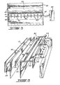
- Fig. 1 and 2 illustrate cross sections through a typical solder wave nozzle 10 such as that shown in Canadian Patent 1,002,391 to Elliott et al.
- the nozzle 10 is connected to a solder supply conduit 11 by means of a flange 12. Solder enters the nozzle 10 and forms the desired shape of solder wave. The solder flows back into a solder pot 13.S;v, are
- solder pot 13 Above the solder pot 13 is a wiring board, path 14 along which wiring boards 15 are conveyed.
- the drawings illustrate a straight inclined path 14, however, the present invention may be applied to solder wave machines with horizontal or curved paths. Furthermore, the elements to be soldered may follow dip type paths in the solder wave as a reciprocal dip, curved dip or other path. Such a dipping step may be used for tinning one or more surfaces.
- the printed wiring boards 15 have - surface mounted devices 16 with pads and contacts 17 to be coated with solder and form soldered connectios.
- the entry side of the nozzle 10 has a guide 20 to provide a downward sloping path for a portion of the solder..
- the exit solder wave flows to a weir plate 21.
- Fig. 1 shows a vibrating vane 30 in the form of a flat strip positioned in the nozzle-10 extending along the length of the nozzle.
- the vane 30 has a top edge shown to be substantially the same height as the top edge of the nozzle 10.
- the top edge of the vane 30 may be below the top edge of the nozzle or higher than the top edge of the nozzle provided it is not so high as to- interfere with passage of the assembly being soldered.
- a connecting rod 31 which in some nozzles may be two or more rods, pass through an aperture 32; in the exit side of the nozzle 10 to supports the vane 30.
- the rods 31 connect to as vibrator 33 positioned away from the solder nozzle 10 above the solder pot 13.
- the exact position of the vibrator 33 as well as the rods 31 to the vane or vanes 30 may be varied.
- the vibrator may be located above or below the solder wave and is supported to ensure that vibration isitransmitted to the vane 30.
- the frequency and/or amplitude of vibration is controllable by the vibrator 33.
- solder wave It is preferred to vibrate the solder wave a sufficient amount so that gas bubbles that form beneath the wiring board 15 are displaced or dislodged, allowing solder to reach component terminations and other hard to reach areas to be soldered: Large gas bubbles may be broken into smaller ones and all the bubbles are continuously shifted allowing the solder to reach all areas.
- the vibration is also sufficient to cause the molten solder to be forced up on either side of the surface mounted devices overcoming the repelling effect of the non metallized component bodies.
- the solder then wets the metallic areas to be soldered; such: as component terminations, pads etcetera or forms solder joints as required.
- the vibrating frequency together with the amplitude of vibration is adjustable to suit different types of wiring boards.
- Figs 2 and 3 illustrate another embodiment wherein a series of short individual vanes 40 are positioned perpendicular to the length of the nozzle 10 and have a connecting rod 41 connecting all the vanes 40 together. Wherein one rod 41 is shown, it would be apparent that two or more rods may be used if necessary.
- the rod 41 is supported at apertures 42 in the end plates 43 of the nozzle 10 and is connected to a vibrator 44 such that vibration occurs in a different plane to that shown in Fig. 1.
- Fig. 1 illustrates that vibrations or oscillations occur substantially parallel with the travel of the wiring board path 14, and
- Figs. 2 and 3 show that vibrations or oscillations occur substantially perpendicular to the travel of the wiring board path 14.
- the position of the vanes 40 in the nozzle 10 may be raised or lowered and the number of vanes 40 may depend on the particular type of wave soldering machine and the particular type of printed wiring boards being soldered.
- the size, shape, quantity and angle of vanes can be varied as required.
- the vibrations or oscillations may be applied at any angle between the two directions shown in Figs. 1 and 2.
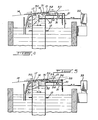
- the vibrating vane 30 is connected to the vibrator 33 by one or more connecting rods 31.As shown in this figure, the top edge of the vibrating vane 30 protrudes slightly above the top edge of the nozzle 10. The top edge of the vane 30 must not interfere with the surface mounted devices on the wiring board 15.
- the position ofthe vibrating vane 30 is adjustable for optimizing the vibrating characteristics and soldering results.
- the wiring board path in Fig. 4 has a slope of 6o upwards in the direction oftravel. The slope angle of the path may vary from about 0 to 10° dependent upon the type of solder machine. Furthermore, curved paths or dip type paths may be provided through the solder wave.
- two solderwave vibrating zones 50 and 51 are shown, one on each side of the vibrating vane 30 under the wiring board 15. These zones 50 and 51 allow the solder to reach all the areas requiring solder wetting.
- A.further zone or zones of vibration 52 is formed by using a passive vane 53 on the exit side of the nozzle 10 before the weir plate 21.
- the passive vane 53 may be located at the most suitable position avoiding the components on the printed wiring board 15, and the further vibration zone 52 preferably occurs between the nozzle and the weir. In one embodiment the further vibration zone occurs at the point or close to the point of separation of the board 15 from the solder wave.
- the passive vane 53 also has a damping effect on the solder located between the weir 21 and the passive vane 53.
- the U-shaped passive vane 53 shown in the drawing may be located at different positions in the exit trough 54 to vary the position of the further zone 52.
- FIGs. 5 and 6 show a modification to the apparatus shown in Fig. 4 wherein a feeding tube 55 for a surface additive such as oil, is positioned adjacent to the weir 21 which allows an oil reservoir 56 to be formed between the tube 55 and the surface of the solder.
- a thin coating of oil or other surface additive is created on the surface of the solder wave that reduces surface tension and at the same time reduces dross formation on the wave surface.
- vanes need not necessarily be located in the nozzle itself, but may be positioned in the solder stream between the nozzle exit and the weir 21.
- the vanes may be positioned on the input side of the solder wave indicated as zone 50 in Figs. 4 and 5. There are no random parameters in the vibratory wave because the frequency of oscillation and amplitude of oscillation are precisely controlled.
- the shape or form of the vanes may be varied in orderto applyvibration at a suitable location in the solder wave. The suitable location being one which displaces or dislodges gas bubbles from underneath the wiring board, and allows solder to reach all areas to be soldered.
- the vibrator can produce a frequency in the range of 20 to 400 cycles per second and can also vary the amplitude of vibration up to at least about 1.5 mm (0.060 inches).
Landscapes
- Engineering & Computer Science (AREA)
- Mechanical Engineering (AREA)
- Electric Connection Of Electric Components To Printed Circuits (AREA)
- Molten Solder (AREA)
Claims (26)
Priority Applications (1)
| Application Number | Priority Date | Filing Date | Title |
|---|---|---|---|
| MYPI87001369A MY100436A (en) | 1985-05-03 | 1987-08-18 | Vibratory wave soldering. |
Applications Claiming Priority (4)
| Application Number | Priority Date | Filing Date | Title |
|---|---|---|---|
| GB858511280A GB8511280D0 (en) | 1985-05-03 | 1985-05-03 | Vibratory wave soldering |
| GB8511280 | 1985-05-03 | ||
| CA000494984A CA1230426A (fr) | 1985-05-03 | 1985-11-08 | Soudure a la vague a vibrations pour cartes a cablage imprime |
| CA494984 | 1985-11-08 |
Publications (3)
| Publication Number | Publication Date |
|---|---|
| EP0201158A2 EP0201158A2 (fr) | 1986-11-12 |
| EP0201158A3 EP0201158A3 (en) | 1987-06-03 |
| EP0201158B1 true EP0201158B1 (fr) | 1990-12-12 |
Family
ID=25670832
Family Applications (1)
| Application Number | Title | Priority Date | Filing Date |
|---|---|---|---|
| EP86301258A Expired - Lifetime EP0201158B1 (fr) | 1985-05-03 | 1986-02-21 | Soudure par vagues vibrantes |
Country Status (9)
| Country | Link |
|---|---|
| US (1) | US4684056A (fr) |
| EP (1) | EP0201158B1 (fr) |
| CN (1) | CN1003975B (fr) |
| AU (1) | AU580236B2 (fr) |
| BR (1) | BR8601972A (fr) |
| DE (1) | DE3676111D1 (fr) |
| MY (1) | MY100436A (fr) |
| NZ (1) | NZ215973A (fr) |
| SG (1) | SG36191G (fr) |
Families Citing this family (26)
| Publication number | Priority date | Publication date | Assignee | Title |
|---|---|---|---|---|
| DE3765359D1 (de) * | 1986-08-13 | 1990-11-08 | Senju Metal Industry Co | Loetgeraet des springbrunnentyps. |
| KR920008948B1 (ko) * | 1987-02-12 | 1992-10-12 | 니혼 덴네쯔 게이기 가부시끼가이샤 | 프린트 기판의 납땜방법 및 그의 장치 |
| NL8701237A (nl) * | 1987-05-22 | 1988-12-16 | Soltec Bv | Inrichting voor het aanbrengen van geleidend hechtmiddel, zoals soldeer, op een kaart met bedrukte bedrading. |
| US4821947A (en) * | 1988-02-08 | 1989-04-18 | Union Carbide Corporation | Fluxless application of a metal-comprising coating |
| US4802617A (en) * | 1988-02-19 | 1989-02-07 | Electrovert Limited | Restriction of dross formation in a soldering apparatus |
| IT1216594B (it) * | 1988-04-19 | 1990-03-08 | Italtel Spa | Metodo e dispositivo per la saldatura ad onda. |
| US4886201A (en) * | 1988-06-09 | 1989-12-12 | Electrovert Limited | Solder wave nozzle construction |
| US5044542A (en) * | 1989-11-22 | 1991-09-03 | Electrovert Ltd. | Shield gas wave soldering |
| US5121874A (en) * | 1989-11-22 | 1992-06-16 | Electrovert Ltd. | Shield gas wave soldering |
| US5048746A (en) * | 1989-12-08 | 1991-09-17 | Electrovert Ltd. | Tunnel for fluxless soldering |
| GB9001361D0 (en) * | 1990-01-20 | 1990-03-21 | Blundell Production Equipment | Soldering apparatus |
| US5090651A (en) * | 1990-01-31 | 1992-02-25 | Electrovert Ltd. | Gas curtain additives and zoned tunnel for soldering |
| US5228614A (en) * | 1990-07-09 | 1993-07-20 | Electrovert Ltd. | Solder nozzle with gas knife jet |
| JPH04172174A (ja) * | 1990-10-31 | 1992-06-19 | Yokota Kikai Kk | 自動半田付け方法及び装置 |
| GB9123549D0 (en) * | 1991-11-06 | 1992-01-02 | Automation Limited | Chip waves |
| US5148961A (en) * | 1991-12-23 | 1992-09-22 | Motorola, Inc. | Selective wave solder apparatus |
| US5295214A (en) * | 1992-11-16 | 1994-03-15 | International Business Machines Corporation | Optical module with tolerant wave soldered joints |
| US5409155A (en) * | 1993-04-23 | 1995-04-25 | Solectron Croporation | Vibrational self aligning parts in a solder reflow process |
| US5690766A (en) * | 1995-08-16 | 1997-11-25 | The Trustees Of The University Of Pennsylvania | Method and apparatus for decreasing the time needed to die bond microelectronic chips |
| JPH11151572A (ja) * | 1997-11-17 | 1999-06-08 | Tamagawa Seiki Co Ltd | ハンダ付け方法及び装置 |
| GB2371006B (en) * | 2001-01-10 | 2005-05-04 | Evenoak Ltd | Nozzle for soldering apparatus |
| US7918383B2 (en) * | 2004-09-01 | 2011-04-05 | Micron Technology, Inc. | Methods for placing substrates in contact with molten solder |
| DE102014110720B4 (de) * | 2014-07-29 | 2025-12-31 | Illinois Tool Works Inc. | Lötmodul |
| US9370838B2 (en) | 2014-08-21 | 2016-06-21 | Illinois Tool Works Inc. | Wave soldering nozzle system and method of wave soldering |
| CN104588814B (zh) * | 2014-11-18 | 2016-08-31 | 北京三重华星电子科技有限公司 | 一种波峰焊夹具制作规范的方法 |
| JP2019171400A (ja) * | 2018-03-27 | 2019-10-10 | 株式会社デンソーテン | はんだ減勢装置 |
Family Cites Families (13)
| Publication number | Priority date | Publication date | Assignee | Title |
|---|---|---|---|---|
| CA718666A (en) * | 1965-09-28 | Electrovert Manufacturing Co. Ltd. | Molten solder bath with uniformly dispersed additive | |
| FR1217793A (fr) * | 1958-12-09 | 1960-05-05 | Perfectionnements à la fabrication des éléments semi-conducteurs | |
| US3266136A (en) * | 1963-03-29 | 1966-08-16 | Western Electric Co | Mass soldering apparatus and method using vibratory energy |
| US3303983A (en) * | 1964-11-12 | 1967-02-14 | Gen Dynamics Corp | Ultrasonic soldering apparatus |
| US3430332A (en) * | 1966-04-01 | 1969-03-04 | Electrovert Mfg Co Ltd | Production line soldering with application of ultrasonic energy directing to molten solder |
| US3605244A (en) * | 1966-04-20 | 1971-09-20 | Electrovert Mfg Co Ltd | Soldering methods and apparatus |
| US3536243A (en) * | 1968-01-08 | 1970-10-27 | Branson Instr | Ultrasonic soldering apparatus |
| US3989180A (en) * | 1971-11-10 | 1976-11-02 | Electrovert Manufacturing Company, Limited | Wave soldering with supported inclined wave |
| CA1002391A (en) * | 1974-10-07 | 1976-12-28 | Electrovert Ltd. - Electrovert Ltee | Wave-soldering of printed circuits |
| US3990621A (en) * | 1976-01-07 | 1976-11-09 | Hollis Engineering, Inc. | Static head soldering system with oil |
| JPS6051939B2 (ja) * | 1981-06-02 | 1985-11-16 | 権士 近藤 | 噴流式はんだ槽 |
| GB2117690B (en) * | 1982-04-02 | 1986-01-08 | Zevatron Gmbh | Apparatus for soldering workpieces |
| DE3240540A1 (de) * | 1982-11-03 | 1984-06-14 | GeWerTec Gesellschaft für Werkstofftechnik mbH, 4600 Dortmund | Verfahren und vorrichtung zum hochtemperatur- und hartloeten |
-
1986
- 1986-02-19 US US06/830,962 patent/US4684056A/en not_active Ceased
- 1986-02-21 EP EP86301258A patent/EP0201158B1/fr not_active Expired - Lifetime
- 1986-02-21 DE DE8686301258T patent/DE3676111D1/de not_active Expired - Lifetime
- 1986-04-24 AU AU56745/86A patent/AU580236B2/en not_active Ceased
- 1986-04-28 NZ NZ215973A patent/NZ215973A/xx unknown
- 1986-05-02 CN CN86103013.3A patent/CN1003975B/zh not_active Expired
- 1986-05-02 BR BR8601972A patent/BR8601972A/pt not_active IP Right Cessation
-
1987
- 1987-08-18 MY MYPI87001369A patent/MY100436A/en unknown
-
1991
- 1991-05-13 SG SG361/91A patent/SG36191G/en unknown
Also Published As
| Publication number | Publication date |
|---|---|
| EP0201158A3 (en) | 1987-06-03 |
| DE3676111D1 (de) | 1991-01-24 |
| NZ215973A (en) | 1988-10-28 |
| CN86103013A (zh) | 1986-10-29 |
| AU580236B2 (en) | 1989-01-05 |
| CN1003975B (zh) | 1989-04-19 |
| SG36191G (en) | 1991-06-21 |
| AU5674586A (en) | 1986-11-06 |
| EP0201158A2 (fr) | 1986-11-12 |
| MY100436A (en) | 1990-09-29 |
| BR8601972A (pt) | 1987-01-06 |
| US4684056A (en) | 1987-08-04 |
Similar Documents
| Publication | Publication Date | Title |
|---|---|---|
| US4684056A (en) | Vibratory wave soldering | |
| US5156324A (en) | Solder apparatus with dual hollow wave nozzles | |
| EP0083680B1 (fr) | Soudage à onde de circuits intégrés | |
| JP4253374B2 (ja) | プリント基板のはんだ付け方法および噴流はんだ槽 | |
| EP0688254B1 (fr) | Buse de brasage avec un couteau a jet de gaz | |
| CA2016716C (fr) | Appareil de soudage a vague, sous gaz protecteur | |
| EP0278166B1 (fr) | Appareil de soudage | |
| US4402448A (en) | Mass soldering system | |
| USRE33197E (en) | Vibrator wave soldering | |
| US4401253A (en) | Mass soldering system | |
| WO1992010323A1 (fr) | Brasage tendre a la vague a gaz de protection | |
| EP0147001A1 (fr) | Système II à souder par ondes destiné à la fabrication en masse | |
| US4540114A (en) | Apparatus for soldering workpieces | |
| KR20010088301A (ko) | 프린트 기판의 납땜방법 및 자동 납땜장치 | |
| CA1230426A (fr) | Soudure a la vague a vibrations pour cartes a cablage imprime | |
| JPS63268563A (ja) | 印刷配線回路板をはんだでマス結合する装置 | |
| JP2005177845A (ja) | 噴流式はんだ付け装置 | |
| JPH0790360B2 (ja) | 回路基板へのハンダ付け方法及びその装置 | |
| JPS6315063B2 (fr) | ||
| JP2803663B2 (ja) | 自動半田付け装置のノズル構造 | |
| JPS59178169A (ja) | 半田付装置 | |
| SU819992A1 (ru) | Устройство дл удалени излишковпРипО из ОТВЕРСТий и C пОВЕРХНОСТипЕчАТНыХ плАТ | |
| GB2173136A (en) | Soldering surface mounted devices to flat surfaces | |
| CA2155351C (fr) | Buse de machine a braser a jet de gaz coupant | |
| JPH0783174B2 (ja) | プリント基板のはんだ付け方法およびその装置 |
Legal Events
| Date | Code | Title | Description |
|---|---|---|---|
| PUAI | Public reference made under article 153(3) epc to a published international application that has entered the european phase |
Free format text: ORIGINAL CODE: 0009012 |
|
| AK | Designated contracting states |
Kind code of ref document: A2 Designated state(s): CH DE FR GB IT LI NL SE |
|
| PUAL | Search report despatched |
Free format text: ORIGINAL CODE: 0009013 |
|
| AK | Designated contracting states |
Kind code of ref document: A3 Designated state(s): CH DE FR GB IT LI NL SE |
|
| 17P | Request for examination filed |
Effective date: 19871127 |
|
| 17Q | First examination report despatched |
Effective date: 19881219 |
|
| GRAA | (expected) grant |
Free format text: ORIGINAL CODE: 0009210 |
|
| AK | Designated contracting states |
Kind code of ref document: B1 Designated state(s): CH DE FR GB IT LI NL SE |
|
| ITF | It: translation for a ep patent filed | ||
| REF | Corresponds to: |
Ref document number: 3676111 Country of ref document: DE Date of ref document: 19910124 |
|
| ET | Fr: translation filed | ||
| ITTA | It: last paid annual fee | ||
| PLBI | Opposition filed |
Free format text: ORIGINAL CODE: 0009260 |
|
| 26 | Opposition filed |
Opponent name: ITALTEL SOCIETA' ITALIANA TELECOMUNICAZIONI S.P.A. Effective date: 19910906 |
|
| NLR1 | Nl: opposition has been filed with the epo |
Opponent name: ITALTEL SOCIETA' ITALIANA TELECOMUNICAZIONI S.P.A. |
|
| PLBN | Opposition rejected |
Free format text: ORIGINAL CODE: 0009273 |
|
| STAA | Information on the status of an ep patent application or granted ep patent |
Free format text: STATUS: OPPOSITION REJECTED |
|
| 27O | Opposition rejected |
Effective date: 19930508 |
|
| NLR2 | Nl: decision of opposition | ||
| EAL | Se: european patent in force in sweden |
Ref document number: 86301258.9 |
|
| REG | Reference to a national code |
Ref country code: GB Ref legal event code: IF02 |
|
| PGFP | Annual fee paid to national office [announced via postgrant information from national office to epo] |
Ref country code: SE Payment date: 20030226 Year of fee payment: 18 |
|
| PGFP | Annual fee paid to national office [announced via postgrant information from national office to epo] |
Ref country code: CH Payment date: 20040216 Year of fee payment: 19 |
|
| PG25 | Lapsed in a contracting state [announced via postgrant information from national office to epo] |
Ref country code: SE Free format text: LAPSE BECAUSE OF NON-PAYMENT OF DUE FEES Effective date: 20040222 |
|
| PGFP | Annual fee paid to national office [announced via postgrant information from national office to epo] |
Ref country code: NL Payment date: 20040530 Year of fee payment: 20 |
|
| EUG | Se: european patent has lapsed | ||
| PGFP | Annual fee paid to national office [announced via postgrant information from national office to epo] |
Ref country code: DE Payment date: 20050208 Year of fee payment: 20 |
|
| PGFP | Annual fee paid to national office [announced via postgrant information from national office to epo] |
Ref country code: FR Payment date: 20050210 Year of fee payment: 20 |
|
| PGFP | Annual fee paid to national office [announced via postgrant information from national office to epo] |
Ref country code: GB Payment date: 20050214 Year of fee payment: 20 |
|
| PGFP | Annual fee paid to national office [announced via postgrant information from national office to epo] |
Ref country code: IT Payment date: 20050217 Year of fee payment: 20 |
|
| PG25 | Lapsed in a contracting state [announced via postgrant information from national office to epo] |
Ref country code: LI Free format text: LAPSE BECAUSE OF NON-PAYMENT OF DUE FEES Effective date: 20050228 Ref country code: CH Free format text: LAPSE BECAUSE OF NON-PAYMENT OF DUE FEES Effective date: 20050228 |
|
| REG | Reference to a national code |
Ref country code: GB Ref legal event code: PE20 |
|
| REG | Reference to a national code |
Ref country code: CH Ref legal event code: PL |
|
| PG25 | Lapsed in a contracting state [announced via postgrant information from national office to epo] |
Ref country code: GB Free format text: LAPSE BECAUSE OF EXPIRATION OF PROTECTION Effective date: 20060220 |
|
| PG25 | Lapsed in a contracting state [announced via postgrant information from national office to epo] |
Ref country code: NL Free format text: LAPSE BECAUSE OF EXPIRATION OF PROTECTION Effective date: 20060221 |
|
| NLV7 | Nl: ceased due to reaching the maximum lifetime of a patent |
Effective date: 20060221 |