EP0201700A1 - Commande pour enclencher et déclencher des composants semi-conducteurs de puissance - Google Patents
Commande pour enclencher et déclencher des composants semi-conducteurs de puissance Download PDFInfo
- Publication number
- EP0201700A1 EP0201700A1 EP86104210A EP86104210A EP0201700A1 EP 0201700 A1 EP0201700 A1 EP 0201700A1 EP 86104210 A EP86104210 A EP 86104210A EP 86104210 A EP86104210 A EP 86104210A EP 0201700 A1 EP0201700 A1 EP 0201700A1
- Authority
- EP
- European Patent Office
- Prior art keywords
- pulse
- pulse train
- control
- modulation
- thyristor
- Prior art date
- Legal status (The legal status is an assumption and is not a legal conclusion. Google has not performed a legal analysis and makes no representation as to the accuracy of the status listed.)
- Granted
Links
Images
Classifications
-
- H—ELECTRICITY
- H02—GENERATION; CONVERSION OR DISTRIBUTION OF ELECTRIC POWER
- H02M—APPARATUS FOR CONVERSION BETWEEN AC AND AC, BETWEEN AC AND DC, OR BETWEEN DC AND DC, AND FOR USE WITH MAINS OR SIMILAR POWER SUPPLY SYSTEMS; CONVERSION OF DC OR AC INPUT POWER INTO SURGE OUTPUT POWER; CONTROL OR REGULATION THEREOF
- H02M1/00—Details of apparatus for conversion
- H02M1/06—Circuits specially adapted for rendering non-conductive gas discharge tubes or equivalent semiconductor devices, e.g. thyratrons, thyristors
-
- H—ELECTRICITY
- H03—ELECTRONIC CIRCUITRY
- H03K—PULSE TECHNIQUE
- H03K17/00—Electronic switching or gating, i.e. not by contact-making and –breaking
- H03K17/51—Electronic switching or gating, i.e. not by contact-making and –breaking characterised by the components used
- H03K17/56—Electronic switching or gating, i.e. not by contact-making and –breaking characterised by the components used by the use, as active elements, of semiconductor devices
- H03K17/60—Electronic switching or gating, i.e. not by contact-making and –breaking characterised by the components used by the use, as active elements, of semiconductor devices the devices being bipolar transistors
- H03K17/601—Electronic switching or gating, i.e. not by contact-making and –breaking characterised by the components used by the use, as active elements, of semiconductor devices the devices being bipolar transistors using transformer coupling
Definitions
- the invention relates to a method for controlling power semiconductor components that can be switched on and off, the control power being transmitted by means of a pulse train with a transformer and then the pulse train being rectified, and a device for carrying out the method for a switchable thyristor with a transformer, the primary winding of which is via a first controllable switch can be acted upon by a pulse sequence and the two secondary windings are connected to rectifiers, a secondary winding feeding auxiliary voltage parts which can be switched to the gate-cathode path of the thyristor via a second controllable switch.
- the control of power semiconductor components used in power electronics devices generally requires electrical isolation to isolate the control section from the power section.
- conventional thyristors as power semiconductor components, the potential is separated by means of a pulse transformer, which feeds the control currents directly into the gate-cathode section, the control section of the thyristor.
- Pulse-shaped control currents of both polarities are generally required, e.g. a positive pulse for switching on and a negative pulse for switching off the power semiconductor component.
- the control currents or voltages are present, e.g. a positive control current during the switch-on time and a negative control voltage during the switch-off time.
- one of the secondary windings is connected directly to the gate-cathode path of the GTO thyristor via rectifiers.
- the positive control current is fed in via this secondary winding during the switch-on time.
- a capacitor is charged as an auxiliary voltage source, which can be discharged via a transistor onto the primary winding of a second transformer, the secondary winding of which is also connected to the gate-cathode path of the thyristor for feeding in the negative breaking current via diodes.
- several pulse transformers are required, which increases the effort.
- the current steepness of the control currents is limited by the leakage inductances of the pulse transformers. This leads to difficulties, in particular when high demands are placed on the insulation voltage and when controlling high-performance semiconductor components.
- a control part for the electrically isolated control of power transistors is commercially available, in which the control information, i.e. the command for switching the power transistor on or off, is transmitted optoelectronically isolated.
- the control information is used to control a pulse amplifier which alternately connects two auxiliary voltage sources with opposite polarities to the base-emitter path of the power transistor.
- the auxiliary voltage sources which also supply the energy for the pulse amplifier, are also electrically isolated from the control. This circuit is also very complex.
- the object is to design a method of the type mentioned at the outset in such a way that the effort for the potential-separate transmission of both the tax output and the tax information is reduced.
- this object is achieved in that the control information of the pulse train is impressed by modulation and in that the pulse train is demodulated after the electrically isolated transmission.
- both the control power and the control information are transmitted with the same pulse sequence. Therefore, only one insulation gap between the control and power section is required.
- the required pulse transformer can also be designed for high insulation voltage and small volume, since a large leakage inductance is permissible.
- Pulse duration modulation has proven to be particularly advantageous since it can be used to implement a simple demodulator with a low-pass filter with a subsequent comparator.
- the failure of the pulse train can be more certain Switching status can be assigned. If, for example, the smaller pulse-pause ratio is assigned to the switch-off state, the connected semiconductor switch can be switched off automatically if the pulse train fails.
- the first switch can be controlled by a modulation stage and the other secondary winding also feeds an auxiliary voltage source which can be connected to the gate-cathode path of the thyristor via a third controllable switch and a secondary winding is connected to a demodulation stage , whose output signal alternately actuates the second or third switch.
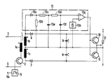
- the figure shows the circuit diagram of a control part, which is operated according to the inventive method.
- the primary winding 1 a of a pulse transformer 1 is connected via a transistor 2 to the terminals 3 and 4 of a DC voltage source.
- the base of transistor 2 is controlled by a modulation stage 5, at the control input 5a of which control pulses are applied.
- An RC oscillator for example, can be used as the modulation stage, which generates a pulse-duration-modulated pulse sequence with a pulse frequency of approximately 1 MHz.
- the trailing edges of the individual pulses are modulated in such a way that a short pulse pause is assigned to state one of the ignition signals, which corresponds to the "thyristor on” command, and a larger pulse pause is assigned to state zero, which corresponds to the "thyristor off” command.
- the two secondary windings 1 and 1 of the pulse transformer 1 are each connected via a diode 6 and 7 to capacitors 8 and 9, which serve as auxiliary voltage sources.
- the capacitors 8 and 9 are applied to the gate-cathode path of the thyristor 12, the cathode of the thyristor 12 being connected to the connection point of the two secondary windings 1b and 1c, which has the potential zero.
- the taps of the secondary winding 1 are also routed to a demodulation stage 13, which in the exemplary embodiment is implemented with a low-pass filter and a comparator connected downstream.
- One tap of the secondary winding 1b is a diode. 13a connected as a rectifier and a bridging resistor 13b.
- the diode 13a is connected to the low-pass filter, to which the resistors 13c and 13d and the capacitors 13e and 13f are connected.
- the output of the low pass is at the non-inverting input of an operational amplifier 13g, the inverting input of which is connected to a threshold voltage source 13h.
- the output of operational amplifier 13g is at the control inputs of transistors 10 and 11, which form the pulse amplifier.
- the pulse duration modulated pulse train transmitted by the transformer 1 is rectified by the rectifiers 6 and 7 and charges the capacitors 8 and 9.
- the pulse train thus serves to transmit the control power.
- the control information impressed with the pulse duration modulation is recovered in the demodulation stage.
- the threshold voltage is selected such that it lies between the maximum value of the output voltage of the low-pass filter, which corresponds to the command "thyristor on", and the minimum value of the output voltage, which is assigned to the command "thyrister off".
- a signal is thus present at the output of the comparator 13g, which is positive for switching on the thyristor 12 and negative for switching off the thyristor 12. With this control signal, the transistors 10 and 11 are driven alternately and the GTO thyristor 12 is ignited or extinguished.
Landscapes
- Engineering & Computer Science (AREA)
- Power Engineering (AREA)
- Power Conversion In General (AREA)
- Electronic Switches (AREA)
- Thyristor Switches And Gates (AREA)
Priority Applications (1)
| Application Number | Priority Date | Filing Date | Title |
|---|---|---|---|
| AT86104210T ATE50383T1 (de) | 1985-04-12 | 1986-03-26 | Ansteuerung fuer ein- und ausschaltbare leistungshalbleiterelemente. |
Applications Claiming Priority (2)
| Application Number | Priority Date | Filing Date | Title |
|---|---|---|---|
| DE19853513170 DE3513170A1 (de) | 1985-04-12 | 1985-04-12 | Verfahren zum ansteuern ein- und ausschaltbarer leistungshalbleiterbauelemente und vorrichtung zur durchfuehrung des verfahrens |
| DE3513170 | 1985-04-12 |
Publications (2)
| Publication Number | Publication Date |
|---|---|
| EP0201700A1 true EP0201700A1 (fr) | 1986-11-20 |
| EP0201700B1 EP0201700B1 (fr) | 1990-02-07 |
Family
ID=6267857
Family Applications (1)
| Application Number | Title | Priority Date | Filing Date |
|---|---|---|---|
| EP86104210A Expired - Lifetime EP0201700B1 (fr) | 1985-04-12 | 1986-03-26 | Commande pour enclencher et déclencher des composants semi-conducteurs de puissance |
Country Status (6)
| Country | Link |
|---|---|
| US (1) | US4767948A (fr) |
| EP (1) | EP0201700B1 (fr) |
| JP (1) | JPS61238121A (fr) |
| AT (1) | ATE50383T1 (fr) |
| CA (1) | CA1285321C (fr) |
| DE (2) | DE3513170A1 (fr) |
Cited By (3)
| Publication number | Priority date | Publication date | Assignee | Title |
|---|---|---|---|---|
| WO1994019700A1 (fr) * | 1993-02-24 | 1994-09-01 | Siemens Aktiengesellschaft | Dispositif permettant de detecter la valeur reelle d'une grandeur mesuree a haut potentiel |
| DE4425901A1 (de) * | 1994-07-21 | 1996-01-25 | Siemens Ag | Regelverstärker zur Steuerung einer hochohmigen Niedersapnnungsquelle |
| DE10218455A1 (de) * | 2002-04-25 | 2003-11-06 | Abb Patent Gmbh | Sperrwandleranordnung |
Families Citing this family (5)
| Publication number | Priority date | Publication date | Assignee | Title |
|---|---|---|---|---|
| US4859921A (en) * | 1988-03-10 | 1989-08-22 | General Electric Company | Electronic control circuits, electronically commutated motor systems, switching regulator power supplies, and methods |
| DE69334054T2 (de) * | 1992-06-15 | 2006-12-07 | Fujitsu Ltd., Kawasaki | Integrierte Halbleiterschaltung mit Eingangs/Ausgangschnittstelle geeignet für niedrige Amplituden |
| DE19534888A1 (de) * | 1995-09-20 | 1997-03-27 | Bosch Gmbh Robert | Schaltungsanordnung zur Mehrfachausnutzung eines Übertragerkerns |
| JP4059330B2 (ja) * | 1998-06-11 | 2008-03-12 | 有限会社 エルメック | Gtoサイリスタのゲートドライブ装置 |
| US20080265936A1 (en) * | 2007-04-27 | 2008-10-30 | Dsm Solutions, Inc. | Integrated circuit switching device, structure and method of manufacture |
Citations (1)
| Publication number | Priority date | Publication date | Assignee | Title |
|---|---|---|---|---|
| DE2913974A1 (de) * | 1979-04-05 | 1980-10-23 | Licentia Gmbh | Steuerschaltung fuer gto-thyristoren |
Family Cites Families (8)
| Publication number | Priority date | Publication date | Assignee | Title |
|---|---|---|---|---|
| US3852620A (en) * | 1972-07-31 | 1974-12-03 | Westinghouse Electric Corp | Electrical pulse generating circuit and method |
| DE2808000C2 (de) * | 1978-02-23 | 1985-01-31 | Licentia Patent-Verwaltungs-Gmbh, 6000 Frankfurt | Verfahren und Anordnung zur Ansteuerung von Leistungshalbleitern |
| JPS607467B2 (ja) * | 1978-06-30 | 1985-02-25 | 松下電器産業株式会社 | 周波数変換装置 |
| DE2852943C3 (de) * | 1978-12-07 | 1981-09-10 | Licentia Patent-Verwaltungs-Gmbh, 6000 Frankfurt | Anordnung mit einem verzögerungsbehafteten Halbleiterschalter |
| JPS57126270A (en) * | 1981-01-29 | 1982-08-05 | Toshiba Corp | Gate controlling circuit for gate turn-off thyristor |
| JPS607570U (ja) * | 1983-06-24 | 1985-01-19 | 昭和アルミニウム株式会社 | 太陽熱集熱装置における管継手 |
| DE3472867D1 (en) * | 1984-02-29 | 1988-08-25 | Ibm | Power switching circuit |
| US4597038A (en) * | 1984-07-26 | 1986-06-24 | Westinghouse Electric Corp. | Switching overlap protection by control gate impedance monitoring |
-
1985
- 1985-04-12 DE DE19853513170 patent/DE3513170A1/de not_active Ceased
-
1986
- 1986-03-18 US US06/840,696 patent/US4767948A/en not_active Expired - Fee Related
- 1986-03-26 DE DE8686104210T patent/DE3669025D1/de not_active Expired - Lifetime
- 1986-03-26 AT AT86104210T patent/ATE50383T1/de active
- 1986-03-26 EP EP86104210A patent/EP0201700B1/fr not_active Expired - Lifetime
- 1986-04-08 JP JP61080958A patent/JPS61238121A/ja active Pending
- 1986-04-10 CA CA000506346A patent/CA1285321C/fr not_active Expired - Lifetime
Patent Citations (1)
| Publication number | Priority date | Publication date | Assignee | Title |
|---|---|---|---|---|
| DE2913974A1 (de) * | 1979-04-05 | 1980-10-23 | Licentia Gmbh | Steuerschaltung fuer gto-thyristoren |
Cited By (3)
| Publication number | Priority date | Publication date | Assignee | Title |
|---|---|---|---|---|
| WO1994019700A1 (fr) * | 1993-02-24 | 1994-09-01 | Siemens Aktiengesellschaft | Dispositif permettant de detecter la valeur reelle d'une grandeur mesuree a haut potentiel |
| DE4425901A1 (de) * | 1994-07-21 | 1996-01-25 | Siemens Ag | Regelverstärker zur Steuerung einer hochohmigen Niedersapnnungsquelle |
| DE10218455A1 (de) * | 2002-04-25 | 2003-11-06 | Abb Patent Gmbh | Sperrwandleranordnung |
Also Published As
| Publication number | Publication date |
|---|---|
| JPS61238121A (ja) | 1986-10-23 |
| DE3669025D1 (de) | 1990-03-15 |
| EP0201700B1 (fr) | 1990-02-07 |
| US4767948A (en) | 1988-08-30 |
| CA1285321C (fr) | 1991-06-25 |
| DE3513170A1 (de) | 1986-10-16 |
| ATE50383T1 (de) | 1990-02-15 |
Similar Documents
| Publication | Publication Date | Title |
|---|---|---|
| DE2654461C2 (de) | Funkenzündungssystem | |
| DE2613423C3 (de) | Elektronisches Schaltgerät | |
| EP0019813B1 (fr) | Commutateur électronique marche-arrêt à effleurement | |
| DE3618221C1 (de) | Schaltnetzteil mit einem primaer getakteten Gleichspannungswandler | |
| DE3424052A1 (de) | Signalumformer | |
| EP0201700B1 (fr) | Commande pour enclencher et déclencher des composants semi-conducteurs de puissance | |
| DE3813672A1 (de) | Wechselrichter fuer eine induktive last | |
| DE2753888C2 (fr) | ||
| DE2554825C3 (de) | Schaltungsanordnung zur Erzeugung einer Ausgangsspannung aus einer von einer Gleichspannungsquelle gelieferten Eingangsgleichspannung abhängig von einer vorgegebenen Sollspannung | |
| DE2555260C3 (de) | Treiberschaltung zur Umsetzung der Übergänge eines nichtsymmetrischen Datencode in eine Folge abwechselnd positiver und negativer, je einen Übergang anzeigender Impulse | |
| EP0171470B1 (fr) | Dispositif d'alimentation d'émetteurs et de récepteurs d'un système de transmission de signaux | |
| AT390532B (de) | Pulsbreiten moduliertes wechselstrom-leistungsstellglied | |
| DE1114537B (de) | Anordnung zur Erhoehung der Schaltgeschwindigkeit eines aus zwei parallelgeschalteten Transistoren bestehenden Kippschalters | |
| DE2427402A1 (de) | Stromversorgungsanordnung | |
| DE2439241C2 (de) | Schaltungsanordnung mit einer ersten periodisch leitenden Schalteinrichtung zur Herstellung eines Übertragungsweges | |
| DE68922178T2 (de) | Datenkommunikationssystem. | |
| DE2621471C3 (de) | Schaltung zur Regelung der Ausgangsspannungen einer Kommutatorablenkschaltung | |
| DE3341767A1 (de) | Spannungsschaltregler | |
| DE3021930A1 (de) | Netzgeraet | |
| EP0489194A1 (fr) | Agencement de circuit | |
| DE2633956A1 (de) | Getaktetes netzgeraet, insbesondere zur abgabe mehrerer stabilisierter gleichspannungen | |
| DE3218357A1 (de) | Vorrichtung zur erzeugung einer geregelten ausgangsspannung | |
| DE3500627A1 (de) | Gleichstrom-gleichstromwandler | |
| DE3109750A1 (de) | Schaltungsanordnung fuer einen wechselrichter zur speisung eines wechselstromverbrauchers mit einer alternierenden spannung, insbesondere einer sinusfoermigen wechselspannung | |
| DE3617374A1 (de) | Gleichspannungswandler mit resonanzkreis |
Legal Events
| Date | Code | Title | Description |
|---|---|---|---|
| PUAI | Public reference made under article 153(3) epc to a published international application that has entered the european phase |
Free format text: ORIGINAL CODE: 0009012 |
|
| AK | Designated contracting states |
Kind code of ref document: A1 Designated state(s): AT CH DE GB LI |
|
| 17P | Request for examination filed |
Effective date: 19861218 |
|
| 17Q | First examination report despatched |
Effective date: 19881124 |
|
| GRAA | (expected) grant |
Free format text: ORIGINAL CODE: 0009210 |
|
| AK | Designated contracting states |
Kind code of ref document: B1 Designated state(s): AT CH DE GB LI |
|
| REF | Corresponds to: |
Ref document number: 50383 Country of ref document: AT Date of ref document: 19900215 Kind code of ref document: T |
|
| REF | Corresponds to: |
Ref document number: 3669025 Country of ref document: DE Date of ref document: 19900315 |
|
| GBT | Gb: translation of ep patent filed (gb section 77(6)(a)/1977) | ||
| PLBE | No opposition filed within time limit |
Free format text: ORIGINAL CODE: 0009261 |
|
| STAA | Information on the status of an ep patent application or granted ep patent |
Free format text: STATUS: NO OPPOSITION FILED WITHIN TIME LIMIT |
|
| 26N | No opposition filed | ||
| PGFP | Annual fee paid to national office [announced via postgrant information from national office to epo] |
Ref country code: CH Payment date: 19940617 Year of fee payment: 9 |
|
| PG25 | Lapsed in a contracting state [announced via postgrant information from national office to epo] |
Ref country code: LI Effective date: 19950331 Ref country code: CH Effective date: 19950331 |
|
| REG | Reference to a national code |
Ref country code: CH Ref legal event code: PL |
|
| PGFP | Annual fee paid to national office [announced via postgrant information from national office to epo] |
Ref country code: DE Payment date: 19960520 Year of fee payment: 11 |
|
| PGFP | Annual fee paid to national office [announced via postgrant information from national office to epo] |
Ref country code: GB Payment date: 19970224 Year of fee payment: 12 |
|
| PGFP | Annual fee paid to national office [announced via postgrant information from national office to epo] |
Ref country code: AT Payment date: 19970305 Year of fee payment: 12 |
|
| PG25 | Lapsed in a contracting state [announced via postgrant information from national office to epo] |
Ref country code: DE Effective date: 19971202 |
|
| PG25 | Lapsed in a contracting state [announced via postgrant information from national office to epo] |
Ref country code: GB Free format text: LAPSE BECAUSE OF NON-PAYMENT OF DUE FEES Effective date: 19980326 Ref country code: AT Free format text: LAPSE BECAUSE OF NON-PAYMENT OF DUE FEES Effective date: 19980326 |
|
| GBPC | Gb: european patent ceased through non-payment of renewal fee |
Effective date: 19980326 |