EP0201954B1 - Halbleiteranordnung mit einer Wärmesenke - Google Patents
Halbleiteranordnung mit einer Wärmesenke Download PDFInfo
- Publication number
- EP0201954B1 EP0201954B1 EP86200648A EP86200648A EP0201954B1 EP 0201954 B1 EP0201954 B1 EP 0201954B1 EP 86200648 A EP86200648 A EP 86200648A EP 86200648 A EP86200648 A EP 86200648A EP 0201954 B1 EP0201954 B1 EP 0201954B1
- Authority
- EP
- European Patent Office
- Prior art keywords
- layer
- support
- copper
- semiconductor device
- cobalt
- Prior art date
- Legal status (The legal status is an assumption and is not a legal conclusion. Google has not performed a legal analysis and makes no representation as to the accuracy of the status listed.)
- Expired - Lifetime
Links
Images
Classifications
-
- H—ELECTRICITY
- H10—SEMICONDUCTOR DEVICES; ELECTRIC SOLID-STATE DEVICES NOT OTHERWISE PROVIDED FOR
- H10W—GENERIC PACKAGES, INTERCONNECTIONS, CONNECTORS OR OTHER CONSTRUCTIONAL DETAILS OF DEVICES COVERED BY CLASS H10
- H10W70/00—Package substrates; Interposers; Redistribution layers [RDL]
- H10W70/20—Conductive package substrates serving as an interconnection, e.g. metal plates
- H10W70/24—Conductive package substrates serving as an interconnection, e.g. metal plates characterised by materials
-
- H—ELECTRICITY
- H10—SEMICONDUCTOR DEVICES; ELECTRIC SOLID-STATE DEVICES NOT OTHERWISE PROVIDED FOR
- H10W—GENERIC PACKAGES, INTERCONNECTIONS, CONNECTORS OR OTHER CONSTRUCTIONAL DETAILS OF DEVICES COVERED BY CLASS H10
- H10W40/00—Arrangements for thermal protection or thermal control
- H10W40/20—Arrangements for cooling
- H10W40/25—Arrangements for cooling characterised by their materials
- H10W40/255—Arrangements for cooling characterised by their materials having a laminate or multilayered structure, e.g. direct bond copper [DBC] ceramic substrates
-
- H—ELECTRICITY
- H10—SEMICONDUCTOR DEVICES; ELECTRIC SOLID-STATE DEVICES NOT OTHERWISE PROVIDED FOR
- H10W—GENERIC PACKAGES, INTERCONNECTIONS, CONNECTORS OR OTHER CONSTRUCTIONAL DETAILS OF DEVICES COVERED BY CLASS H10
- H10W72/00—Interconnections or connectors in packages
- H10W72/30—Die-attach connectors
Definitions
- the invention relates to a semiconductor device comprising a semiconductor element which is secured by means of indium solder on a heat-dissipating support of copper or a copper alloy, a barrier layer being formed between the support and the indium solder.
- Indium solder has the advantage that the melting temperature is comparatively low. It is used, for example, for soldering semiconductor laser elements.
- the semiconductor laser elements are not allowed to reach a high temperature; the support, which has to ensure a good heat dissipation, is chosen to be made mostly of copper.
- indium diffused into copper so that a barrier layer has to be formed between the support and the solder.
- a barrier layer of molybdenum Indium solder has the advantage that the melting temperature is comparatively low. It is used, for example, for soldering semiconductor laser elements.
- the semiconductor laser elements are not allowed to reach a high temperature; the support, which has to ensure a good heat dissipation, is chosen to be made mostly of copper.
- indium diffused into copper so that a barrier layer has to be formed between the support and the solder.
- a barrier layer of molybdenum molybdenum cannot readily be provided and the cost price of molybdenum is high.
- Platinum is also suggested to be used as
- a semiconductor device comprising a semiconductor element which is secured by means of solder on a heat dissipating support of copper or a copper alloy, a barrier layer being provided between the support and the solder, said barrier layer consisting of a cobalt layer coated with a gold layer, the cobalt layer having a thickness between 0.2 and 2 pm and the gold layer having a thickness lying between 1 to 2 um.
- the invention has for its object to provide a semiconductor device of the kind mentioned in the opening paragraph, which has a barrier layer which acts effectively, can be provided in a simple manner and is inexpensive. It is a surprise to find that a very effective barrier between indium and a support of copper or a copper alloy is obtained if the barrier layer consists of a cobalt layer coated with a very thin gold layer. The cobalt layer prevents the diffusion of indium into the copper of the support, while the thin gold layer ensures a good wetting during soldering.
- the cobalt layer has a thickness of at least 2 ⁇ m and the gold layer has a thickness lying beween 0.05pm and 0.1 um.
- the cobalt layer and the gold layer are applied by electrodeposition.
- the fact that the cobalt can be applied by electrodeposition means a considerable simplification in the manufacture with respect to other barrier materials, such as molybdenum.
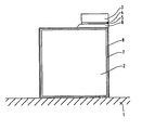
- the Figure shows diagrammatically a support with a semiconductor element secured on it, while for the sake of clarity the parts of the Figure are not all drawn to scale.
- a support 2 for a semiconductor element 3 is secured on a part 1 of an envelope (not shown) of the semiconductor device.
- the semiconductor element 3 may be, for example, a semiconductor laser element, which can be composed in known manner of a plurality of layers of gallium arsenide, and gallium aluminium arsenide.
- the major surface to be soldered of such an element is provided, for example, with a molybdenum layer 4, to which a gold layer 5 is applied.
- the support is made of copper or of a copper alloy. A good dissipation of the heat developed in the laser element 3 is then ensured.
- the semiconductor laser element is secured to the support by indium solder 6.
- the use of the indium has the advantage that the melting temperature during soldering may be comparatively low, i.e. of the order of 160°C to 200°C, depending upon the composition. However, indium solder tends to diffuse into copper. In order to avoid the soldering layer disappearing entirely in the copper, a barrier layer has to be provided.
- a cobalt layer 7 is applied to the support 2 and a very thin gold layer 8 is applied to the cobalt layer 7.
- the gold layer 8 ensures a good wetting during soldering.
- the layers 7 and 8 can be advantageously applied by electrodeposition; they can be present over the whole surface of the support. It is already sufficient when the layers 7 and 8 are present only at the area of the indium solder. However the process of applying the layers thus becomes more complicated. It will be appreciated that the layers 7 and 8 may also be deposited in a different manner, for example by vapour deposition. However, this process is generally more laborious than electrodeposition. It is recommendable, at any rate if the barrier layer is applied only locally to the support, to first apply to the support a thin layer of nickel or nickel phosphorus in order to prevent oxidation of the copper.
Landscapes
- Cooling Or The Like Of Semiconductors Or Solid State Devices (AREA)
- Die Bonding (AREA)
- Semiconductor Lasers (AREA)
- Electroplating Methods And Accessories (AREA)
Claims (2)
Applications Claiming Priority (2)
| Application Number | Priority Date | Filing Date | Title |
|---|---|---|---|
| NL8501153A NL8501153A (nl) | 1985-04-22 | 1985-04-22 | Halfgeleiderinrichting. |
| NL8501153 | 1985-04-22 |
Publications (2)
| Publication Number | Publication Date |
|---|---|
| EP0201954A1 EP0201954A1 (de) | 1986-11-20 |
| EP0201954B1 true EP0201954B1 (de) | 1990-06-27 |
Family
ID=19845868
Family Applications (1)
| Application Number | Title | Priority Date | Filing Date |
|---|---|---|---|
| EP86200648A Expired - Lifetime EP0201954B1 (de) | 1985-04-22 | 1986-04-16 | Halbleiteranordnung mit einer Wärmesenke |
Country Status (5)
| Country | Link |
|---|---|
| EP (1) | EP0201954B1 (de) |
| JP (1) | JPS61248434A (de) |
| KR (1) | KR860008606A (de) |
| DE (1) | DE3672331D1 (de) |
| NL (1) | NL8501153A (de) |
Families Citing this family (3)
| Publication number | Priority date | Publication date | Assignee | Title |
|---|---|---|---|---|
| GB8807729D0 (en) * | 1988-03-31 | 1988-05-05 | British Telecomm | Device mounting |
| US6504242B1 (en) * | 2001-11-15 | 2003-01-07 | Intel Corporation | Electronic assembly having a wetting layer on a thermally conductive heat spreader |
| US20160276242A1 (en) * | 2015-03-20 | 2016-09-22 | Raytheon Company | Thermal spreader having inter-metal diffusion barrier layer |
Family Cites Families (4)
| Publication number | Priority date | Publication date | Assignee | Title |
|---|---|---|---|---|
| GB1331980A (en) * | 1970-12-15 | 1973-09-26 | Mullard Ltd | Mounting semiconductor bodies |
| JPS51140565A (en) * | 1975-05-30 | 1976-12-03 | Nec Home Electronics Ltd | Semiconductor unit |
| JPS6013078B2 (ja) * | 1978-09-05 | 1985-04-04 | 日本特殊陶業株式会社 | 金メツキされた電子部品及びその製法 |
| US4424527A (en) * | 1981-07-31 | 1984-01-03 | Optical Information Systems, Inc. | Bonding pad metallization for semiconductor devices |
-
1985
- 1985-04-22 NL NL8501153A patent/NL8501153A/nl not_active Application Discontinuation
-
1986
- 1986-04-16 DE DE8686200648T patent/DE3672331D1/de not_active Expired - Lifetime
- 1986-04-16 EP EP86200648A patent/EP0201954B1/de not_active Expired - Lifetime
- 1986-04-19 KR KR1019860003038A patent/KR860008606A/ko not_active Withdrawn
- 1986-04-19 JP JP61089230A patent/JPS61248434A/ja active Pending
Also Published As
| Publication number | Publication date |
|---|---|
| NL8501153A (nl) | 1986-11-17 |
| KR860008606A (ko) | 1986-11-17 |
| EP0201954A1 (de) | 1986-11-20 |
| JPS61248434A (ja) | 1986-11-05 |
| DE3672331D1 (de) | 1990-08-02 |
Similar Documents
| Publication | Publication Date | Title |
|---|---|---|
| US4321617A (en) | System for soldering a semiconductor laser to a metal base | |
| US2971251A (en) | Semi-conductive device | |
| DE69231790T2 (de) | Wärmeabführendes Bauteil und damit versehene Halbleitervorrichtung | |
| GB2291886A (en) | Alloy bonding material | |
| US6147403A (en) | Semiconductor body with metallizing on the back side | |
| US4702941A (en) | Gold metallization process | |
| JPH0249021B2 (de) | ||
| US5105258A (en) | Metal system for semiconductor die attach | |
| US3409809A (en) | Semiconductor or write tri-layered metal contact | |
| US5016083A (en) | Submount for semiconductor laser device | |
| US3622385A (en) | Method of providing flip-chip devices with solderable connections | |
| US3567506A (en) | Method for providing a planar transistor with heat-dissipating top base and emitter contacts | |
| EP0201954B1 (de) | Halbleiteranordnung mit einer Wärmesenke | |
| GB2035690A (en) | Semiconductor device and a method of contacting a partial region of a semiconductor surface | |
| US4187599A (en) | Semiconductor device having a tin metallization system and package containing same | |
| US3950142A (en) | Lead assembly for semiconductive device | |
| DE19543245A1 (de) | Halbleitervorrichtung mit flammgespritzter Wärmeausbreitungsschicht und Verfahren für deren Herstellung | |
| GB2300375A (en) | Bonding method for electric element | |
| JPS62122157A (ja) | 光半導体用ヒ−トシンクの電極構造 | |
| CA1153128A (en) | Electrical circuit assemblies | |
| US4921158A (en) | Brazing material | |
| EP0086520B1 (de) | Verfahren zur Metallplattierung | |
| JPS5842243A (ja) | 半導体素子用支持電極板 | |
| JP2001284501A (ja) | 放熱基板 | |
| JPH0420269B2 (de) |
Legal Events
| Date | Code | Title | Description |
|---|---|---|---|
| PUAI | Public reference made under article 153(3) epc to a published international application that has entered the european phase |
Free format text: ORIGINAL CODE: 0009012 |
|
| AK | Designated contracting states |
Kind code of ref document: A1 Designated state(s): DE FR GB IT NL |
|
| 17P | Request for examination filed |
Effective date: 19870508 |
|
| 17Q | First examination report despatched |
Effective date: 19881103 |
|
| GRAA | (expected) grant |
Free format text: ORIGINAL CODE: 0009210 |
|
| AK | Designated contracting states |
Kind code of ref document: B1 Designated state(s): DE FR GB IT NL |
|
| REF | Corresponds to: |
Ref document number: 3672331 Country of ref document: DE Date of ref document: 19900802 |
|
| ITF | It: translation for a ep patent filed | ||
| ET | Fr: translation filed | ||
| PG25 | Lapsed in a contracting state [announced via postgrant information from national office to epo] |
Ref country code: GB Effective date: 19910416 |
|
| PLBE | No opposition filed within time limit |
Free format text: ORIGINAL CODE: 0009261 |
|
| STAA | Information on the status of an ep patent application or granted ep patent |
Free format text: STATUS: NO OPPOSITION FILED WITHIN TIME LIMIT |
|
| 26N | No opposition filed | ||
| PG25 | Lapsed in a contracting state [announced via postgrant information from national office to epo] |
Ref country code: NL Effective date: 19911101 |
|
| GBPC | Gb: european patent ceased through non-payment of renewal fee | ||
| NLV4 | Nl: lapsed or anulled due to non-payment of the annual fee | ||
| PG25 | Lapsed in a contracting state [announced via postgrant information from national office to epo] |
Ref country code: FR Effective date: 19911230 |
|
| PG25 | Lapsed in a contracting state [announced via postgrant information from national office to epo] |
Ref country code: DE Effective date: 19920201 |
|
| REG | Reference to a national code |
Ref country code: FR Ref legal event code: ST |
|
| PG25 | Lapsed in a contracting state [announced via postgrant information from national office to epo] |
Ref country code: IT Free format text: LAPSE BECAUSE OF NON-PAYMENT OF DUE FEES;WARNING: LAPSES OF ITALIAN PATENTS WITH EFFECTIVE DATE BEFORE 2007 MAY HAVE OCCURRED AT ANY TIME BEFORE 2007. THE CORRECT EFFECTIVE DATE MAY BE DIFFERENT FROM THE ONE RECORDED. Effective date: 20050416 |