EP0202573A2 - Cellule de base réalisée en technologie CMOS et procédé pour la configuration automatique d'une telle cellule - Google Patents
Cellule de base réalisée en technologie CMOS et procédé pour la configuration automatique d'une telle cellule Download PDFInfo
- Publication number
- EP0202573A2 EP0202573A2 EP86106433A EP86106433A EP0202573A2 EP 0202573 A2 EP0202573 A2 EP 0202573A2 EP 86106433 A EP86106433 A EP 86106433A EP 86106433 A EP86106433 A EP 86106433A EP 0202573 A2 EP0202573 A2 EP 0202573A2
- Authority
- EP
- European Patent Office
- Prior art keywords
- transistors
- conductor tracks
- cell
- basic cell
- tracks
- Prior art date
- Legal status (The legal status is an assumption and is not a legal conclusion. Google has not performed a legal analysis and makes no representation as to the accuracy of the status listed.)
- Ceased
Links
Images


Classifications
-
- H—ELECTRICITY
- H10—SEMICONDUCTOR DEVICES; ELECTRIC SOLID-STATE DEVICES NOT OTHERWISE PROVIDED FOR
- H10W—GENERIC PACKAGES, INTERCONNECTIONS, CONNECTORS OR OTHER CONSTRUCTIONAL DETAILS OF DEVICES COVERED BY CLASS H10
- H10W20/00—Interconnections in chips, wafers or substrates
- H10W20/40—Interconnections external to wafers or substrates, e.g. back-end-of-line [BEOL] metallisations or vias connecting to gate electrodes
- H10W20/41—Interconnections external to wafers or substrates, e.g. back-end-of-line [BEOL] metallisations or vias connecting to gate electrodes characterised by their conductive parts
- H10W20/43—Layouts of interconnections
-
- G—PHYSICS
- G06—COMPUTING OR CALCULATING; COUNTING
- G06F—ELECTRIC DIGITAL DATA PROCESSING
- G06F30/00—Computer-aided design [CAD]
- G06F30/30—Circuit design
- G06F30/39—Circuit design at the physical level
-
- H—ELECTRICITY
- H10—SEMICONDUCTOR DEVICES; ELECTRIC SOLID-STATE DEVICES NOT OTHERWISE PROVIDED FOR
- H10D—INORGANIC ELECTRIC SEMICONDUCTOR DEVICES
- H10D84/00—Integrated devices formed in or on semiconductor substrates that comprise only semiconducting layers, e.g. on Si wafers or on GaAs-on-Si wafers
- H10D84/90—Masterslice integrated circuits
- H10D84/903—Masterslice integrated circuits comprising field effect technology
- H10D84/907—CMOS gate arrays
- H10D84/909—Microarchitecture
- H10D84/935—Degree of specialisation for implementing specific functions
- H10D84/937—Implementation of digital circuits
- H10D84/938—Implementation of memory functions
Definitions
- the invention relates to a base cell implemented in C-MOS technology for the construction of electrical circuits, wherein a plurality of transistors are arranged next to one another, wherein parallel to the extension of the transistors, first conductor tracks consisting essentially of polysilicon are arranged, perpendicular to the first conductor tracks second, essentially made of metal conductor tracks are arranged and wherein the second conductor tracks run either over the transistors or between the transistors, and on a method for automatically generating such a basic cell according to patent application P 34 22 715.6 DE.
- the overall layout of an electronic circuit is formed from a large number of such layout rectangles.
- each rectangle is individually dimensioned and placed individually.
- the gate matrix method reduces the complexity of the circuit design, since only certain grid points of a matrix are permitted for the placement of the geometric structures.
- layouts are created in the scope of standard cells and then further processed using conventional methods.
- Another method for automatic layout generation even of large VLSI circuits reduces the complexity of the circuit design with the aid of the basic cell concept.
- a layout is built up from highly parameterized basic cells.
- the object on which the invention is based is to provide, in a further development of patent application P 34 22 715.6 DE, a basic cell which is implemented in C-MOS technology and which has a high wiring flexibility, which can contain a maximum of four transistors, which can be used to achieve any required digital circuits are configurable, and their layout allows a further improved use of space. Furthermore, the object for the present further development invention is to create a method for the automatic generation of such a basic cell.
- the task of creating the desired basic cell is achieved by a basic cell realized in C-MOS technology according to the preamble of claim 1, which is characterized by the features specified in its characterizing part.
- Basic cells for building a circuit module comprise only a few transistors.
- 1 shows the layout of an exemplary embodiment for a basic cell that is structured in accordance with the present invention. This basic cell shown in FIG. 1 is designed, for example, as a NAND element with two inputs.
- This layout consists of two transistor areas that are separated by a wiring channel. This arrangement is aimed at the design of so-called bit-slice cells of a data path using C-MOS technology. For example, the p-channel transistors on the left of the wiring channel, the n-channel transistors on the right or vice versa. Each transistor area can consist of a single transistor or a parallel or series connection of two transistors. All gates are arranged vertically. The vertically guided metal tracks are intended for data flow and power supply. The control lines in polysilicon run horizontally. However, in order to achieve a good use of space, vertical polysilicon lines are also formed. All transistor connections can be led out at one of the four cell edges at any point in both metal and polysilicon.
- connection widths and the internal track widths can be specified individually. Run-throughs (lines without cell-internal connection) can be inserted at any point.
- An edge bus is provided on the left and right cell edge, which optimizes the coordinate adaptation of horizontal lines to other circuits.
- the basic cell is not circuit-specific.
- the basic cell is individualized by assigning a number of parameters to be transferred to a generator program, i.e. according to a circuit to be implemented, contacts are set, wiring paths are carried out and transistors are dimensioned. So-called. Expert functions optimize the cell-internal layout execution.
- a maximum of four transistors are provided per base cell, one group of transistors using n-channel technology and another group of transistors using p-channel technology, which groups are each assigned to a first or a second region of the base cell.
- the transistors arranged in each of the groups are combined to form a parallel or series connection.
- metal tracks are arranged outside the transistor areas on the side cell edge. Polysilicon conductor tracks and / or metal conductor tracks are formed perpendicular to the preferred directions in question, namely parallel to the extension of the transistors or perpendicular to them.
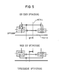
- the conductor tracks are arranged in such a way that a subsequent conductor track is adapted in its course to the contour of the previously determined conductor tracks in order to achieve a good use of space by this "snug" conductor track routing (see FIG. 2). Furthermore, the necessary contacts on the conductor tracks are arranged such that they are displaced with respect to the conductor tracks connected to them in such a way that they are pushed into an indentation contained in the adjacent conductor track in question in order to further improve the use of space.
- Automatic layout generation means that the dimensioning and arrangement of circuit elements and the associated definition of geometric structures are taken out of the hands of the designer and transferred to a program.
- a suitable language is required to describe geometric structures.
- the higher programming language Pascal which is supplemented by geometric primitives (embedded layout language)
- the procedural description enables the parameterization of the layout and a design rule independence.
- the content of the interface is checked for consistency. Among other things, the procedure determines whether all transistor electrodes are connected and whether lines have open ends.
- the basic cell individualization specified via the generator interface takes the form of an abstract network list.
- this network list In order to generate a concrete layout, this network list must be converted into a detailed circuit description. Therefore, a procedure has been implemented that generates the complete information about all required structures, e.g. Traces as connecting elements between nodes of the network list.
- Fig. 5 shows a typical starting situation and the result of the optimization.
- the geometric optimization begins.
- the coordinates of the vertical lines are determined first. This also includes topological information, e.g. about whether a contact is needed on a vertical line. After this step, the lines follow each other as closely as possible.
- the layout elements transistors, horizontal poly-Si tracks, contacts
- a flexible horizontal cell border was introduced, which shows the exact course of the upper limit of the placed structures. This border is differentiated according to layout levels. The margin is updated after each newly added structure. A horizontal trace is placed, for example, so that it "clings" to the current edge as much as possible. Jogs are generated automatically and in the right place. The jog procedure avoids nonsensical cable routing with unnecessarily deep and narrow gorges. This principle of structure placement is referred to as "layering" (Fig. 2).
- the flexible border is also taken into account when placing contacts.
- the placement routine then calculates the contact position in such a way that all adjacent contacts can be arranged in the most space-saving manner. However, contacts are not always placed as deeply as possible, since the length of the interconnect to be connected is also taken into account.
- Complete circuit modules are built from basic cells - the elements of the lowest hierarchy level of a module.
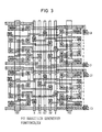
- 3 shows an exemplary embodiment of a subcircuit constructed from a multiplicity of the basic cell described above, as can be used in a bit-slice cell of a data path.
- the basic cell generation concept reduces the complexity associated with the design of VLSI layout.
- Basic cells the most elementary module components - allow automatic cell adaptation to the respective layout environment due to the numerous parameterization options and great flexibility.
- the procedural layout description leads to the independence of the module generator from the design rules of a certain manufacturing process. Algorithms for topological and geometric optimization ensure effective use of space.
- a simulator connection created in parallel to the generation of the layout permits rapid verification of the modules built up from basic cells.
- the basic cell described is tailored to data paths, but not in a function-specific manner. For certain applications, however, it makes sense to create a basic cell generator that is optimized for the circuit function to be designed (e.g. RAM, ROM).
- the advantages of high layout flexibility through procedural description also apply to such special basic cell generators.
Landscapes
- Engineering & Computer Science (AREA)
- Computer Hardware Design (AREA)
- Physics & Mathematics (AREA)
- Theoretical Computer Science (AREA)
- Evolutionary Computation (AREA)
- Geometry (AREA)
- General Engineering & Computer Science (AREA)
- General Physics & Mathematics (AREA)
- Design And Manufacture Of Integrated Circuits (AREA)
- Metal-Oxide And Bipolar Metal-Oxide Semiconductor Integrated Circuits (AREA)
- Internal Circuitry In Semiconductor Integrated Circuit Devices (AREA)
- Semiconductor Integrated Circuits (AREA)
Applications Claiming Priority (2)
| Application Number | Priority Date | Filing Date | Title |
|---|---|---|---|
| DE3518264 | 1985-05-21 | ||
| DE3518264 | 1985-05-21 |
Publications (2)
| Publication Number | Publication Date |
|---|---|
| EP0202573A2 true EP0202573A2 (fr) | 1986-11-26 |
| EP0202573A3 EP0202573A3 (fr) | 1989-07-19 |
Family
ID=6271268
Family Applications (1)
| Application Number | Title | Priority Date | Filing Date |
|---|---|---|---|
| EP86106433A Ceased EP0202573A3 (fr) | 1985-05-21 | 1986-05-12 | Cellule de base réalisée en technologie CMOS et procédé pour la configuration automatique d'une telle cellule |
Country Status (3)
| Country | Link |
|---|---|
| US (1) | US4783749A (fr) |
| EP (1) | EP0202573A3 (fr) |
| JP (1) | JPS61267346A (fr) |
Cited By (1)
| Publication number | Priority date | Publication date | Assignee | Title |
|---|---|---|---|---|
| CN104200049A (zh) * | 2014-09-22 | 2014-12-10 | 华北水利水电大学 | 一种评价建筑物移位技术可靠性的方法 |
Families Citing this family (9)
| Publication number | Priority date | Publication date | Assignee | Title |
|---|---|---|---|---|
| US5459673A (en) * | 1990-10-29 | 1995-10-17 | Ross Technology, Inc. | Method and apparatus for optimizing electronic circuits |
| US5566080A (en) * | 1993-09-07 | 1996-10-15 | Fujitsu Limited | Method and apparatus for designing semiconductor device |
| US5504694A (en) * | 1993-10-28 | 1996-04-02 | Motorola, Inc. | Method of cell characterization for energy dissipation |
| US5701255A (en) * | 1994-09-14 | 1997-12-23 | Matsushita Electric Industrial Co., Ltd. | Cell generation method and cell generation system |
| US5623420A (en) * | 1994-11-16 | 1997-04-22 | Sun Microsystems, Inc. | Method and apparatus to distribute spare cells within a standard cell region of an integrated circuit |
| US5631842A (en) * | 1995-03-07 | 1997-05-20 | International Business Machines Corporation | Parallel approach to chip wiring |
| US5877964A (en) * | 1997-01-10 | 1999-03-02 | International Business Machines Corporation | Semiconductor device compensation system and method |
| US6223331B1 (en) | 1998-07-30 | 2001-04-24 | Micron Technology, Inc. | Semiconductor circuit design method for employing spacing constraints and circuits thereof |
| US6493858B2 (en) * | 2001-03-23 | 2002-12-10 | The Board Of Trustees Of The Leland Stanford Jr. University | Method and system for displaying VLSI layout data |
Family Cites Families (7)
| Publication number | Priority date | Publication date | Assignee | Title |
|---|---|---|---|---|
| JPS5890758A (ja) * | 1981-11-25 | 1983-05-30 | Mitsubishi Electric Corp | 相補形集積回路装置 |
| IT1191188B (it) * | 1982-04-15 | 1988-02-24 | Cselt Centro Studi Lab Telecom | Cella elementare per reti di porte logiche a circuito integrato |
| JPS5943548A (ja) * | 1982-09-06 | 1984-03-10 | Hitachi Ltd | 半導体集積回路装置 |
| US4613940A (en) * | 1982-11-09 | 1986-09-23 | International Microelectronic Products | Method and structure for use in designing and building electronic systems in integrated circuits |
| JPS60152039A (ja) * | 1984-01-20 | 1985-08-10 | Toshiba Corp | GaAsゲ−トアレイ集積回路 |
| ATE53709T1 (de) * | 1984-06-19 | 1990-06-15 | Siemens Ag | In c-mos-technik realisierte basiszelle. |
| JPS61100947A (ja) * | 1984-10-22 | 1986-05-19 | Toshiba Corp | 半導体集積回路装置 |
-
1986
- 1986-04-15 US US06/852,159 patent/US4783749A/en not_active Expired - Fee Related
- 1986-05-12 EP EP86106433A patent/EP0202573A3/fr not_active Ceased
- 1986-05-16 JP JP61112415A patent/JPS61267346A/ja active Pending
Cited By (2)
| Publication number | Priority date | Publication date | Assignee | Title |
|---|---|---|---|---|
| CN104200049A (zh) * | 2014-09-22 | 2014-12-10 | 华北水利水电大学 | 一种评价建筑物移位技术可靠性的方法 |
| CN104200049B (zh) * | 2014-09-22 | 2017-11-17 | 华北水利水电大学 | 一种评价建筑物移位技术可靠性的方法 |
Also Published As
| Publication number | Publication date |
|---|---|
| US4783749A (en) | 1988-11-08 |
| JPS61267346A (ja) | 1986-11-26 |
| EP0202573A3 (fr) | 1989-07-19 |
Similar Documents
| Publication | Publication Date | Title |
|---|---|---|
| DE3650323T2 (de) | VLSI-Chip und Verfahren zur Herstellung. | |
| DE69722425T2 (de) | Verfahren und vorrichtung zum routing von netzen in einem elektronischen gerät | |
| EP0441810B1 (fr) | Procede pour placer des modules sur un support | |
| DE69521507T2 (de) | System und verfahren zur auf einem modell basierender prüfung von lokalen entwurfsregeln | |
| EP0855662B1 (fr) | Analyse électrique des circuits integrés | |
| DE10025583A1 (de) | Verfahren zur Optimierung integrierter Schaltungen, Vorrichtung zum Entwurf von Halbleitern und Programmobjekt zum Entwerfen integrierter Schaltungen | |
| DE68921550T2 (de) | Verfahren und Gerät zur Bildung eines Pattern-Layouts einer integrierten Halbleiterschaltung. | |
| DE68929212T2 (de) | Verfahren zur Zuteilung von Ebenen unter Knoten in einem Netzdiagramm | |
| DE2936915C2 (de) | Verfahren und Vorrichtung zur Steuerung eines Ein-Aus-Anzeige-Wählsignals in einer Anzeige- und Ablaufsteuerung | |
| DE69433907T2 (de) | Autonomes, evolutionsartiges Hardwareentwurfssystem | |
| DE69517693T2 (de) | Standardzellenbibliothek für den Entwurf von integrierten Schaltungen | |
| DE3872737T2 (de) | Verfahren zur kombinierung von "gate array"-schaltungen mit standardschaltungen auf ein gemeinsames halbleiterplaettchen. | |
| EP0202573A2 (fr) | Cellule de base réalisée en technologie CMOS et procédé pour la configuration automatique d'une telle cellule | |
| DE2442850A1 (de) | Verfahren zum automatischen design integrierter schaltungen | |
| DE4128568A1 (de) | Mehrschichten-verdrahtungsverfahren zur modifikation am chip fuer einen hochintegrierten halbleiterschaltkreis (lsi) | |
| DE69426507T2 (de) | System und Verfahren zur gleichzeitigen Prozess- und Device-Simulation | |
| DE4327652C2 (de) | Integrierte Halbleiterschaltungsvorrichtung und Verfahren zum Entwerfen einer integrierten Halbleiterschaltungsvorrichtung | |
| EP0166027B1 (fr) | Cellule élémentaire réalisée en technique C-MOS | |
| DE10205559B4 (de) | Integrierte Schaltung und Verfahren und Vorrichtung zum Entwurf einer integrierten Schaltung | |
| DE10138142A1 (de) | Verfahren zur Analyse einer integrierten elektrischen Schaltung | |
| EP1146393B1 (fr) | Procédé pour réaliser des photomasques pour la production des structures sur semi-conducteurs | |
| DE10238051B4 (de) | Integrierte Flip-Chip-Halbleiterschaltung | |
| DE4327290C2 (de) | Integrierte Halbleiterschaltung | |
| DE10317924A1 (de) | Layoutentwurfsverfahren und System zum Liefern einer Umgehungskapazität und einer konformen Dichte in einer integrierten Schaltung | |
| DE10164424A1 (de) | Elektrische oder elektronische Schaltungsanordnung sowie zugeordnetes Verfahren |
Legal Events
| Date | Code | Title | Description |
|---|---|---|---|
| PUAI | Public reference made under article 153(3) epc to a published international application that has entered the european phase |
Free format text: ORIGINAL CODE: 0009012 |
|
| AK | Designated contracting states |
Kind code of ref document: A2 Designated state(s): AT CH DE FR GB LI |
|
| PUAL | Search report despatched |
Free format text: ORIGINAL CODE: 0009013 |
|
| AK | Designated contracting states |
Kind code of ref document: A3 Designated state(s): AT CH DE FR GB LI |
|
| RHK1 | Main classification (correction) |
Ipc: H01L 27/02 |
|
| 17P | Request for examination filed |
Effective date: 19890808 |
|
| R17P | Request for examination filed (corrected) |
Effective date: 19890808 |
|
| 17Q | First examination report despatched |
Effective date: 19910612 |
|
| STAA | Information on the status of an ep patent application or granted ep patent |
Free format text: STATUS: THE APPLICATION HAS BEEN REFUSED |
|
| 18R | Application refused |
Effective date: 19921019 |
|
| RIN1 | Information on inventor provided before grant (corrected) |
Inventor name: SCHALLENBERGER, BURGHARDT, DR. Inventor name: DUZY, PETER, DIPL.-ING. Inventor name: DE MARINO, RALF, DIPL.-ING. |