EP0203422A2 - Circuit de sélection à trois états destiné à un système de traitement de données - Google Patents
Circuit de sélection à trois états destiné à un système de traitement de données Download PDFInfo
- Publication number
- EP0203422A2 EP0203422A2 EP86106182A EP86106182A EP0203422A2 EP 0203422 A2 EP0203422 A2 EP 0203422A2 EP 86106182 A EP86106182 A EP 86106182A EP 86106182 A EP86106182 A EP 86106182A EP 0203422 A2 EP0203422 A2 EP 0203422A2
- Authority
- EP
- European Patent Office
- Prior art keywords
- transistor
- output
- current switch
- circuit
- select
- Prior art date
- Legal status (The legal status is an assumption and is not a legal conclusion. Google has not performed a legal analysis and makes no representation as to the accuracy of the status listed.)
- Withdrawn
Links
Images


Classifications
-
- H—ELECTRICITY
- H03—ELECTRONIC CIRCUITRY
- H03K—PULSE TECHNIQUE
- H03K19/00—Logic circuits, i.e. having at least two inputs acting on one output; Inverting circuits
- H03K19/02—Logic circuits, i.e. having at least two inputs acting on one output; Inverting circuits using specified components
- H03K19/173—Logic circuits, i.e. having at least two inputs acting on one output; Inverting circuits using specified components using elementary logic circuits as components
- H03K19/1733—Controllable logic circuits
- H03K19/1738—Controllable logic circuits using cascode switch logic [CSL] or cascode emitter coupled logic [CECL]
-
- H—ELECTRICITY
- H03—ELECTRONIC CIRCUITRY
- H03K—PULSE TECHNIQUE
- H03K19/00—Logic circuits, i.e. having at least two inputs acting on one output; Inverting circuits
- H03K19/02—Logic circuits, i.e. having at least two inputs acting on one output; Inverting circuits using specified components
- H03K19/08—Logic circuits, i.e. having at least two inputs acting on one output; Inverting circuits using specified components using semiconductor devices
- H03K19/082—Logic circuits, i.e. having at least two inputs acting on one output; Inverting circuits using specified components using semiconductor devices using bipolar transistors
- H03K19/0823—Multistate logic
- H03K19/0826—Multistate logic one of the states being the high impedance or floating state
Definitions
- Three state current switch emitter follower gate circuits for providing a differential output state or an inhibit state under control of a selectldeselect signal are well known in the art.
- the differential output state facilitates the employment of a differential bus in data processing equipment such as directory memory systems.
- the advantages of a differential bus over a single ended bus are to a significant degree offset by the increased power and delay of the differential output gate circuits of the prior art.
- the tri-state current switch emitter follower gate circuit in accordance with the invention provides the advantages of differential bussing without incurring the power consuming penalty inherent in prior art differential output gate circuits.
- the present invention has particular utility and advantage when employed in a directory memory system for use in a data processing system having a cache memory, and more particularly to a directory memory system formed in a monolithic integrated circuit having the capability of performing simultaneous write/ compare, read/compare, compare/bypass, write/bypass, or write/compare/bypass operations.
- Directory memory systems particularly directory memory systems fabricated in a single integrated circuit chip, have recently found increasing use in high-speed data processing systems.
- a directory memory system is described in U.S. Patent No. 4,219,883 to Kobayashi et al.
- Such devices can be used advantageously to perform a number of different functions within the data processing system.
- a cache memory which is a small, high-speed memory functionally positioned between a main, slower memory and a central processor.
- the cache memory stores the most frequently used data retrieved by the processor from the main memory for rapid access by the processor.
- Another application of a directory memory is in a "trace" system in which a predetermined amount of the data most recently used by the processor is stored for examination to locate possible faults within the data processing system. Many other applications, of course, are possible.
- a directory memory system should generally have the capability of performing the functions of writing input data into a memory block for temporary storage therein, reading data from the memory block onto an output data bus, comparing designated portions of the data stored in the memory block with comparison data, and bypassing the comparison data onto the output data bus under certain conditions.
- the capabilities of directory memories are further enhanced by dividing the memory block array into two or more subarrays which are addressable either individually or in various combinations.
- Directory memories which store and compare addresses associated with main and cache memories, and which have a memory array divided into two or more subarrays are well known. Typical systems are disclosed in U.S. Patent Nos. 3,685,020 to Meade, 3,723,976 to Alvarez et al., 3,761,881 to Anderson et at., 4,044,338 to Wolf, 4,136,385 to Gannon et al., and 4,332,010 to Messina et al. Memory systems having two or more subarrays which are reconfigurable for write and/or read operations are disclosed in U.S. Patent Nos.
- a directory memory system including a simultaneous write and bypass function is disclosed in copending European Patent Application No. 0 130 414, cited above, and a logic circuit having a bypass circuit therein is described in U.S. Patent No. 4,286,173 to Oka et al.
- the directory system select circuit is in this path, therefore it is desirable to reduce the select circuit delay as much as possible. Additionally the select circuit is replicated many times on a directory chip, typically if is the 3rd most numerous circuit after the cell and compare circuit. Therefore it is advantageous to be able to have the circuit layout as small as possible.
- Prior art circuits that have a single ended output provide small layout but do not have the symetrical switching characteristics of differential select circuits and require a tracking ref. These desirable characteristics are smaller signal swings for better performance, better common mode noise immunity and no read 0/read 1 delay skew.
- Prior art differential circuits employed cumbersome means for providing the negative inhibit.
- the negative inhibit implementations added delay, area and power due to inverter stages placed between the current switch and the emitter follower outputs, or additional current means for inhibit.
- Prior art circuits incorporating three state select without cascode are not suited for directory chip bit select requirements due to input level incompatibility with sense amp and byte decode output levels. These circuits without cascode will not allow simultaneous write/bypass. Also implementation of tri-level switching inputs is required of three state select circuits without cascode. Tri-level switching inputs require large signal swings which cause increased delay as well as poor signal margin.
- the invention may be summarized as three state cascode current switch select circuit for controllably receiving a binary input and providing a binary output, said cascode current switch select circuit including: interconnected upper and lower current switch circuits; said lower current switch including a control input adapted to receive a signal for placing said cascode current switch circuit means in either a SELECT state or a DESELECT state; and said cascode current switch select circuit being characterized by the inclusion of power reduction circuit means interconnecting said upper and lower current switch circuits, whereby the power consumption of said cascode current switch select circuit is reduced.
- the invention may also be summarized as data bit selection means, for use in a data processing system, such as a directory memory system or the like, said data bit selection means comprising: a plurality of data bit select circuits, each of said data bit select circuits having a data bit true input terminal and a data bit complement input terminal, a data bit true output terminal and a data bit complement output terminal, and a deselect/select con- trot terminal, a first true bus connected in common to each of said data bit true output terminals of said data bit select circuits; a second complement bus connected in common to each of said data complement output terminals; and, each of said data bit select circuits comprising cascode current switch circuit means having at least interconnected upper and lower current switch circuit means; each of said data bit select circuits being characterized by power reduction circuit means coupling said lower current switch circuit means to said true and complement data bit output terminals of said data bit select circuit.
- a three state C.S.E.F. gate with differential output and negative inhibit has been implemented in the past. See Figures 1 and 2.
- the advantages of a differential bus over a single ended bus are offset by the increased power and delay of these circuits.
- the circuit in accordance with the invention, Fig. 4 provides the advantages of differential bussing without the extra power of prior art circuits and better performance than a single ended gate.
- the employment of the circuit in accordance with the invention in a memory systems provides a differential data bus and eliminates read 0/read 1 skew and the problems inherent with generating a tracking reference.
- current l cs is provided by a standard current source such as a current mirror.
- T s When the select line is high (deselect) T s is on and T. is off.
- Schottky diodes D 3 and D 4 share current I cs , and I cs /2 flows through each of the resistors R3 and R4, thus the bases of emitter followers T 3 and T 4 are respectively at a low voltage.
- the circuit is disabled (deselected).
- T 6 When the select line is low T 6 is on, T s is off and either T, or T 2 is on depending on the input data. If T 2 is on and T, is off, output DB is high because no current flows through R, and R3. I cs /2 current flows through R 2 and R. and Schottky diode D 2 so DB is low.
- V FD1 is the forward voltage drop across Schottky diode 1.
- I cs divides evenly between diodes 3 and 4. Therefore I cs/2 flows through R3 and R4 and the bases of T3 and T4 are at a low voltage.
- I cs/2 In order to achieve the same low state voltage level at the bases of T3 and T4 when in select state as in deselect state, I cs/2 must flow through either D, and R 3 or D2 and R4 depending on input data when selected.
- I cs sets the total power in all modes of operation. Extra power for inverters or deselect is not needed as in the circuit of Fig. 1. In addition one state of delay (inverter) is eliminated.
- a differential data bus has performance and symmetrical switching advantages over a single ended bus (no read ⁇ /read 1 skew).
- the emitter follower dot is used in the implementation of the data bus; however, the emitter follower dot requires negative inhibit.
- the disclosed select gate of figure 4 solves this problem with minimum delay and power in C.S.E.F. logic.
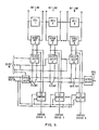
- Figure 5 shows of a portion of a directory array chip.
- a single memory cell is shown for illustration; however, any number of cells may be implemented. It is necessary to have array data from cell 1, cell 2 or cell N or a compare data bit appear at the data out. Simultaneously array data from cell 1, cell 2 or cell N must appear at the input to their respective compare circuits to generate compare status signals 1, 2, and N. Choice of cell 1 data, cell 2 data, cell N data or compare data, at the data output is made via select input lines 1, 2, N or B.
- the function of the select gate is to inhibit its corresponding cell data bit from interfering with the data bus when another cell data bit or compare data bit is desired at the data output.
- the function of the bypass gate is to inhibit the compare data bit from interfering with the data bus when cell data is desired at the data output.
- Select gate-1, select gate 2 select gate-N and the bypass gate are identical; and each correspond identically to select circuit shown in figure 4. Operation of the select gate circuit of figure 4 has been explained earlier herein.
- each select gate circuit Fig. 4 must fit within the bit pitch of one array cell in the physical design.
- the select circuit offers a compact layout because Schottky diodes 3 and 4 are integrated in the same collector as T s . Similar Schottky diode D1 is integrated with T, and Schottky D2 is integrated with T 2-
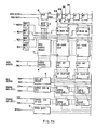
- a directory array is organized into eight subarrays. Each subarray is ten bits wide and thirty-two bits high. During a read operation one wordline containing eight ten bit 'bytes' is selected.
- the chip architecture requires array data to follow two paths. All eight bytes (eighty bits) of the selected word must appear at the compare logic inputs (not shown) for the compare function. Also one of the eight bytes is selected via byte decode inputs to be driven off chip. Since one byte must be fed to the data output drivers the chip has a ten bit wide data bus requirement.
- the chip has a bypass function where ten bits coming from off chip (called compare data input byte) can be steered onto the data bus to appear at the data outputs in lieu of array data. See figure 6.
- a differential data bus has performance and symmetrical switching advantages over a single ended bus (no read 0/read 1 skew).
- a differential select circuit as disclosed offers several advantages over a single ended select circuit, figure 3.
- the differential circuit allows a smaller signal swing, therefore obtaining faster switching times and better performance.
- the differential circuit rejects common mode noise. Noise on the most positive power supply propagates to both the low and high level bus lines therefore no false switching occurs at receiving circuit. With a single ended circuit the noise may propagate to the bus, but not to the reference which could be far away from the circuit. Therefore false switching may occur.
- the differential circuit Compared to the single ended circuit, the differential circuit has reduced on chip generated delta I noise when changing the state of input data.
- the directory chip may have typically 10 of these circuits active. Any data change with the differential circuit will not cause local high current demands because of the complementary outputs' cancelling effect.
- Ten single ended circuits all changing from a '0' to '1' state may cause current glitches in the most positive power supply.
- the single ended circuit will have delay skew between selecting a '1' or a '0'. Switching around a fixed reference, the emitter follower has different delay between going from a '0' to a '1' through the reference voltage, and vice versa.
- the symetrical nature of the differential circuit and absence of a switching reference eliminates this skew.
- the disclosed circuit provides negative inhibit and differential output, and is desirably used for the byte select and bypass gate functions on a directory chip.
- the lower portion of the cascode in the circuit of figure 3 receives the select signal from the byte decode circuitry and the upper portion receives data from the array sense amplifiers.
- the lower cascode receives a select signal from the bypass receiver and the upper portion receives data from the compare data input receivers.
- the input voltage level requirements of the disclosed circuit are compatible array circuit families and power supplies. Therefore the output levels of the sense amplifiers and byte decode circuits match the input levels of the disclosed circuit.
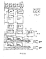
- Figure 7 formed by joining figures 7A and 7B of the present patent application correspond identically to figures 1A and 1B of European Patent Application No. 0 180 022. It will be apparent, in view of the foregoing explanation that the select circuit of figure 4 finds particular utility when employed in a directory memory system of the type and as shown in the block diagram of figure 7.
Landscapes
- Engineering & Computer Science (AREA)
- Physics & Mathematics (AREA)
- Computer Hardware Design (AREA)
- Computing Systems (AREA)
- General Engineering & Computer Science (AREA)
- Mathematical Physics (AREA)
- Power Engineering (AREA)
- Static Random-Access Memory (AREA)
- Electronic Switches (AREA)
- Logic Circuits (AREA)
Applications Claiming Priority (2)
| Application Number | Priority Date | Filing Date | Title |
|---|---|---|---|
| US739785 | 1985-05-31 | ||
| US06/739,785 US4636990A (en) | 1985-05-31 | 1985-05-31 | Three state select circuit for use in a data processing system or the like |
Publications (2)
| Publication Number | Publication Date |
|---|---|
| EP0203422A2 true EP0203422A2 (fr) | 1986-12-03 |
| EP0203422A3 EP0203422A3 (fr) | 1988-08-03 |
Family
ID=24973770
Family Applications (1)
| Application Number | Title | Priority Date | Filing Date |
|---|---|---|---|
| EP86106182A Withdrawn EP0203422A3 (fr) | 1985-05-31 | 1986-05-06 | Circuit de sélection à trois états destiné à un système de traitement de données |
Country Status (4)
| Country | Link |
|---|---|
| US (1) | US4636990A (fr) |
| EP (1) | EP0203422A3 (fr) |
| JP (1) | JPS61278208A (fr) |
| CA (1) | CA1255808A (fr) |
Families Citing this family (11)
| Publication number | Priority date | Publication date | Assignee | Title |
|---|---|---|---|---|
| US4682058A (en) * | 1986-07-03 | 1987-07-21 | Unisys Corporation | Three-state logic circuit for wire-ORing to a data bus |
| US4845387A (en) * | 1987-05-28 | 1989-07-04 | Texas Instruments Incorporated | Non-stacked ECL type and function |
| JPH0817319B2 (ja) * | 1987-09-24 | 1996-02-21 | 株式会社日立製作所 | 3ステート回路及びそれを用いた出力回路 |
| EP0426597B1 (fr) * | 1989-10-30 | 1995-11-08 | International Business Machines Corporation | Schéma de décodage par bit pour réseaux de mémoire |
| US5022010A (en) * | 1989-10-30 | 1991-06-04 | International Business Machines Corporation | Word decoder for a memory array |
| WO1991018394A1 (fr) * | 1990-05-17 | 1991-11-28 | International Business Machines Corporation | Circuit de lecture/ecriture/remise a l'etat initial pour reseaux de memoire |
| JPH04258876A (ja) * | 1991-02-12 | 1992-09-14 | Mitsubishi Electric Corp | 半導体メモリ装置およびメモリアクセスシステム |
| JP2611725B2 (ja) * | 1993-09-13 | 1997-05-21 | 日本電気株式会社 | カスコード回路 |
| US5914906A (en) | 1995-12-20 | 1999-06-22 | International Business Machines Corporation | Field programmable memory array |
| KR100778355B1 (ko) | 2005-08-22 | 2007-11-22 | 미쓰비시덴키 가부시키가이샤 | 캐스코드 접속회로 |
| TWI902513B (zh) * | 2024-10-30 | 2025-10-21 | 大陸商北京集創北方科技股份有限公司 | 三態輸入端口電路、電子晶片及資訊處理裝置 |
Family Cites Families (26)
| Publication number | Priority date | Publication date | Assignee | Title |
|---|---|---|---|---|
| US3471838A (en) * | 1965-06-21 | 1969-10-07 | Magnavox Co | Simultaneous read and write memory configuration |
| US3590274A (en) * | 1969-07-15 | 1971-06-29 | Fairchild Camera Instr Co | Temperature compensated current-mode logic circuit |
| US3622799A (en) * | 1970-04-20 | 1971-11-23 | Fairchild Camera Instr Co | Temperature-compensated current-mode circuit |
| US3685020A (en) * | 1970-05-25 | 1972-08-15 | Cogar Corp | Compound and multilevel memories |
| US3686640A (en) * | 1970-06-25 | 1972-08-22 | Cogar Corp | Variable organization memory system |
| US3761898A (en) * | 1971-03-05 | 1973-09-25 | Raytheon Co | Random access memory |
| US3761881A (en) * | 1971-06-30 | 1973-09-25 | Ibm | Translation storage scheme for virtual memory system |
| US3723976A (en) * | 1972-01-20 | 1973-03-27 | Ibm | Memory system with logical and real addressing |
| US3800289A (en) * | 1972-05-15 | 1974-03-26 | Goodyear Aerospace Corp | Multi-dimensional access solid state memory |
| US3787817A (en) * | 1972-06-21 | 1974-01-22 | Us Navy | Memory and logic module |
| US4087853A (en) * | 1973-11-20 | 1978-05-02 | Casio Computer Co., Ltd. | Storage reconfiguration apparatus |
| US3925691A (en) * | 1974-03-11 | 1975-12-09 | Hughes Aircraft Co | Cascode node idle current injection means |
| US3955099A (en) * | 1974-03-11 | 1976-05-04 | Hughes Aircraft Company | Diode controlled idle current injection |
| US3958222A (en) * | 1974-06-27 | 1976-05-18 | Ibm Corporation | Reconfigurable decoding scheme for memory address signals that uses an associative memory table |
| AT354159B (de) * | 1975-02-10 | 1979-12-27 | Siemens Ag | Assoziativspeicher mit getrennt assoziierbaren bereichen |
| US4075686A (en) * | 1976-12-30 | 1978-02-21 | Honeywell Information Systems Inc. | Input/output cache system including bypass capability |
| US4070657A (en) * | 1977-01-03 | 1978-01-24 | Honeywell Information Systems Inc. | Current mode simultaneous dual-read/single-write memory device |
| US4136385A (en) * | 1977-03-24 | 1979-01-23 | International Business Machines Corporation | Synonym control means for multiple virtual storage systems |
| US4286173A (en) * | 1978-03-27 | 1981-08-25 | Hitachi, Ltd. | Logical circuit having bypass circuit |
| JPS54128634A (en) * | 1978-03-30 | 1979-10-05 | Toshiba Corp | Cash memory control system |
| US4268907A (en) * | 1979-01-22 | 1981-05-19 | Honeywell Information Systems Inc. | Cache unit bypass apparatus |
| US4222112A (en) * | 1979-02-09 | 1980-09-09 | Bell Telephone Laboratories, Incorporated | Dynamic RAM organization for reducing peak current |
| US4241425A (en) * | 1979-02-09 | 1980-12-23 | Bell Telephone Laboratories, Incorporated | Organization for dynamic random access memory |
| US4332010A (en) * | 1980-03-17 | 1982-05-25 | International Business Machines Corporation | Cache synonym detection and handling mechanism |
| US4490630A (en) * | 1982-06-30 | 1984-12-25 | International Business Machines Corporation | Current switch emitter follower with current mirror coupled push-pull output stage |
| US4596002A (en) * | 1984-06-25 | 1986-06-17 | International Business Machines Corporation | Random access memory RAM employing complementary transistor switch (CTS) memory cells |
-
1985
- 1985-05-31 US US06/739,785 patent/US4636990A/en not_active Expired - Fee Related
-
1986
- 1986-03-18 JP JP61058462A patent/JPS61278208A/ja active Pending
- 1986-04-22 CA CA000507290A patent/CA1255808A/fr not_active Expired
- 1986-05-06 EP EP86106182A patent/EP0203422A3/fr not_active Withdrawn
Also Published As
| Publication number | Publication date |
|---|---|
| JPS61278208A (ja) | 1986-12-09 |
| EP0203422A3 (fr) | 1988-08-03 |
| CA1255808A (fr) | 1989-06-13 |
| US4636990A (en) | 1987-01-13 |
Similar Documents
| Publication | Publication Date | Title |
|---|---|---|
| KR930006843B1 (ko) | 반도체 집적회로 | |
| US4817051A (en) | Expandable multi-port random access memory | |
| US4193127A (en) | Simultaneous read/write cell | |
| US4608672A (en) | Semiconductor memory | |
| US4961164A (en) | Semiconductor memory device with dual selection circuitry including CMOS and bipolar transistors | |
| EP0023792B1 (fr) | Mémoire à semi-conducteurs comprenant des cellules intégrées à injection logique | |
| US4636990A (en) | Three state select circuit for use in a data processing system or the like | |
| US3919566A (en) | Sense-write circuit for bipolar integrated circuit ram | |
| US4348747A (en) | System for driving bipolar ram | |
| US4694433A (en) | Semiconductor memory having subarrays and partial word lines | |
| US4651302A (en) | Read only memory including an isolation network connected between the array of memory cells and the output sense amplifier whereby reading speed is enhanced | |
| US4757475A (en) | Semiconductor memory device having diode matrix type decoder and redundancy configuration | |
| EP0130414B1 (fr) | Mémoire de table de matières | |
| EP0090186B1 (fr) | Circuit logique complémentaire | |
| US4520462A (en) | Semiconductor memory device | |
| US4910711A (en) | Bicmos read/write control and sensing circuit | |
| US3540002A (en) | Content addressable memory | |
| US4592023A (en) | Latch for storing a data bit and a store incorporating said latch | |
| US4456979A (en) | Static semiconductor memory device | |
| EP0023408B1 (fr) | Mémoire à semi-conducteurs comprenant des cellules intégrées à injection logique | |
| US4138739A (en) | Schottky bipolar two-port random-access memory | |
| US4593383A (en) | Integated circuit memory | |
| JPH0777075B2 (ja) | デコーダ−ドライバ回路 | |
| US4791382A (en) | Driver circuit | |
| US3703711A (en) | Memory cell with voltage limiting at transistor control terminals |
Legal Events
| Date | Code | Title | Description |
|---|---|---|---|
| PUAI | Public reference made under article 153(3) epc to a published international application that has entered the european phase |
Free format text: ORIGINAL CODE: 0009012 |
|
| AK | Designated contracting states |
Kind code of ref document: A2 Designated state(s): DE FR GB IT |
|
| 17P | Request for examination filed |
Effective date: 19870327 |
|
| PUAL | Search report despatched |
Free format text: ORIGINAL CODE: 0009013 |
|
| AK | Designated contracting states |
Kind code of ref document: A3 Designated state(s): DE FR GB IT |
|
| 17Q | First examination report despatched |
Effective date: 19900727 |
|
| STAA | Information on the status of an ep patent application or granted ep patent |
Free format text: STATUS: THE APPLICATION HAS BEEN WITHDRAWN |
|
| 18W | Application withdrawn |
Withdrawal date: 19920828 |
|
| RIN1 | Information on inventor provided before grant (corrected) |
Inventor name: BUSCAGLIA, CARL UGO Inventor name: KNEPPER, LAWRENCE EDWARD |