EP0205148A2 - Procédé d'application de réserves - Google Patents
Procédé d'application de réserves Download PDFInfo
- Publication number
- EP0205148A2 EP0205148A2 EP86107872A EP86107872A EP0205148A2 EP 0205148 A2 EP0205148 A2 EP 0205148A2 EP 86107872 A EP86107872 A EP 86107872A EP 86107872 A EP86107872 A EP 86107872A EP 0205148 A2 EP0205148 A2 EP 0205148A2
- Authority
- EP
- European Patent Office
- Prior art keywords
- resist
- applying
- thickness
- pattern
- photoresist
- Prior art date
- Legal status (The legal status is an assumption and is not a legal conclusion. Google has not performed a legal analysis and makes no representation as to the accuracy of the status listed.)
- Granted
Links
Images


Classifications
-
- G—PHYSICS
- G03—PHOTOGRAPHY; CINEMATOGRAPHY; ANALOGOUS TECHNIQUES USING WAVES OTHER THAN OPTICAL WAVES; ELECTROGRAPHY; HOLOGRAPHY
- G03F—PHOTOMECHANICAL PRODUCTION OF TEXTURED OR PATTERNED SURFACES, e.g. FOR PRINTING, FOR PROCESSING OF SEMICONDUCTOR DEVICES; MATERIALS THEREFOR; ORIGINALS THEREFOR; APPARATUS SPECIALLY ADAPTED THEREFOR
- G03F7/00—Photomechanical, e.g. photolithographic, production of textured or patterned surfaces, e.g. printing surfaces; Materials therefor, e.g. comprising photoresists; Apparatus specially adapted therefor
- G03F7/16—Coating processes; Apparatus therefor
- G03F7/162—Coating on a rotating support, e.g. using a whirler or a spinner
-
- G—PHYSICS
- G03—PHOTOGRAPHY; CINEMATOGRAPHY; ANALOGOUS TECHNIQUES USING WAVES OTHER THAN OPTICAL WAVES; ELECTROGRAPHY; HOLOGRAPHY
- G03F—PHOTOMECHANICAL PRODUCTION OF TEXTURED OR PATTERNED SURFACES, e.g. FOR PRINTING, FOR PROCESSING OF SEMICONDUCTOR DEVICES; MATERIALS THEREFOR; ORIGINALS THEREFOR; APPARATUS SPECIALLY ADAPTED THEREFOR
- G03F7/00—Photomechanical, e.g. photolithographic, production of textured or patterned surfaces, e.g. printing surfaces; Materials therefor, e.g. comprising photoresists; Apparatus specially adapted therefor
- G03F7/20—Exposure; Apparatus therefor
-
- G—PHYSICS
- G03—PHOTOGRAPHY; CINEMATOGRAPHY; ANALOGOUS TECHNIQUES USING WAVES OTHER THAN OPTICAL WAVES; ELECTROGRAPHY; HOLOGRAPHY
- G03F—PHOTOMECHANICAL PRODUCTION OF TEXTURED OR PATTERNED SURFACES, e.g. FOR PRINTING, FOR PROCESSING OF SEMICONDUCTOR DEVICES; MATERIALS THEREFOR; ORIGINALS THEREFOR; APPARATUS SPECIALLY ADAPTED THEREFOR
- G03F7/00—Photomechanical, e.g. photolithographic, production of textured or patterned surfaces, e.g. printing surfaces; Materials therefor, e.g. comprising photoresists; Apparatus specially adapted therefor
- G03F7/26—Processing photosensitive materials; Apparatus therefor
- G03F7/30—Imagewise removal using liquid means
-
- Y—GENERAL TAGGING OF NEW TECHNOLOGICAL DEVELOPMENTS; GENERAL TAGGING OF CROSS-SECTIONAL TECHNOLOGIES SPANNING OVER SEVERAL SECTIONS OF THE IPC; TECHNICAL SUBJECTS COVERED BY FORMER USPC CROSS-REFERENCE ART COLLECTIONS [XRACs] AND DIGESTS
- Y10—TECHNICAL SUBJECTS COVERED BY FORMER USPC
- Y10S—TECHNICAL SUBJECTS COVERED BY FORMER USPC CROSS-REFERENCE ART COLLECTIONS [XRACs] AND DIGESTS
- Y10S430/00—Radiation imagery chemistry: process, composition, or product thereof
- Y10S430/136—Coating process making radiation sensitive element
Definitions
- the present invention relates to a method of applying a resist, and particularly to a method of applying a resist that is adapted for a process for producing highly integrated circuit elements where little variation is allowed in the size of the developed pattern.
- a method of applying a resist has been disclosed in Japanese Patent Laid-Open No. 155925/1984. According to this method, the photosensitive reaction is effected prior to applying the resist. However, nothing has been referred to in regard to optimizing the film thickness of the resist. Further, Japanese Patent Laid-Open Nos. 155930/1984, 155927/1984 and 155921/1984 disclose methods of applying a resist in relation to forming fine patterns. However, none of them teach to optimize the film thickness of the resist.
- the object of the present invention is to provide a method of applying a resist, which is capable of increasing the production yields of highly integrated circuit elements while decreasing the variance in the developing size of elements formed on the silicon wafers.
- the resist size width kr of resist line 6 of Fig. 2, which should desirably be equal to the line width km of a mask pattern which consists of a line portion 4 and a space portion 5) after developing pulsates as represented by a curve 3 in Fig. 1.
- a process for forming the resist line 6 on a silicon substrate 7 will be described below in conjunction with Fig. 3. First, the silicon substate 7 is spin-coated with a resist 10 to a thickness of about 1 ⁇ m.
- a projected image of mask pattern consisting of space portion and line portion is then irradiated with a source of ultraviolet rays.
- the intensity of light on the resist 10 is weak at a position which corresponds to the line portion and is strong at a position which corresponds to the space portion, as represented by a curve 9.
- the resist melts at a portion which corresponds to the strongly irradiated space portion 5.
- the resist at a portion corresponding to the weakly irradiated line portion 4 does not melt but remains to form the resist line 6 shown in Fig. 2.
- a resist line is formed at a portion that corresponds to the space portion.
- the film thickness does not become uniform but varies by about 200 angstroms. Therefore, variance develops in the width of resist line that is formed after developing.
- the range of variance of the line width greatly changes depending upon the set point (central value in the variance of resist film thickenss) of the thickness of resist film. For instance, if the thickness of the resist film is denoted by t 3 , the film thickness varies over a range ⁇ t; consequently, the developed pattern varies over a range ⁇ l 3 . However, if the thickness of the resist film is set to t 2 which corresponds to a minimum value of the curve 3, the developed pattern varies over a range ⁇ l 2 despite the thickness of the resist film varing over the same range ⁇ t, which is a reduction into about one-fifth from the range ⁇ l 3 .
- the developing size varies over a range ⁇ l 1 , which is a reduction into about one-fifth from the range ⁇ l 3 .
- the range ⁇ l 3 generally has a value of 0.3 ⁇ m. This value becomes intolerable as the resist size approaches 1 ⁇ m.
- the allowable value of variance in the developing size is ⁇ l with respect to the design size ld in the photoresist process for producing semiconductor elements.
- the setpoint of thickness of the resist film is erroneously set to t 3 in Fig. 1, the size of the developed pattern greatly, and the number of semiconductor elements relative to the developed pattern is distributed as represented by a curve 11.
- Many elements (those denoted by 12, 13) that lie outside the allowable pattern ld ⁇ ⁇ l become defective.
- variance in the developed pattern decreases as represented by a curve 14, and the proportion of defective elements decreses to less than 10% as distributed in the portions denoted by 15 and 16.
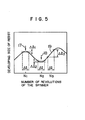
- the developed pattern varies little as denoted by ⁇ l 1 and ⁇ l 2 when the number of revolutions N l , N 2 correspond to extreme values 17, 18 even though the thickness of the resist film varies over the same range At as that of Fig. 1.
- the developed pattern varies over an increased range ⁇ l 3 .
- Fig. 4 is a diagram which illustrates the variance in the developing size.
Landscapes
- Physics & Mathematics (AREA)
- General Physics & Mathematics (AREA)
- Exposure Of Semiconductors, Excluding Electron Or Ion Beam Exposure (AREA)
- Application Of Or Painting With Fluid Materials (AREA)
- Formation Of Insulating Films (AREA)
- Photosensitive Polymer And Photoresist Processing (AREA)
- Exposure And Positioning Against Photoresist Photosensitive Materials (AREA)
Applications Claiming Priority (2)
| Application Number | Priority Date | Filing Date | Title |
|---|---|---|---|
| JP126133/85 | 1985-06-12 | ||
| JP60126133A JPS61285716A (ja) | 1985-06-12 | 1985-06-12 | レジスト塗布方法 |
Publications (3)
| Publication Number | Publication Date |
|---|---|
| EP0205148A2 true EP0205148A2 (fr) | 1986-12-17 |
| EP0205148A3 EP0205148A3 (en) | 1988-12-28 |
| EP0205148B1 EP0205148B1 (fr) | 1991-04-24 |
Family
ID=14927484
Family Applications (1)
| Application Number | Title | Priority Date | Filing Date |
|---|---|---|---|
| EP86107872A Expired - Lifetime EP0205148B1 (fr) | 1985-06-12 | 1986-06-10 | Procédé d'application de réserves |
Country Status (6)
| Country | Link |
|---|---|
| US (1) | US4738910A (fr) |
| EP (1) | EP0205148B1 (fr) |
| JP (1) | JPS61285716A (fr) |
| KR (1) | KR900001665B1 (fr) |
| CN (1) | CN86103644B (fr) |
| DE (1) | DE3678868D1 (fr) |
Cited By (1)
| Publication number | Priority date | Publication date | Assignee | Title |
|---|---|---|---|---|
| WO2012085164A1 (fr) * | 2010-12-22 | 2012-06-28 | Commissariat A L'energie Atomique Et Aux Energies Alternatives | Procede de lithographie par nano impression |
Families Citing this family (11)
| Publication number | Priority date | Publication date | Assignee | Title |
|---|---|---|---|---|
| US5393624A (en) * | 1988-07-29 | 1995-02-28 | Tokyo Electron Limited | Method and apparatus for manufacturing a semiconductor device |
| US4971931A (en) * | 1990-02-12 | 1990-11-20 | Eastman Kodak Company | Diffuser features for spin-coated films |
| US5622747A (en) * | 1991-09-18 | 1997-04-22 | National Semiconductor Corporation | Method for dispensing a layer of photoresist on a wafer without spinning the wafer |
| US5320918A (en) * | 1992-12-31 | 1994-06-14 | At&T Bell Laboratories | Optical lithographical imaging system including optical transmission diffraction devices |
| US6221787B1 (en) * | 1998-04-20 | 2001-04-24 | Tokyo Electron Limited | Apparatus and method of forming resist film |
| US6410194B1 (en) * | 1999-02-04 | 2002-06-25 | Tokyo Electron Limited | Resist film forming method and resist coating apparatus |
| GB9916730D0 (en) | 1999-07-16 | 1999-09-15 | Mitel Semiconductor Ltd | Integrated circuit manufacture |
| KR101074952B1 (ko) * | 2004-08-31 | 2011-10-18 | 엘지디스플레이 주식회사 | 포토레지스트 코팅장치 및 코팅방법 |
| JP4621485B2 (ja) * | 2004-11-29 | 2011-01-26 | 株式会社東芝 | パタンデータ検証方法、パタンデータ作成方法、露光用マスクの製造方法およびプログラム |
| KR102212361B1 (ko) | 2019-07-05 | 2021-02-04 | 국방과학연구소 | 레이저음향기기를 이용한 수중표적 공격용 양상태 탐지시스템 및 탐지방법 |
| KR102477169B1 (ko) * | 2022-06-10 | 2022-12-14 | 엘아이지넥스원 주식회사 | 해수 유동을 고려한 소화포 제어 방법 및 그를 위한 장치 |
Family Cites Families (10)
| Publication number | Priority date | Publication date | Assignee | Title |
|---|---|---|---|---|
| JPS50136333A (fr) * | 1974-04-17 | 1975-10-29 | ||
| JPS53110376A (en) * | 1977-03-09 | 1978-09-27 | Hitachi Ltd | Resist coating method |
| JPS5778140A (en) * | 1980-10-31 | 1982-05-15 | Hoya Corp | Forming method for photoresist film |
| JPS5851514A (ja) * | 1981-09-22 | 1983-03-26 | Toshiba Corp | ウエハ露光方法及びその装置 |
| JPS599919A (ja) * | 1982-07-08 | 1984-01-19 | M Setetsuku Kk | フオトレジストの塗布方法 |
| JPS59151424A (ja) * | 1983-02-18 | 1984-08-29 | Hitachi Ltd | 塗布装置 |
| JPS59155921A (ja) * | 1983-02-25 | 1984-09-05 | Fujitsu Ltd | レジストパタ−ンの形成方法 |
| JPS59155930A (ja) * | 1983-02-25 | 1984-09-05 | Mitsubishi Electric Corp | 微細パタ−ンの形成方法 |
| JPS59155927A (ja) * | 1983-02-25 | 1984-09-05 | Matsushita Electric Ind Co Ltd | パタ−ン形成方法 |
| JPS59155925A (ja) * | 1983-02-25 | 1984-09-05 | Matsushita Electric Ind Co Ltd | 塗布装置および塗布方法 |
-
1985
- 1985-06-12 JP JP60126133A patent/JPS61285716A/ja active Pending
-
1986
- 1986-06-09 KR KR1019860004552A patent/KR900001665B1/ko not_active Expired
- 1986-06-10 DE DE8686107872T patent/DE3678868D1/de not_active Expired - Lifetime
- 1986-06-10 EP EP86107872A patent/EP0205148B1/fr not_active Expired - Lifetime
- 1986-06-10 US US06/872,506 patent/US4738910A/en not_active Expired - Fee Related
- 1986-06-11 CN CN86103644A patent/CN86103644B/zh not_active Expired
Cited By (3)
| Publication number | Priority date | Publication date | Assignee | Title |
|---|---|---|---|---|
| WO2012085164A1 (fr) * | 2010-12-22 | 2012-06-28 | Commissariat A L'energie Atomique Et Aux Energies Alternatives | Procede de lithographie par nano impression |
| FR2969772A1 (fr) * | 2010-12-22 | 2012-06-29 | Commissariat Energie Atomique | Procédé de lithographie par nano impression |
| US9305783B2 (en) | 2010-12-22 | 2016-04-05 | Commissariat A L'energie Atomique Et Aux Energies Alternatives | Nanometric imprint lithography method |
Also Published As
| Publication number | Publication date |
|---|---|
| EP0205148A3 (en) | 1988-12-28 |
| JPS61285716A (ja) | 1986-12-16 |
| EP0205148B1 (fr) | 1991-04-24 |
| CN86103644B (zh) | 1988-11-23 |
| KR900001665B1 (ko) | 1990-03-17 |
| DE3678868D1 (de) | 1991-05-29 |
| US4738910A (en) | 1988-04-19 |
| KR870000748A (ko) | 1987-02-20 |
| CN86103644A (zh) | 1987-04-29 |
Similar Documents
| Publication | Publication Date | Title |
|---|---|---|
| EP0160248B1 (fr) | Procédé pour réaliser de tracés très fins d'un materiau photolithographique sur la surface d'un support | |
| US20030054642A1 (en) | Production method of semiconductor device and production system of semiconductor device | |
| US4738910A (en) | Method of applying a resist | |
| US20030213968A1 (en) | Imageable bottom anti-reflective coating for high resolution ligthography | |
| CA2336569A1 (fr) | Methode de conception de motif de masques photographiques, methode de fabrication de motifs par reserve et methode de fabrication de dispositifs semi-conducteurs | |
| US20020098427A1 (en) | Contact hole model-based optical proximity correction method | |
| JPH097924A (ja) | 半導体装置の製造装置及び半導体装置の製造方法 | |
| KR20040103897A (ko) | 레티클 측정치를 이용한 포토리소그래피 임계 치수 제어 | |
| EP0399837B1 (fr) | Procédé d'optimisation du contraste pour photoréserves | |
| JPS60249327A (ja) | レジストパタ−ン検出方法 | |
| US20070128529A1 (en) | Exposure method and apparatus, coating apparatus for applying resist to plural substrates, and device manufacturing method | |
| US5362583A (en) | Reticle mask exposure method comprising blank to remove incomplete circuits | |
| US6492069B1 (en) | Method for forming an attenuated phase-shifting mask | |
| US6225219B1 (en) | Method of stabilizing anti-reflection coating layer | |
| US6297877B1 (en) | Methods for compensating for lens heating resulting from wafer reflectance in micro-photolithography equipment | |
| KR20000018615A (ko) | 반도체소자의 제조장비 | |
| US20060134565A1 (en) | Method of exposure for lithography process and mask therefor | |
| US6291118B1 (en) | Elimination of proximity effect in photoresist | |
| US6221761B1 (en) | Method of stabilizing anti-reflection coating layer | |
| JPH01278018A (ja) | パターン形成方法 | |
| US6531264B1 (en) | Integrated circuit manufacture | |
| Van den Hove et al. | Optical lithography techniques for 0.25/spl mu/m and below: CD control issues | |
| JPS63275115A (ja) | 半導体装置のパタ−ン形成方法 | |
| Goethals et al. | Top-surface imaging and optical proximity correction: a way to 0.18-um lithography at 248 nm | |
| JP3837846B2 (ja) | 半導体装置の製造方法 |
Legal Events
| Date | Code | Title | Description |
|---|---|---|---|
| PUAI | Public reference made under article 153(3) epc to a published international application that has entered the european phase |
Free format text: ORIGINAL CODE: 0009012 |
|
| AK | Designated contracting states |
Kind code of ref document: A2 Designated state(s): DE FR |
|
| PUAL | Search report despatched |
Free format text: ORIGINAL CODE: 0009013 |
|
| AK | Designated contracting states |
Kind code of ref document: A3 Designated state(s): DE FR |
|
| 17P | Request for examination filed |
Effective date: 19881230 |
|
| 17Q | First examination report despatched |
Effective date: 19890530 |
|
| GRAA | (expected) grant |
Free format text: ORIGINAL CODE: 0009210 |
|
| AK | Designated contracting states |
Kind code of ref document: B1 Designated state(s): DE FR |
|
| REF | Corresponds to: |
Ref document number: 3678868 Country of ref document: DE Date of ref document: 19910529 |
|
| ET | Fr: translation filed | ||
| PLBE | No opposition filed within time limit |
Free format text: ORIGINAL CODE: 0009261 |
|
| STAA | Information on the status of an ep patent application or granted ep patent |
Free format text: STATUS: NO OPPOSITION FILED WITHIN TIME LIMIT |
|
| 26N | No opposition filed | ||
| PGFP | Annual fee paid to national office [announced via postgrant information from national office to epo] |
Ref country code: FR Payment date: 19980320 Year of fee payment: 13 |
|
| PGFP | Annual fee paid to national office [announced via postgrant information from national office to epo] |
Ref country code: DE Payment date: 19980630 Year of fee payment: 13 |
|
| PG25 | Lapsed in a contracting state [announced via postgrant information from national office to epo] |
Ref country code: FR Free format text: THE PATENT HAS BEEN ANNULLED BY A DECISION OF A NATIONAL AUTHORITY Effective date: 19990630 |
|
| PG25 | Lapsed in a contracting state [announced via postgrant information from national office to epo] |
Ref country code: DE Free format text: LAPSE BECAUSE OF NON-PAYMENT OF DUE FEES Effective date: 20000503 |
|
| REG | Reference to a national code |
Ref country code: FR Ref legal event code: ST |