EP0206102A2 - Programmierbare Schnittstelle - Google Patents
Programmierbare Schnittstelle Download PDFInfo
- Publication number
- EP0206102A2 EP0206102A2 EP86107910A EP86107910A EP0206102A2 EP 0206102 A2 EP0206102 A2 EP 0206102A2 EP 86107910 A EP86107910 A EP 86107910A EP 86107910 A EP86107910 A EP 86107910A EP 0206102 A2 EP0206102 A2 EP 0206102A2
- Authority
- EP
- European Patent Office
- Prior art keywords
- electronic system
- recited
- interface
- signal
- terminals
- Prior art date
- Legal status (The legal status is an assumption and is not a legal conclusion. Google has not performed a legal analysis and makes no representation as to the accuracy of the status listed.)
- Withdrawn
Links
Images


Classifications
-
- G—PHYSICS
- G06—COMPUTING OR CALCULATING; COUNTING
- G06F—ELECTRIC DIGITAL DATA PROCESSING
- G06F13/00—Interconnection of, or transfer of information or other signals between, memories, input/output devices or central processing units
- G06F13/38—Information transfer, e.g. on bus
- G06F13/40—Bus structure
- G06F13/4063—Device-to-bus coupling
- G06F13/4068—Electrical coupling
- G06F13/4072—Drivers or receivers
-
- H—ELECTRICITY
- H03—ELECTRONIC CIRCUITRY
- H03K—PULSE TECHNIQUE
- H03K17/00—Electronic switching or gating, i.e. not by contact-making and –breaking
- H03K17/002—Switching arrangements with several input- or output terminals
-
- H—ELECTRICITY
- H04—ELECTRIC COMMUNICATION TECHNIQUE
- H04Q—SELECTING
- H04Q3/00—Selecting arrangements
- H04Q3/42—Circuit arrangements for indirect selecting controlled by common circuits, e.g. register controller, marker
- H04Q3/52—Circuit arrangements for indirect selecting controlled by common circuits, e.g. register controller, marker using static devices in switching stages, e.g. electronic switching arrangements
- H04Q3/521—Circuit arrangements for indirect selecting controlled by common circuits, e.g. register controller, marker using static devices in switching stages, e.g. electronic switching arrangements using semiconductors in the switching stages
Definitions
- This invention relates to means for coupling an electronic system to a source of control signals.
- the present invention is concerned with coupling control signals to the appropriate point in an electronic system.
- the need for a system such as is disclosed herein can arise, for example, in the manufacture of LSI semiconductor chips. Manufacturers often make the same basic product for two or more customers, but because of customer interface requirements must make two or more products which differ only in the pin number assignments for the various control signals.
- a certain customer may, for example, request that a "read” signal be applied to pin 2 and a "write” signal to pin 5 whereas a second customer who wishes to purchase the identical product wishes "read” to be applied to pin 7 and "write” to pin 2.
- the programmable interface of the present invention allows an electronic system to be manufactured and tested prior to making a decision as to an allocation of which input terminals are to be used for the various control signals.
- the interface can be initially programmed to allocate the required control signals to predetermined input terminals for the purpose of testing, and later the interface can be reprogrammed, changing the terminal allocations to suit a particular application.
- the invented interface includes a gated crossbar switch type of arrangement which provides multiple possible paths for control signals applied to the input terminals.
- Each column of the crossbar is coupled to an interface input terminal, and each row of the crossbar is coupled to an interface output (i.e., the controlled system input).
- Those intersections which are possible signal paths are connected by a gate which is controlled by an EEROM.
- Programming to set the EEROMs is accomplished by applying programming pulses to the interface input terminals in a predetermined sequence. No additional or special terminals are required to accomplish the programming function. This is possible because the programming pulses have a form which differs from any control signal which may be applied to the interface input during normal operation. Thus normal control signals will not affect the programming. For example, if the normal system operation involves 5 volt control signals, the programming pulses may have a 10 volt amplitude. Also, once a particular interface input terminal is programmed to be coupled to a system input, a lockout signal prevents that terminal from being coupled to any other system input unless a complete reprogramming is undertaken.
- the programming initiation signal in the presently preferred embodiment of the invention involves raising the system power voltage from 5 to 10 volts for a short period of time.
- Figure 1 shows an electronic package 10 which is comprised of an electronic system 11 to which is coupled a programable interface 12 according to the present invention.
- Pins P 1 , P 2 , ... Pn are used to carry control signals to the interface 12 which in turn directs them to the appropriate system inputs 1 1 , I 2 . ...
- the control signal applied to pin P 1 be coupled to system input I 23 , P 2 to I 5 , etc.
- any signal applied to Pl will be coupled to I 23 , p 2 to 1 5 , etc.
- the programming can be done after manufacture and test has been completed.
- the interface can be reprogrammed to, for example, couple control signals from P 1 to I 5 or any other I input instead of I 23 .
- Coupling of the pins P 1 , P 2 ... P n to the desired I inputs is accomplished through a gated crossbar switch which is indicated in Figure 1 by the dotted lines within interface 12.
- the dotted lines show the P busses as columns and the I busses as rows. Each intersection which represents a possible signal path for a particular application is coupled with a gate which is controlled by an EEROM as described below.
- FIG. 5 A block diagram of this simple example is shown in Figure 2.
- the interface of Figure 5 has three input pins P 1 , P 2 , and P 3 which are to be coupled to system inputs 1 1 , 1 2 , and 1 3 ..
- P 1 can be coupled to 1 1 , I 2 , or I 3
- P 2 can be coupled to 1 2 , or I 3
- P 3 can be coupled to I 1 or I 3 .
- the interface 12' is arranged in the form of a crossbar switch with a series of input busses corresponding to the input terminals P 1 , P 2 , and P 3 , and a series of output busses corresponding to the controlled electronic system inputs I 1 , I 2 , and I3.
- a control signal coupler (designated as 13 or 14) is connected at each intersection of a P and I bus which corresponds to a possible coupling path.
- numerical designations which refer to a component specifically associated with a particular input terminal P and system input I are coded with two dash numbers, the first being the terminal number and the second being the system input number.
- the coupler associated with P2 and I3 is designated 14-2-3.
- the VCC terminal is used to supply power to both the interface 12' and the system 11', and is also used to feed a reset signal to the interface as a prelude to programming or reprogramming.
- Figure 3 is a circuit diagram of the Control Signal Coupler 14. Control signals are coupled through the coupler from the P bus to the I bus via AND gate 20 and diode 21. AND gate 20 allows a signal on the associated P bus to pass when the output of EEROM 22 is high.
- EEROM 22 is a one bit electrically erasable programable memory and is set or erased by signals applied to its SET or ERS inputs respectively.
- a set signal requires simultaneous signals on the P bus, the LKT (lockout) terminal, and the ENI (enable input) terminal.
- Erase requires only a signal on the RST (reset) terminal.
- the set function is accomplished through AND gates 26 and 27.
- EEROM 22 is set (output high) it not only enables AND gate 20, but it provides a signal to the DIS (disable) bus through diode 23.
- AND gate 20 is on and a signal appears on the PHI (P high) terminal, a signal is provided by AND gate 24 through diode 25 to the ENO (enable output) terminal.
- Control Signal Couplers of the type shown in Figure 3 are used at all of the active P bus/I bus intersections except those associated with the I 1 bus.
- the couplers associated with the I 1 bus (13) are of slightly different design and are shown in Figure 4.
- Components of the Control Signal Couplers 13 which are the same as those of the Control Signal Couplers 14 are designated by the same numeral with an added prime to differentiate between the uses.
- coupler 14 the EEROM is erased by a signal applied to the RST terminal without further condition.
- the RST signal is applied to AND gate 28' which requires that AND gate 26' be off before it can generate the ERS signal to erase the EEROM.
- each of the P terminals is coupled to the PHI terminals of its associated Control Signal Couplers through a zener diode (30-1, 30-2, and 30-3).
- the zener diodes 30 are each 5 volt zener diodes so that when any voltage up to 5 volts is applied to a P terminal the voltage at the associated PHI terminals will be zero. If 10 volts is applied to a P terminal, 5 volts will appear at the PHI terminals.
- Resistors 31 are provided between the zener diode cathodes and ground because the high impedances involved in the circuitry may prevent proper operation without a ground return. Similar resistors 31 are provided at other points in the circuit for the same reason.
- the VCC terminal serves as the power input terminal for both the interface circuitry and for the controlled system 11'.
- a 5 volt zener diode 30-V couples a 5 volt signal to the interface circuitry when VCC is raised to 10 volts.
- VCC is 5 volts (the normal operating voltage for the controlled system) the only function of VCC is to supply power to the circuitry of the system.
- a 10 volt pulse on VCC is the programming initiation pulse.
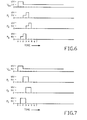
- Figure 6 is a timing diagram which shows the sequence of programming pulses required to program the interface 12' so that P 1 will be coupled to I 2 , P 2 coupled to I3 and P 3 coupled to I 1 .
- the duration of each of the pulses is arbitrary and can be made as short as desired, considering of course, the circuit response time.
- the programming pulses as shown in Figure 5 can be seen to have two levels, 5 and 10 volts. This two level type pulse is shown in Figure 5 to emphasize that certain functions must occur before others in order that the circuit operate properly.
- the first step in programming is to raise VCC from its normal 5 volt level to 10 volts (time 0). This initiates the programming sequence by erasing all previous programming. If one of the EEROMs in any column had been set, a high signal will appear on the DIS line for that column (through diode 23 or 23' of the associated coupler). A 10 volt signal on VCC in conjunction with a signal on the DIS line will turn the associated AND gate 32 on which will in turn apply a signal to the RST terminals of each coupler 14 in the column, erasing the EEROM that had been set (if it was in a coupler 14).
- a low signal from the EEROMs 22, 22' assures that AND gates 20, 20' and 24, 24' are off and therefore that the ENO outputs are low.
- the only couplers which are in condition to have their EEROMs set are couplers 13, all of which are associated with the I 1 bus.
- the priority sequence which is utilized in programming the presently preferred embodiment of the invention is to first couple I 1 to its associated P bus, followed by I 2 , I3 etc., in order, until all of the I inputs are coupled to the desired P input terminals.
- the enable interconnections (ENO and ENI) between the couplers assure that this sequence is followed.
- EEROM 22 of coupler 14-1-2 becomes set since there are then signals on the P 1 bus and on terminals ENI and LKT of the coupler.
- the LKT signal is present because there are no EEROMs in column 1 set.
- the absence of a set EEROM results in no DIS signal which in turn, because of inverter 33, results in LKT being high.
- AND gate 20 couples terminal P 1 to the I 2 bus.
- a DIS signal also appears on coupler 14-1-2 and LKT goes low on all couplers in column 1 assuring that no more E E ROMs in column 1 can be set.
- P 2 is raised to 5 volts and the same sequence of steps as outlined above sets EEROM 22 of coupler 14-2-3. It is not necessary to raise P 2 to 10 volts as it was in connection with programming the couplers for I 1 and I 2 . This is because the 10 volt level is used to enable the programming of the following I bus and since 1 3 is the last I bus in the example described there is no following I bus. For purposes of consistency, however, this pulse is shown having the same form as the others.
- Each of the I busses feeds into an AND gate 34.
- the purpose of the AND gates 34 is to avoid coupling a programming signal (from a P bus) to the system 11' while the programming sequence is under way. This is avoided by interrupting the signal flow along an I bus during the time that programming of that bus is in progress. Specifically, whenever the enable input or output of a Control Signal Coupler is high, the associated NOR gate 35 causes AND gate 34 to decouple the I bus from system 11'.
- the reprogramming would start at time zero by raising VCC to 10 volts as before, but at time 1, instead of initiating a programming pulse on P 3 , the first programming pulse would be applied to the P bus which is desired to be coupled to I 1 , namely P 1 . The next programming pulse would be on P 2 since it is intended that P 2 be coupled to I 2 . The last programming pulse would then be applied to P 3 .
Landscapes
- Engineering & Computer Science (AREA)
- General Engineering & Computer Science (AREA)
- Theoretical Computer Science (AREA)
- Computer Networks & Wireless Communication (AREA)
- Computer Hardware Design (AREA)
- Physics & Mathematics (AREA)
- General Physics & Mathematics (AREA)
- Logic Circuits (AREA)
- Circuits Of Receivers In General (AREA)
- Communication Control (AREA)
- Programmable Controllers (AREA)
Applications Claiming Priority (2)
| Application Number | Priority Date | Filing Date | Title |
|---|---|---|---|
| US06/745,580 US4644353A (en) | 1985-06-17 | 1985-06-17 | Programmable interface |
| US745580 | 2003-12-29 |
Publications (2)
| Publication Number | Publication Date |
|---|---|
| EP0206102A2 true EP0206102A2 (de) | 1986-12-30 |
| EP0206102A3 EP0206102A3 (de) | 1988-05-04 |
Family
ID=24997313
Family Applications (1)
| Application Number | Title | Priority Date | Filing Date |
|---|---|---|---|
| EP86107910A Withdrawn EP0206102A3 (de) | 1985-06-17 | 1986-06-10 | Programmierbare Schnittstelle |
Country Status (3)
| Country | Link |
|---|---|
| US (1) | US4644353A (de) |
| EP (1) | EP0206102A3 (de) |
| JP (1) | JPS61290517A (de) |
Cited By (3)
| Publication number | Priority date | Publication date | Assignee | Title |
|---|---|---|---|---|
| EP0361142A3 (de) * | 1988-09-29 | 1992-09-02 | Siemens Aktiengesellschaft | Universeller Standard-Bus |
| EP0573637A4 (de) * | 1991-12-26 | 1994-03-16 | Altera Corporation | |
| EP1043662A1 (de) * | 1999-04-08 | 2000-10-11 | Microchip Technology Inc. | Vorrichtung und Verfahren zum Rekonfigurieren der Stiftenzuweisung von einer oder mehreren Funktionsschaltungen in einem Mikrokontroller |
Families Citing this family (1)
| Publication number | Priority date | Publication date | Assignee | Title |
|---|---|---|---|---|
| JP4755050B2 (ja) * | 2006-08-18 | 2011-08-24 | 富士通株式会社 | データ処理装置、モード管理装置、及びモード管理方法 |
Family Cites Families (9)
| Publication number | Priority date | Publication date | Assignee | Title |
|---|---|---|---|---|
| NL6712617A (de) * | 1967-09-15 | 1969-03-18 | ||
| US3510850A (en) * | 1968-04-30 | 1970-05-05 | Gen Electric | Drive circuitry for negative resistance device matrix |
| US3872439A (en) * | 1973-02-09 | 1975-03-18 | Hassan Paddy Abdel Salam | Electronic switching circuit for bidirectional transfer |
| NL7503539A (nl) * | 1974-04-05 | 1975-10-07 | Cselt Centro Studi Lab Telecom | Logische keten voor het verdichten van digitale gegevens. |
| JPS5169908A (en) * | 1974-12-16 | 1976-06-17 | Hitachi Ltd | Tsuwaromono seigyohoshiki |
| US4289982A (en) * | 1979-06-28 | 1981-09-15 | Motorola, Inc. | Apparatus for programming a dynamic EPROM |
| US4490812A (en) * | 1982-09-30 | 1984-12-25 | Mostek Corporation | User reprogrammable programmed logic array |
| JPS605493A (ja) * | 1983-06-22 | 1985-01-12 | Toshiba Corp | 半導体記憶装置 |
| US4551814A (en) * | 1983-12-12 | 1985-11-05 | Aerojet-General Corporation | Functionally redundant logic network architectures |
-
1985
- 1985-06-17 US US06/745,580 patent/US4644353A/en not_active Expired - Lifetime
-
1986
- 1986-06-10 EP EP86107910A patent/EP0206102A3/de not_active Withdrawn
- 1986-06-16 JP JP61138437A patent/JPS61290517A/ja active Granted
Cited By (4)
| Publication number | Priority date | Publication date | Assignee | Title |
|---|---|---|---|---|
| EP0361142A3 (de) * | 1988-09-29 | 1992-09-02 | Siemens Aktiengesellschaft | Universeller Standard-Bus |
| EP0573637A4 (de) * | 1991-12-26 | 1994-03-16 | Altera Corporation | |
| US5517186A (en) * | 1991-12-26 | 1996-05-14 | Altera Corporation | EPROM-based crossbar switch with zero standby power |
| EP1043662A1 (de) * | 1999-04-08 | 2000-10-11 | Microchip Technology Inc. | Vorrichtung und Verfahren zum Rekonfigurieren der Stiftenzuweisung von einer oder mehreren Funktionsschaltungen in einem Mikrokontroller |
Also Published As
| Publication number | Publication date |
|---|---|
| JPS61290517A (ja) | 1986-12-20 |
| EP0206102A3 (de) | 1988-05-04 |
| JPH0517567B2 (de) | 1993-03-09 |
| US4644353A (en) | 1987-02-17 |
Similar Documents
| Publication | Publication Date | Title |
|---|---|---|
| EP0253530B1 (de) | Dynamisch rekonfigurierbare Feldlogik | |
| KR100187299B1 (ko) | 프로그램이 가능한 논리장치를 위한 입력 열 구동기 | |
| KR950015009B1 (ko) | 배치가능한 반도체 집적회로 | |
| US4940909A (en) | Configuration control circuit for programmable logic devices | |
| JP3507488B2 (ja) | システム内でのプログラミングのためのピンを多重化する方法及び構造 | |
| US5303181A (en) | Programmable chip enable logic function | |
| US5329179A (en) | Arrangement for parallel programming of in-system programmable IC logical devices | |
| US4527115A (en) | Configurable logic gate array | |
| US4799140A (en) | Majority vote sequencer | |
| EP0247809B1 (de) | Programmierbares logisches Gerät | |
| US4975641A (en) | Integrated circuit and method for testing the integrated circuit | |
| JPH0774621A (ja) | プログラム可能な集積論理装置 | |
| KR910005615B1 (ko) | 프로그래머블 순차코오드 인식회로 | |
| JPS6234293B2 (de) | ||
| US4930107A (en) | Method and apparatus for programming and verifying programmable elements in programmable devices | |
| US5982683A (en) | Enhanced method of testing semiconductor devices having nonvolatile elements | |
| US5453706A (en) | Field programmable gate array providing contention free configuration and reconfiguration | |
| DE10231956A1 (de) | Verfahren und Vorrichtung zur systeminternen Programmierung durch einen gemeinsamen Verbindungspunkt von programmierbaren logischen Bauelementen auf mehreren Schaltungsplatinen eines Systems | |
| KR100223623B1 (ko) | 비휘발성 기억셀용 테스트 회로 | |
| US4644353A (en) | Programmable interface | |
| US6334208B1 (en) | Method and apparatus for in-system programming with a status bit | |
| US5465055A (en) | RAM-logic tile for field programmable gate arrays | |
| EP0173357A1 (de) | Binärschaltung mit wählbarer Ausgangspolarität | |
| KR900003884A (ko) | 대규모 반도체 집적회로 장치 | |
| US5550842A (en) | EEPROM verification circuit with PMOS transistors |
Legal Events
| Date | Code | Title | Description |
|---|---|---|---|
| PUAI | Public reference made under article 153(3) epc to a published international application that has entered the european phase |
Free format text: ORIGINAL CODE: 0009012 |
|
| AK | Designated contracting states |
Kind code of ref document: A2 Designated state(s): DE FR GB |
|
| RIN1 | Information on inventor provided before grant (corrected) |
Inventor name: WEI, JAMES JUAN |
|
| PUAL | Search report despatched |
Free format text: ORIGINAL CODE: 0009013 |
|
| AK | Designated contracting states |
Kind code of ref document: A3 Designated state(s): DE FR GB |
|
| 17P | Request for examination filed |
Effective date: 19881022 |
|
| 17Q | First examination report despatched |
Effective date: 19890216 |
|
| STAA | Information on the status of an ep patent application or granted ep patent |
Free format text: STATUS: THE APPLICATION IS DEEMED TO BE WITHDRAWN |
|
| 18D | Application deemed to be withdrawn |
Effective date: 19901016 |
|
| RIN1 | Information on inventor provided before grant (corrected) |
Inventor name: WEI, JAMES JUAN |