EP0206136A2 - Procédé pour fabriquer un dispositif à semi-conducteur - Google Patents
Procédé pour fabriquer un dispositif à semi-conducteur Download PDFInfo
- Publication number
- EP0206136A2 EP0206136A2 EP86108001A EP86108001A EP0206136A2 EP 0206136 A2 EP0206136 A2 EP 0206136A2 EP 86108001 A EP86108001 A EP 86108001A EP 86108001 A EP86108001 A EP 86108001A EP 0206136 A2 EP0206136 A2 EP 0206136A2
- Authority
- EP
- European Patent Office
- Prior art keywords
- region
- semiconductor substrate
- forming
- oxide film
- type
- Prior art date
- Legal status (The legal status is an assumption and is not a legal conclusion. Google has not performed a legal analysis and makes no representation as to the accuracy of the status listed.)
- Granted
Links
Images


Classifications
-
- H—ELECTRICITY
- H10—SEMICONDUCTOR DEVICES; ELECTRIC SOLID-STATE DEVICES NOT OTHERWISE PROVIDED FOR
- H10D—INORGANIC ELECTRIC SEMICONDUCTOR DEVICES
- H10D18/00—Thyristors
- H10D18/01—Manufacture or treatment
-
- H—ELECTRICITY
- H10—SEMICONDUCTOR DEVICES; ELECTRIC SOLID-STATE DEVICES NOT OTHERWISE PROVIDED FOR
- H10D—INORGANIC ELECTRIC SEMICONDUCTOR DEVICES
- H10D18/00—Thyristors
- H10D18/60—Gate-turn-off devices
-
- H—ELECTRICITY
- H10—SEMICONDUCTOR DEVICES; ELECTRIC SOLID-STATE DEVICES NOT OTHERWISE PROVIDED FOR
- H10D—INORGANIC ELECTRIC SEMICONDUCTOR DEVICES
- H10D62/00—Semiconductor bodies, or regions thereof, of devices having potential barriers
- H10D62/10—Shapes, relative sizes or dispositions of the regions of the semiconductor bodies; Shapes of the semiconductor bodies
- H10D62/13—Semiconductor regions connected to electrodes carrying current to be rectified, amplified or switched, e.g. source or drain regions
- H10D62/141—Anode or cathode regions of thyristors; Collector or emitter regions of gated bipolar-mode devices, e.g. of IGBTs
- H10D62/142—Anode regions of thyristors or collector regions of gated bipolar-mode devices
Definitions
- This invention relates to a semiconductor device manufacturing method and more particularly to a method for manufacturing an anode-emitter shorting type gate turn-off thyristors (AN-GTO).
- AN-GTO an anode-emitter shorting type gate turn-off thyristors
- Fig. 1 shows a top view of an AN-GTO.
- Fig. 2 shows a cross sectional view taken on line I - I of Fig. 1.
- an n--type semiconductor substrate 12 is prepared.
- This AN-GTO includes p-type region 14 formed in the upper surface of substrate 12, and p-type region 16 formed in the bottom surface of substrate 12.
- the p-type region 16 is used as the anode-emitter of the AN-GTO.
- the cathode emitter of the AN-GTO is composed of radially distributed n +- type regions 18, as shown in the Fig. 1.
- n +- type regions 18 are obtained by patterning an n-type region (not shown) which is formed on the entire surface of p-type region 16.
- the AN-GTO includes n +- type regions 20 in the bottom surface of the n-type substrate. The regions 20 serves as shorting sections.
- the n +- type regions 20, as shown in Fig. 2, are located under the bottom of n +- type regions 18.
- Anode electrode 22 of the AN-G T O is formed in contact with n +- type regions 20 and p-type region 16.
- Cathode electrodes 24 are formed in contact with n +- type regions 18.
- Gate electrodes 25 are formed in contact with p-type region 14.
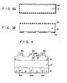
- Figs. 3A and 3 B shows manufacturing steps for the AN-GTO.
- oxide film 26 is formed on the entire surface of n--type substrate 12.
- Oxide film 26 is patterned on the bottom surface of substrate 12, as shown in Fig. 3B.
- the n +- type regions 20A through 20C are formed, following the patterning process, by diffusing impurity into the substrate 12 with the mask of the remaining oxide film 26.
- oxide film 26 cannot fulfill its role as a diffusion protecting film, in the forming process of n +- type regions 20. This is because the impurities will pass through the pin-holes and diffuse into substrate 12, thus forming unnecessary n +- type regions.
- the unnecessary n +- type regions will be thermally diffused to grow to the size of n +- type regions 28A and 28B, as shown in Fig. 4.
- n f- type regions 28A and 28B will deteriorate the forward blocking voltage characteristic of the AN-GTO.
- an object of the present invention is to provide a method of manufacturing a semiconductor device with excellent forward blocking voltage characteristic at a high production yield.
- a semiconductor device manufacturing method comprising a first step of preparing a semiconductor substrate of a first conductivity type having first and second surfaces, a second step of forming an oxide film pattern on the first surface of the semiconductor substrate, a third step of forming a first region of the first conductivity type in the first surface of the semiconductor substrate by using a mask of the oxide film pattern, with a higher impurity concentration than the semiconductor substrate, and a fourth step of forming a second region of a second conductivity type in the first surface of the semiconductor substrate with a depth shallower than the first region, after removal of the oxide film pattern, and forming a third region of the second conductivity type in the second surface of the semiconductor substrate, characterized by further comprising a fifth step of removing a part of the semiconductor substrate on the second surface side by a predetermined thickness, before formation of the third region (38B).
- FIGs. 5A through 5J illustrate steps for manufacturing an anode shorting type gate turn-off thyristor (AN-GTO).
- AN-GTO an anode shorting type gate turn-off thyristor
- a first step n--type substrate 30 containing n-type impurity at a low concentration is prepared.
- Oxide film 32 is formed on the substrate 30 with a uniform thickness and covers the entire surface of substrate 30, as shown in F ig. 5A.
- resist pattern 34 is formed on oxide film 32 over the bottom surface of substrate 30, as shown in Fig. 5B.
- Oxide film 26 is subjected to an etching process with a use of resist pattern 34 as a mask. In this process, oxide film 26 is completely removed from the upper surface of substrate 30, and partially removed from the bottom surface, oxide film pattern 34 being left on the bottom surface of substrate 30, as shown in F ig. 5C.
- n-type impurity such as phosphorus
- oxide film pattern 34 is doped in the exposed surface of semiconductor substrate 30, using oxide film pattern 34 as a mask.
- nt-type diffusion regions 36A and 36B with high impurity concentration are formed in the bottom and top surfaces of substrate 30.
- substrate 30 is subjected to the lapping process.
- the lapping process the upper surface area of substrate 30 is lapped away by a predetermined thickness D.
- the thickness D is so selected to be greater than the depth of diffusion region 36B, as shown in Fig. 5E, in order to completely remove diffusion region 36 B from semiconductor substrate 30.
- the step of Fig. 5E may includes an etching process or etching-lapping process instead of the lapping process.
- the p-type impurity such as galium is doped into the substrate 30.
- p-type diffusion regions 38A and 38B are respectively formed in the bottom and top surfaces of substrate 30, as shown in Fig. 5F.
- the amount of doping impurity and the doping time are selected to a value at which the conductivity type of the diffusion regions 36A is not inverted.
- regions 36A grow as shown in Fig. 5F, due to the thermal diffusion of impurities.
- Diffusion region 38A is formed shallower than diffusion regions 36A as grown in order to use the regions 36A as the anode shorting regions.
- n-type impurity is doped in the top surface of the semiconductor substrate to form n +- type diffusion region 40 with a uniform thickness, as shown in Fig. 5G.
- resist pattern 42 is applied to the top of diffusion region 40, and selectively masks region 40 corresponding to the positions of diffusion regions 36A. After this, an etching process is performed, using the resist pattern 42 as a mask. As shown in F ig. 5I, portions of diffusion regions 40 and 38 B are selectively removed through the process. The remaining diffusion regions 40A through 40D are used as the cathode-emitter of the AN-GTO.
- cathode electrodes 44 are formed in ohmic contact with diffusion regions 40A through 40D
- gate electrodes 48 are formed in contact with diffusion region 38B
- anode electrodes 46 are formed in ohmic contact with diffusion regions 38A and 36A.
- an unnecessary diffusion region 36B is formed by the process of Fig. 5D, but this region has been completely removed before diffusion region 38 B is formed. Even if heat is applied to the semiconductor structure in the steps succeeding to the step of Fig. 5F, a shorting portion will not be formed on the cathode side of the AN-GTO. Also, even in case diffusion region 36B is not completely removed, as long as region 36B grows in diffusion region 38B, the deterioration of a forward blocking electrical characteristic of the AN-GTO will be prevented.
- oxide film 32 it is not necessary to leave oxide film 32 on the top surface of semiconductor substrate 30 in the etching process of the oxide film 32.
- a resist film in order for oxide film 32 to perform its role as a diffusion protective film on the top surface of semiconductor substrate 30, a resist film must be applied beforehand to the top of the protective film, so that it will not be removed by the etching process.
Landscapes
- Thyristors (AREA)
Applications Claiming Priority (2)
| Application Number | Priority Date | Filing Date | Title |
|---|---|---|---|
| JP60127502A JPH0715991B2 (ja) | 1985-06-12 | 1985-06-12 | 半導体装置の製造方法 |
| JP127502/85 | 1985-06-12 |
Publications (3)
| Publication Number | Publication Date |
|---|---|
| EP0206136A2 true EP0206136A2 (fr) | 1986-12-30 |
| EP0206136A3 EP0206136A3 (en) | 1988-09-28 |
| EP0206136B1 EP0206136B1 (fr) | 1991-07-03 |
Family
ID=14961560
Family Applications (1)
| Application Number | Title | Priority Date | Filing Date |
|---|---|---|---|
| EP86108001A Expired EP0206136B1 (fr) | 1985-06-12 | 1986-06-12 | Procédé pour fabriquer un dispositif à semi-conducteur |
Country Status (3)
| Country | Link |
|---|---|
| EP (1) | EP0206136B1 (fr) |
| JP (1) | JPH0715991B2 (fr) |
| DE (1) | DE3680036D1 (fr) |
Cited By (6)
| Publication number | Priority date | Publication date | Assignee | Title |
|---|---|---|---|---|
| EP0345435A3 (en) * | 1988-04-08 | 1990-04-25 | Kabushiki Kaisha Toshiba | Semiconductor device with a high breakdown voltage and method for its manufacture |
| EP0366916A3 (fr) * | 1988-10-04 | 1991-08-28 | Kabushiki Kaisha Toshiba | Dispositif semi-conducteur à anode court-circuitée et méthodes de fabrication |
| EP0435021A3 (en) * | 1989-12-19 | 1992-04-15 | Eupec Europaeische Gesellschaft Fuer Leistungshalbleiter Mbh & Co. Kg | Method for manufacturing anode side short circuits in thyristors |
| WO1993001620A1 (fr) * | 1991-07-01 | 1993-01-21 | Asea Brown Boveri Ab | Thyristor blocable et procede de fabrication |
| US5223442A (en) * | 1988-04-08 | 1993-06-29 | Kabushiki Kaisha Toshiba | Method of making a semiconductor device of a high withstand voltage |
| US5248622A (en) * | 1988-10-04 | 1993-09-28 | Kabushiki Kashiba Toshiba | Finely controlled semiconductor device and method of manufacturing the same |
Family Cites Families (3)
| Publication number | Priority date | Publication date | Assignee | Title |
|---|---|---|---|---|
| JPS5336180A (en) * | 1976-09-16 | 1978-04-04 | Hitachi Ltd | Production of semiconductor device |
| JPS56112753A (en) * | 1980-02-13 | 1981-09-05 | Hitachi Ltd | Gate turn-off thyristor |
| JPS59205566A (ja) * | 1983-05-09 | 1984-11-21 | 株式会社東芝 | 冷蔵庫 |
-
1985
- 1985-06-12 JP JP60127502A patent/JPH0715991B2/ja not_active Expired - Lifetime
-
1986
- 1986-06-12 DE DE8686108001T patent/DE3680036D1/de not_active Expired - Lifetime
- 1986-06-12 EP EP86108001A patent/EP0206136B1/fr not_active Expired
Cited By (8)
| Publication number | Priority date | Publication date | Assignee | Title |
|---|---|---|---|---|
| EP0345435A3 (en) * | 1988-04-08 | 1990-04-25 | Kabushiki Kaisha Toshiba | Semiconductor device with a high breakdown voltage and method for its manufacture |
| US5156981A (en) * | 1988-04-08 | 1992-10-20 | Kabushiki Kaisha Toshiba | Method of making a semiconductor device of a high withstand voltage |
| US5223442A (en) * | 1988-04-08 | 1993-06-29 | Kabushiki Kaisha Toshiba | Method of making a semiconductor device of a high withstand voltage |
| EP0366916A3 (fr) * | 1988-10-04 | 1991-08-28 | Kabushiki Kaisha Toshiba | Dispositif semi-conducteur à anode court-circuitée et méthodes de fabrication |
| US5148254A (en) * | 1988-10-04 | 1992-09-15 | Kabushiki Kaisha Toshiba | Finely controlled semiconductor device |
| US5248622A (en) * | 1988-10-04 | 1993-09-28 | Kabushiki Kashiba Toshiba | Finely controlled semiconductor device and method of manufacturing the same |
| EP0435021A3 (en) * | 1989-12-19 | 1992-04-15 | Eupec Europaeische Gesellschaft Fuer Leistungshalbleiter Mbh & Co. Kg | Method for manufacturing anode side short circuits in thyristors |
| WO1993001620A1 (fr) * | 1991-07-01 | 1993-01-21 | Asea Brown Boveri Ab | Thyristor blocable et procede de fabrication |
Also Published As
| Publication number | Publication date |
|---|---|
| DE3680036D1 (de) | 1991-08-08 |
| JPS61285766A (ja) | 1986-12-16 |
| EP0206136A3 (en) | 1988-09-28 |
| EP0206136B1 (fr) | 1991-07-03 |
| JPH0715991B2 (ja) | 1995-02-22 |
Similar Documents
| Publication | Publication Date | Title |
|---|---|---|
| KR960000387B1 (ko) | 반도체 장치 제조방법 | |
| US4498227A (en) | Wafer fabrication by implanting through protective layer | |
| US4499657A (en) | Method of making a semiconductor device having protected edges | |
| EP0345435B1 (fr) | Dispositif semi-conducteur à haute tension de claquage et procédé pour sa fabrication | |
| US3717514A (en) | Single crystal silicon contact for integrated circuits and method for making same | |
| JPS6140146B2 (fr) | ||
| KR0171128B1 (ko) | 수직형 바이폴라 트랜지스터 | |
| EP0685891B1 (fr) | Diode semi-conductrice intégrée | |
| US4473941A (en) | Method of fabricating zener diodes | |
| EP0194832A2 (fr) | Construction d'un transistor bipolaire | |
| GB2082386A (en) | Zener diodes and their manufacture | |
| EP0206136B1 (fr) | Procédé pour fabriquer un dispositif à semi-conducteur | |
| KR960019776A (ko) | 반도체장치 및 그 제조방법 | |
| JPH0738102A (ja) | 高耐圧半導体装置の製造方法 | |
| JP2573201B2 (ja) | 半導体素子の拡散層形成方法 | |
| US4304043A (en) | Process for preparing semiconductor device _by forming reinforcing regions to facilitate separation of pellets | |
| EP0288681A1 (fr) | Transistor bipolaire à hétérojonction | |
| JPS6097659A (ja) | 半導体集積回路 | |
| US4713355A (en) | Bipolar transistor construction | |
| US3825451A (en) | Method for fabricating polycrystalline structures for integrated circuits | |
| CA1041221A (fr) | Jonction pn a equilibre thermique | |
| GB1593937A (en) | I2l integrated circuitry | |
| EP0194199B1 (fr) | Thyristor à induction statique à double porte et son procédé de fabrication | |
| CA1205577A (fr) | Dispositif semiconducteur | |
| US5143859A (en) | Method of manufacturing a static induction type switching device |
Legal Events
| Date | Code | Title | Description |
|---|---|---|---|
| PUAI | Public reference made under article 153(3) epc to a published international application that has entered the european phase |
Free format text: ORIGINAL CODE: 0009012 |
|
| 17P | Request for examination filed |
Effective date: 19860612 |
|
| AK | Designated contracting states |
Kind code of ref document: A2 Designated state(s): CH DE FR GB LI |
|
| PUAL | Search report despatched |
Free format text: ORIGINAL CODE: 0009013 |
|
| AK | Designated contracting states |
Kind code of ref document: A3 Designated state(s): CH DE FR GB LI |
|
| 17Q | First examination report despatched |
Effective date: 19900313 |
|
| GRAA | (expected) grant |
Free format text: ORIGINAL CODE: 0009210 |
|
| AK | Designated contracting states |
Kind code of ref document: B1 Designated state(s): CH DE FR GB LI |
|
| REF | Corresponds to: |
Ref document number: 3680036 Country of ref document: DE Date of ref document: 19910808 |
|
| ET | Fr: translation filed | ||
| PLBE | No opposition filed within time limit |
Free format text: ORIGINAL CODE: 0009261 |
|
| STAA | Information on the status of an ep patent application or granted ep patent |
Free format text: STATUS: NO OPPOSITION FILED WITHIN TIME LIMIT |
|
| 26N | No opposition filed | ||
| PGFP | Annual fee paid to national office [announced via postgrant information from national office to epo] |
Ref country code: GB Payment date: 19970603 Year of fee payment: 12 |
|
| PGFP | Annual fee paid to national office [announced via postgrant information from national office to epo] |
Ref country code: FR Payment date: 19970610 Year of fee payment: 12 |
|
| PGFP | Annual fee paid to national office [announced via postgrant information from national office to epo] |
Ref country code: DE Payment date: 19970620 Year of fee payment: 12 |
|
| PG25 | Lapsed in a contracting state [announced via postgrant information from national office to epo] |
Ref country code: GB Free format text: LAPSE BECAUSE OF NON-PAYMENT OF DUE FEES Effective date: 19980612 |
|
| GBPC | Gb: european patent ceased through non-payment of renewal fee |
Effective date: 19980612 |
|
| PG25 | Lapsed in a contracting state [announced via postgrant information from national office to epo] |
Ref country code: FR Free format text: LAPSE BECAUSE OF NON-PAYMENT OF DUE FEES Effective date: 19990226 |
|
| PG25 | Lapsed in a contracting state [announced via postgrant information from national office to epo] |
Ref country code: DE Free format text: LAPSE BECAUSE OF NON-PAYMENT OF DUE FEES Effective date: 19990401 |
|
| REG | Reference to a national code |
Ref country code: FR Ref legal event code: ST |
|
| PGFP | Annual fee paid to national office [announced via postgrant information from national office to epo] |
Ref country code: CH Payment date: 20050615 Year of fee payment: 20 |
|
| REG | Reference to a national code |
Ref country code: CH Ref legal event code: PL |