EP0206409B1 - Système de transmission numérique d'ordre supérieur comprenant un multiplexeur et un démultiplexeur - Google Patents
Système de transmission numérique d'ordre supérieur comprenant un multiplexeur et un démultiplexeur Download PDFInfo
- Publication number
- EP0206409B1 EP0206409B1 EP19860201034 EP86201034A EP0206409B1 EP 0206409 B1 EP0206409 B1 EP 0206409B1 EP 19860201034 EP19860201034 EP 19860201034 EP 86201034 A EP86201034 A EP 86201034A EP 0206409 B1 EP0206409 B1 EP 0206409B1
- Authority
- EP
- European Patent Office
- Prior art keywords
- arrangement
- demultiplexer
- digital signal
- block
- multiplexer
- Prior art date
- Legal status (The legal status is an assumption and is not a legal conclusion. Google has not performed a legal analysis and makes no representation as to the accuracy of the status listed.)
- Expired
Links
- 230000005540 biological transmission Effects 0.000 title claims description 27
- 239000002131 composite material Substances 0.000 claims description 9
- 230000001360 synchronised effect Effects 0.000 claims description 6
- 238000010586 diagram Methods 0.000 description 11
- 238000000034 method Methods 0.000 description 5
- 230000008569 process Effects 0.000 description 3
- 238000001514 detection method Methods 0.000 description 2
- 238000012545 processing Methods 0.000 description 2
- 230000004044 response Effects 0.000 description 2
- 238000013519 translation Methods 0.000 description 2
- 230000000903 blocking effect Effects 0.000 description 1
- 230000008878 coupling Effects 0.000 description 1
- 238000010168 coupling process Methods 0.000 description 1
- 238000005859 coupling reaction Methods 0.000 description 1
- 238000013461 design Methods 0.000 description 1
- 230000006870 function Effects 0.000 description 1
- 230000010354 integration Effects 0.000 description 1
- 239000011159 matrix material Substances 0.000 description 1
- 238000012544 monitoring process Methods 0.000 description 1
- 230000003287 optical effect Effects 0.000 description 1
- 239000013307 optical fiber Substances 0.000 description 1
- 230000002035 prolonged effect Effects 0.000 description 1
- 230000001172 regenerating effect Effects 0.000 description 1
- 238000012552 review Methods 0.000 description 1
- 230000001629 suppression Effects 0.000 description 1
Images

Classifications
-
- H—ELECTRICITY
- H04—ELECTRIC COMMUNICATION TECHNIQUE
- H04J—MULTIPLEX COMMUNICATION
- H04J3/00—Time-division multiplex systems
- H04J3/02—Details
- H04J3/06—Synchronising arrangements
- H04J3/0602—Systems characterised by the synchronising information used
- H04J3/0605—Special codes used as synchronising signal
-
- H—ELECTRICITY
- H04—ELECTRIC COMMUNICATION TECHNIQUE
- H04J—MULTIPLEX COMMUNICATION
- H04J3/00—Time-division multiplex systems
- H04J3/02—Details
- H04J3/04—Distributors combined with modulators or demodulators
- H04J3/047—Distributors with transistors or integrated circuits
Definitions
- the invention relates to a higher order digital transmission system including a digital multiplexer having N parallel inputs, and a digital demultiplexer having N parallel outputs for transmitting mutually synchronized digital signal streams through a common digital path between said multiplexer and demultiplexer, where N ⁇ 2 and the multiplexer being arranged for cyclically and symbol-sequential interleaving the digital signal streams to form a composite digital signal stream, the transmission system further including at least one block encoding arrangement and at least one block decoding arrangement, and a phase comparator arrangement, the digital signal streams being entered synchronously under the control of a common clock signal into the encoding arrangement and being applied to the N parallel inputs of the multiplexer via the block encoding arrangement, the parallel ouputs of the demultiplexer being connected to the inputs of the block encoding arrangement, the signals applied to the parallel outputs of the demultiplexer being entered into the block decoding arrangement under the control of the clock signal recovered from the composite digital signal, the outputs of the block decoding arrangement being
- N incoming signal streams are combined to form one outgoing signal stream, whilst the opposite operation occurs in the demultiplexer.
- Multiplexing the incoming signal streams is effected by means of interleaving, which implies that a bit from a binary signal stream 1 is followed by a bit from a binary signal stream 2 etc.
- the resultant outgoing signal stream has a digital rate which is higher than or equal to N times the digital rate of the N incoming signal streams. This is caused by the fact that the outgoing signal stream requires its own frame word and a few service bits, which are added to the outgoing signal stream. Provisions are also taken to compensate for frequency differences between the tributary signal streams and the multiplex clock.
- This digital path may, for example, be constituted by symmetrical or coaxial cables, optical fibres or the air.
- One of the objects usually is the suppression of the direct current component, which permits of the use of alternating current couplings in the transmission system, and direct current supply of the regenerators from the transmission system via the transmission cable being possible.
- Another object often is to increase the pulse density of the digital signal to be conveyed, or to ensure a minimum pulse density such that recovering a clock signal, required in regenerative circuits, is possible.
- a series/parallel converter which divides the bit stream applied to its input in consecutive blocks of a predetermined number of bits n is provided at the input of the encoding arrangement.
- a block of n bits is thereafter converted with the aid of the translation code matrix into a new block of m symbols in accordance with a specific instruction.
- Blocks of m symbols are reconverted at the output of the encoding arrangement with the aid of a parallel/series converter into a bit stream which is conveyed to the receiver portion of the digital transmission system via the digital path (cable, optical fibre).
- the bit stream applied there is subjected to a reverse process with the aid of the decoding arrangement.
- Examples of an encoding arrangement and a de-coding arrangement are described in, for example, Proceedings 17th International Scientific Congress on Electronics, Rome, 16-18 March 1970, pages 275-283.
- a higher order digital multiplex system of the above-defined type is disclosed in, for example, C.C.I.T.T. Recommendation G922.
- the frame structure of a multiplex system having 4 tributary signal streams of 140 Mbit/s each is described.
- a frame has a length of 2688 bits and comprises: a 12-bit frame synchronizing word; 4 service bits; 4 5-bit justification control words, one for each tributary signal stream; 4 justifiable bits, one for each tributary signal stream and 2648 time slots for the information from the four tributary signal streams.
- the block encoding arrangement is arranged subsequent to the multiplexer and the block decoding arrangement precedes the demultiplexer.
- the digital signal streams are, after these signal streams are synchronized by forming out of each signal stream a number of consecutive frames having a predetermined structure, applied in parallel to the 6 inputs of a 6B/8B block encoding arrangment and each set of 6 parallel inputs bits is converted into 8 parallel output bits, which in parallel are applied to the 8 inputs of the multiplexer.
- the composite digital signal stream first is applied to the 8 inputs of an 8B/6B block decoding arrangement, at the 6 outputs of which the orignally transmitted digital signal streams are available again.
- the phase comparator arrangement compares the frame synchronization characteristics, which are present in the received composite digital signal stream, with each other and controls the read clock of the multiplexer to obtain phase synchronization in the output signals of the decoding arrangment.
- the system according to this publication does not have the problem that the block encoding arrangements have to operate at the full line rate.
- this known system has the disadvantage that at the input side the digital signal streams have to be converted into consecutive frames having a predetermined structure, which requires a relatively complex synchronizing circuit for each of the input signals, while to obtain the required phase synchronization at the receiver end also a relatively complex circuit comprising a frame pattern detection circuit, a frame synchronizing circuit and a local frame generator are required, which circuits all have to operate at the full line rate.
- a further disadvantage of obtaining phase synchronization by comparing the phases of the consecutive frames is that it can take quite a long time before the correct phase is obtained.
- the invention has for its object to provide a higher order digital transmission system which solves also the problems that are still present in the system according to EP-A-0088432.
- the invention therefor provides a digital transmission system of the above mentioned kind characterized in that N mutually synchronized digital signal streams, are applied to the N parallel inputs of the multiplexer via N block encoding arrangements, in that the digital signal streams, in the respective block encoding arrangements, are provided with a word synchronization characteristic, that the N parallel outputs of the demultiplexer are entered into N block decoding arrangements and in that the outputs of the N block encoding arrangement are coupled to the input of the phase comparator, which is arranged to compare the word synchronizing characteristcs of the digital signal streams at the respective outputs of the block decoding arrangements.
- I is the transmitter portion of the system and II the receiver portion of the system.
- the transmitter portion I comprises the block encoding arrangements 1, 2, 3 and 4, the multiplexer 6, the divider 5 and the multipliers 7 and 9.
- the receiver portion II comprises the block decoding arrangements 12, 13, 14 and 15, the demultiplexer 11, the phase comparator 16, the divider 19 and the clock regenerator 17.
- the write clock inputs of the block encoding arrangements 1 to 4 are together connected to the clock input 8 of the transmitter portion I of the transmission system via the line 70.
- the clock input 8 is connected via a divide-by-5-divider and the line 71 to the clock inputs of the block encoding arrangements 1 to 4, which from the four digital signal streams A to D form 5-bit blocks, and also to the input of a multiply-by-6 multiplier 9.
- the output of the multiply-by-6 multiplier 9 is connected via the line 72 to the write clock inputs of the multiplexer 6 and also via a multiply-by-4 multiplier to the read clock outputs of the multiplexer 6.
- Each of the signal outputs 60 to 63 of the block encoding arrangements is connected to a signal input of the multiplexer 6.
- the signal output 65 of the multiplexer 6 is connected via a digital path 10 to the input 66 of the receiver portion II of the transmission system.
- the input 66 is connected to the signal input of the demultiplexer 11 and also to the input of the clock regenerator 17.
- the output of the clock regenerator 17 is connected to the clock input of the demultiplexer 11 and also to the input of a divide-by-4 divider 19.
- the output of the divider 19 is connected to the write clock inputs of the block decoding arrangements 12 to 15.
- the original digital signal streams A to D are again available at the outputs 44 to 47 of the block decoding arrangements 12.
- the outputs 40 to 43 of the block decoding arrangements 12 to 15 are each connected to an input of the phase comparator 16.
- These digital streams are entered synchronously into the 5B/6B block encoding arrangements 1 to 4 with the aid of the 140 MHz clock signal present on the line 70.
- the 140 Mbit/s signal streams are divided by means of the 28 MHz clock signal present on the line 71 into blocks each having a length of 5 symbols.
- the 5-bit blocks are thereafter translated in the block encoding arrangements into blocks of 6 symbols.
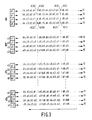
- the 6B words are each provided with a word synchronizing characteristic. Since the four parallel 5B/6B block encoding arrangements 1 to 4 are controlled by the same 28 MHz clock signal and the block encoding arrangements 1 to 4 are identical, the 6B words will appear with the same phases at the outputs 60 to 63 of the block encoding arrangements. This is shown schematically in the time-sequence diagram of Figure 2.
- the word synchronizing characteristics K(1) ... K(4) shown symbolically by means of upright lines arrive at the same instant at the outputs 60 ... 63 of the block encoding arrangements. Consequently, the mutual difference between the synchronizing characteristics is equal to 0 degrees.
- the composite digital signal is applied to the input 66 of the receiver sections II of the digital transmission system via the digital path 10.
- the clock regenerator 17 the clock signal which is used for further signal processing in the receiver portion II of the transmission system is recovered from the composite digital signal.
- the recovered 672 MHz clock signal is applied to the clock input of the multiplexer 11 and via a divider 19 to the clock inputs of the block decoding arrangements 12 to 15.
- the synchronizing characteristics K(1) and K(10) have a time lead relative to the other synchronising characteristics K(2) to K(4) and K(20) to K(40), respectively.
- the synchronizing characteristics K(1) and K(2) lead the synchronizing characteristics K(3) and K(4).
- the synchronising characteristics K(10) and K(20) likewise have a time lead relative to the characteristics K(30) and K(40).
- the synchronizing characteristic K(4) has a time lag relative to the other characteristics K(1) to K(3).
- the characteristic K(40) likewise lags the other characteristics K(10) to K(30).
- phase positions as shown in the Figures 3b to 3d are detected by means of the phase comparator arrangement 16, whereafter a control signal is applied to the divide-by-4 divider 15 for establishing synchronization between the multiplexer 6 and the demultiplexer 11.
- a control signal is applied to the divide-by-4 divider 15 for establishing synchronization between the multiplexer 6 and the demultiplexer 11.
- the phase comparator 16 detects a phase position as shown in Figure 3a, the original digital signal streams A, B, C and D are then again available in the appropriate sequence at the outputs 44 to 47) of the block decoding arrangements 12 to 15 and no control voltage is applied to the divide-by-4 divider 19.
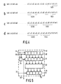
- the divide-by-4 divider 19 When the phase comparator 16 detects a phase position as shown in Figure 3b, the divide-by-4 divider 19 will operate once only as a divide-by-3 divider with the aid of the control signal produced by the phase comparator 16. This is shown in greater detail in Figure 4b.
- S(2) denotes the content of the demultiplexer 11 at the instant at which it is read in parallel. If now, in response to the control signal produced by the phase comparator 16, the divide-by-4 divider produces a write pulse once after three clock pulses which correspond to the symbols d2,c2,b2, the content of the demultiplexer 11 will be equal to S(20) after the next four clock pulses.
- the symbols a3, b3, c3 and d3 are now stored in the appropriate memory locations at the instant at which they are read in parallel, see Figure 3b.
- the demultiplexer 11 is now in synchronism with the multiplexer 6.
- the original digital signal streams A, B, C and D are then agains available in the appropriate sequence at the outputs 44 to 47 of the block decoding arrangements 12 to 15.
- the divide-by-4 divider 19 When the phase comparator detects a phase position as shown in Figure 3c, the divide-by-4 divider 19 will operate once as a divide-by-2 divider with the aid of the control signal produced by the phase comparator 16. This is shown in greater detail in Figure 4c.
- S(3) denotes the content of the demultiplexer 11 at the instant at which it is read in parallel. If now, with the aid of the control signal produced by the phase comparator 16 the divide-by-4 divider produces a write pulse once after two clock pulses which correspond to the symbols d2 and c2, the content of the demultiplexer 11 will be equal to S(30) after the next four clock pulses.
- the word synchronization in the block decoding arrangement is temporarily lost.
- the word synchronization is not restored until the symbols a to d, reference 6, have passed the input of the demultiplexer 11.
- the block coding arrangements 1 to 4 and the block decoding arrangements 12 to 15 are operated at an N times lower symbol rate it is possible to integrate said arrangements, in spite of the high line symbol rate of the transmission system.
- the described multiplexing method renders it possible to have all the signal processing operations, such as scrambling, justifying, line-coding, error-monitoring and word synchronization effected at an N times lower symbol rate.
- the multiplexer 6 and the demultiplexer 11 can be realized with the aid of a simple parallel/series converter and a simple series/parallel converter. It is also not necessary to add frame words and prolonged frame synchronization techniques.
- Figure 5 shows an embodiment of a block decoding arrangement. It comprises an input shift register 30, a buffer 31, a decoder unit 32, an output shift register 33 and a word synchronizer 34. With the aid of the 168 MHz clock signal present at the clock input 36 a word having 6 binary symbols is written into the series register 30 via the input 35; see, for example, Figure 3a the word a1...a6.
- the word synchronizer 34 produces, after detection of the synchronization characteristic K(40), a pulse in response to which the content of the series register 30 is transferred to the buffer 31. Said word synchronizing characteristic is also applied to an input of the phase comparator 16 via the line 40.
- the word having 6 binary symbols is converted into a word having 5 binary symbols which is applied in parallel to the output register 33.
- This output register is read with the aid of the 140 MHz clock signal present at the clock input 37.
- the original digital signal stream is available again at the output 44.
Landscapes
- Engineering & Computer Science (AREA)
- Computer Networks & Wireless Communication (AREA)
- Signal Processing (AREA)
- Microelectronics & Electronic Packaging (AREA)
- Synchronisation In Digital Transmission Systems (AREA)
- Time-Division Multiplex Systems (AREA)
- Dc Digital Transmission (AREA)
Claims (1)
- Système de transmission numérique d'ordre supérieur comprenant un multiplexeur numérique (6) comportant N entrées parallèles et un démultiplexeur numérique (11) comprenant N sorties parallèles pour transmettre des trains de signaux numériques mutuellement synchronisés (A-D) par un trajet numérique commun (16) entre le multiplexeur et le démultiplexeur, où N ≧ 2 et le multiplexeur est conçu pour imbriquer les trains de signaux numériques cycliquement et séquentiellement pour les symboles afin de former un train de signaux numériques composite, le système de transmission comprenant, en outre, au moins un dispositif de codage en blocs (1-4) et au moins un dispositif de décodage en blocs (12-18) et un dispositif comparateur de phase (16), les trains de signaux numériques étant introduits de manière synchrone, sous la commande d'un signal d'horloge commun, dans le dispositif de codage et étant appliqués aux N entrées parallèles du multiplexeur par l'intermédiaire du dispositif de codage en blocs, les sorties parallèles du démultiplexeur étant connectées aux entrées du dispositif de codage en blocs, les signaux des sorties parallèles du démultiplexeur étant introduits dans le dispositif de décodage en blocs sous la commande du signal d'horloge récupéré du signal numérique composite, les sorties du dispositif de décodage en blocs étant connectées chacune à une sortie de signal (44-47) du système de transmission et les caractéristiques de synchronisation des trains de signaux numériques étant comparées l'une à l'autre dans le dispositif comparateur de phase, après quoi, en fonction des différences de phase mesurées entre les caractéristiques de synchronisation, la phase de l'horloge de lecture est réglée de telle façon que par la suite les dispositifs de décodage en blocs affichent les caractéristiques de synchronisation avec les différences de phase mutuelles produites à l'extrémité d'émetteur, caractérisé en ce que N trains de signaux numériques mutuellement synchronisés sont appliqués aux N entrées parallèles du multiplexeur par l'intermédiaire de N dispositifs de codage en blocs, en ce que les trains de signaux numériques, dans les dispositifs de codage en blocs respectifs, sont pourvus d'une caractéristique de synchronisation de mot, que les N sorties parallèles du démultiplexeur sont introduites dans N dispositifs de décodage en blocs et en ce que les sorties des N dispositifs de décodage en blocs sont couplées à l'entrée du comparateur de phase qui est prévu pour comparer les caractéristiques de synchronisation de mot des trains de signaux numériques aux sorties respectives des dispositifs de décodage en blocs.
Applications Claiming Priority (2)
| Application Number | Priority Date | Filing Date | Title |
|---|---|---|---|
| NL8501738A NL8501738A (nl) | 1985-06-17 | 1985-06-17 | Hogere orde digitaal transmissiesysteem voorzien van een multiplexer en een demultiplexer. |
| NL8501738 | 1985-06-17 |
Publications (2)
| Publication Number | Publication Date |
|---|---|
| EP0206409A1 EP0206409A1 (fr) | 1986-12-30 |
| EP0206409B1 true EP0206409B1 (fr) | 1991-12-18 |
Family
ID=19846152
Family Applications (1)
| Application Number | Title | Priority Date | Filing Date |
|---|---|---|---|
| EP19860201034 Expired EP0206409B1 (fr) | 1985-06-17 | 1986-06-16 | Système de transmission numérique d'ordre supérieur comprenant un multiplexeur et un démultiplexeur |
Country Status (6)
| Country | Link |
|---|---|
| EP (1) | EP0206409B1 (fr) |
| JP (1) | JPH0712159B2 (fr) |
| AU (1) | AU596973B2 (fr) |
| CA (1) | CA1291832C (fr) |
| DE (1) | DE3682957D1 (fr) |
| NL (1) | NL8501738A (fr) |
Families Citing this family (6)
| Publication number | Priority date | Publication date | Assignee | Title |
|---|---|---|---|---|
| WO1988001815A1 (fr) * | 1986-08-30 | 1988-03-10 | Fujitsu Limited | Dispositif diviseur multiplex dans un systeme de multiplexage synchrone |
| JPS63236432A (ja) * | 1987-03-25 | 1988-10-03 | Fujitsu Ltd | Bsi化ビツトインタリ−ブ多重方式 |
| US4755987A (en) * | 1987-06-05 | 1988-07-05 | Bell Communications Research, Inc. | High speed scrambling at lower clock speeds |
| LU87713A1 (de) * | 1989-08-31 | 1990-07-24 | Siemens Ag | Kreuzschaltungsverfahren(cross-connect)fuer stm-1-signale der synchron-digital-multiplexhierarchie |
| JP2684815B2 (ja) * | 1990-04-17 | 1997-12-03 | 日立電線株式会社 | ディジタル多重伝送システム |
| US6980616B1 (en) | 1999-01-19 | 2005-12-27 | Sharp Kabushiki Kaisha | Transmission method and device |
Family Cites Families (3)
| Publication number | Priority date | Publication date | Assignee | Title |
|---|---|---|---|---|
| DE3019078C2 (de) * | 1980-05-19 | 1982-08-26 | Siemens Ag, 1000 Berlin Und 8000 Muenchen | Synchronisiereinrichtung für ein Zeitmultiplexsystem |
| JPS58153434A (ja) * | 1982-03-09 | 1983-09-12 | Nec Corp | 多重変換方式 |
| JPS58200654A (ja) * | 1982-05-18 | 1983-11-22 | Nec Corp | 通信装置 |
-
1985
- 1985-06-17 NL NL8501738A patent/NL8501738A/nl not_active Application Discontinuation
-
1986
- 1986-06-10 CA CA000511261A patent/CA1291832C/fr not_active Expired - Lifetime
- 1986-06-16 EP EP19860201034 patent/EP0206409B1/fr not_active Expired
- 1986-06-16 DE DE8686201034T patent/DE3682957D1/de not_active Expired - Lifetime
- 1986-06-16 JP JP13841086A patent/JPH0712159B2/ja not_active Expired - Lifetime
- 1986-06-17 AU AU58762/86A patent/AU596973B2/en not_active Ceased
Also Published As
| Publication number | Publication date |
|---|---|
| DE3682957D1 (de) | 1992-01-30 |
| NL8501738A (nl) | 1987-01-16 |
| CA1291832C (fr) | 1991-11-05 |
| AU596973B2 (en) | 1990-05-24 |
| JPH0712159B2 (ja) | 1995-02-08 |
| JPS61290829A (ja) | 1986-12-20 |
| EP0206409A1 (fr) | 1986-12-30 |
| AU5876286A (en) | 1986-12-24 |
Similar Documents
| Publication | Publication Date | Title |
|---|---|---|
| EP0206408B1 (fr) | Système de transmission numérique d'ordre supérieur comprenant un multiplexeur et un démultiplexeur | |
| CA2031054C (fr) | Methode de multiplexage et de demultiplexage a inversion | |
| US4383322A (en) | Combined use of PN sequence for data scrambling and frame synchronization in digital communication systems | |
| US3781818A (en) | Data block multiplexing system | |
| US2986723A (en) | Synchronization in a system of interconnected units | |
| EP0533091B1 (fr) | Procédé de transmission en parallèle | |
| US5598442A (en) | Self-timed parallel inter-system data communication channel | |
| US3794768A (en) | Cross-office connecting scheme for interconnecting multiplexers and central office terminals | |
| USRE29215E (en) | Cross-office connecting scheme for interconnecting multiplexers and central office terminals | |
| US20010008001A1 (en) | Switching system and scramble control method | |
| US4595907A (en) | PCM data translating apparatus | |
| US3809820A (en) | Multi-channel asynchronous to synchronous converter | |
| AU596973B2 (en) | Higher order digital transmission system including a multiplexer and a demultiplexer | |
| EP0284089B1 (fr) | Dispositif de multiplexage à fonctions de codage BSI et interlacement de bits | |
| US4271509A (en) | Supervisory signaling for digital channel banks | |
| US3908087A (en) | Time-division telecommunication system for the transmission of data via switched connections | |
| US4773081A (en) | Channel switching system | |
| US4302839A (en) | Multiplex unit with means for responding to signal loss in one or more channels | |
| JPH0215141B2 (fr) | ||
| US5511124A (en) | Cryptographic equipment | |
| EP0208558B1 (fr) | Système de transmission pour signaux CMI | |
| US4498167A (en) | TDM Communication system | |
| US3627945A (en) | Transmission of asynchronous telegraphic signals | |
| US3359372A (en) | De burro | |
| JP2767107B2 (ja) | フレームフォーマット変換方法 |
Legal Events
| Date | Code | Title | Description |
|---|---|---|---|
| PUAI | Public reference made under article 153(3) epc to a published international application that has entered the european phase |
Free format text: ORIGINAL CODE: 0009012 |
|
| AK | Designated contracting states |
Kind code of ref document: A1 Designated state(s): DE FR GB SE |
|
| 17P | Request for examination filed |
Effective date: 19870515 |
|
| 17Q | First examination report despatched |
Effective date: 19881230 |
|
| GRAA | (expected) grant |
Free format text: ORIGINAL CODE: 0009210 |
|
| AK | Designated contracting states |
Kind code of ref document: B1 Designated state(s): DE FR GB SE |
|
| REF | Corresponds to: |
Ref document number: 3682957 Country of ref document: DE Date of ref document: 19920130 |
|
| ET | Fr: translation filed | ||
| PLBE | No opposition filed within time limit |
Free format text: ORIGINAL CODE: 0009261 |
|
| STAA | Information on the status of an ep patent application or granted ep patent |
Free format text: STATUS: NO OPPOSITION FILED WITHIN TIME LIMIT |
|
| 26N | No opposition filed | ||
| EAL | Se: european patent in force in sweden |
Ref document number: 86201034.5 |
|
| REG | Reference to a national code |
Ref country code: FR Ref legal event code: CD |
|
| REG | Reference to a national code |
Ref country code: FR Ref legal event code: CD |
|
| PGFP | Annual fee paid to national office [announced via postgrant information from national office to epo] |
Ref country code: FR Payment date: 20010625 Year of fee payment: 16 |
|
| PGFP | Annual fee paid to national office [announced via postgrant information from national office to epo] |
Ref country code: SE Payment date: 20010626 Year of fee payment: 16 |
|
| PGFP | Annual fee paid to national office [announced via postgrant information from national office to epo] |
Ref country code: GB Payment date: 20010629 Year of fee payment: 16 |
|
| PGFP | Annual fee paid to national office [announced via postgrant information from national office to epo] |
Ref country code: DE Payment date: 20010821 Year of fee payment: 16 |
|
| REG | Reference to a national code |
Ref country code: GB Ref legal event code: IF02 |
|
| PG25 | Lapsed in a contracting state [announced via postgrant information from national office to epo] |
Ref country code: GB Free format text: LAPSE BECAUSE OF NON-PAYMENT OF DUE FEES Effective date: 20020616 |
|
| PG25 | Lapsed in a contracting state [announced via postgrant information from national office to epo] |
Ref country code: SE Free format text: LAPSE BECAUSE OF NON-PAYMENT OF DUE FEES Effective date: 20020617 |
|
| PG25 | Lapsed in a contracting state [announced via postgrant information from national office to epo] |
Ref country code: DE Free format text: LAPSE BECAUSE OF NON-PAYMENT OF DUE FEES Effective date: 20030101 |
|
| EUG | Se: european patent has lapsed | ||
| GBPC | Gb: european patent ceased through non-payment of renewal fee |
Effective date: 20020616 |
|
| PG25 | Lapsed in a contracting state [announced via postgrant information from national office to epo] |
Ref country code: FR Free format text: LAPSE BECAUSE OF NON-PAYMENT OF DUE FEES Effective date: 20030228 |
|
| REG | Reference to a national code |
Ref country code: FR Ref legal event code: ST |