EP0206710A2 - CMOS Hochspannungsschalter - Google Patents
CMOS Hochspannungsschalter Download PDFInfo
- Publication number
- EP0206710A2 EP0206710A2 EP86304612A EP86304612A EP0206710A2 EP 0206710 A2 EP0206710 A2 EP 0206710A2 EP 86304612 A EP86304612 A EP 86304612A EP 86304612 A EP86304612 A EP 86304612A EP 0206710 A2 EP0206710 A2 EP 0206710A2
- Authority
- EP
- European Patent Office
- Prior art keywords
- transistor
- switch
- source
- output
- channel mos
- Prior art date
- Legal status (The legal status is an assumption and is not a legal conclusion. Google has not performed a legal analysis and makes no representation as to the accuracy of the status listed.)
- Ceased
Links
- 238000005086 pumping Methods 0.000 claims abstract description 10
- 239000003990 capacitor Substances 0.000 claims description 7
- 238000010586 diagram Methods 0.000 description 4
- 230000036039 immunity Effects 0.000 description 4
- 238000012986 modification Methods 0.000 description 2
- 230000004048 modification Effects 0.000 description 2
- 230000000295 complement effect Effects 0.000 description 1
- 239000000463 material Substances 0.000 description 1
- 239000004065 semiconductor Substances 0.000 description 1
Images
Classifications
-
- G—PHYSICS
- G11—INFORMATION STORAGE
- G11C—STATIC STORES
- G11C16/00—Erasable programmable read-only memories
- G11C16/02—Erasable programmable read-only memories electrically programmable
- G11C16/06—Auxiliary circuits, e.g. for writing into memory
- G11C16/10—Programming or data input circuits
- G11C16/12—Programming voltage switching circuits
Definitions
- This invention relates generally to switching circuits, and more particularly, it relates to a complementary metal-oxide-semiconductor (CMOS) high voltage switch for interfacing between a decoder output and an input to an erasable, programmable read-only-memory (EPROM).
- CMOS complementary metal-oxide-semiconductor
- EPROM erasable, programmable read-only-memory
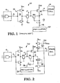
- CMOS high voltage switch adapted for connection between a decoder output and an EPROM cell is illustrated in Figure 1 of the drawings and has been labelled "Prior Art".
- This prior art switch suffers from the disadvantage that both the low voltage signal path and the high voltage signal path are through the same transistors; namely, P-channel MOS transistor P4 and N-channel MOS transistor N3. Due to the fact that these transistors are connected in series, their turn-on resistance values are relatively high. As a result, the operating speed of the switch is relatively slow.
- the voltage at the output node 4 will be one threshold voltage drop below the supply potential VCC. Therefore, the full supply potential will not be obtainable at the output node without modifying the switch design to include intrinsic or depletion-mode type transistors. However, the increased processing cost in fabricating such transistors makes this design change unacceptable.
- CMOS high voltage switch for interfacing between a decoder output and an ' input to an erasable, programmable read-only-memory which has two separate signal paths.
- CMOS high voltage switch which has a first signal path to accommodate a high voltage during a programming mode of operation and a second signal path to accommodate a low voltage during a read mode of operation.
- CMOS high voltage switch which includes a switching device connected to an output node for allowing the output node to be pumped up to a first higher voltage during a first mode of operation and for maintaining the output node at a second lower voltage during a second mode of operation.
- CMOS high voltage switch which includes a switching device formed of a P-channel MOS switching transistor and a P-channel MOS current-limiting transistor for switching an output node between first and second modes of operation.
- One aspect of the present invention is concerned with the provision of a CMOS high voltage switch for interfacing between a decoder output and an input to an erasable, programmable read-only-memory which includes an input means for receiving an input signal from the output of the decoder.
- a control device is provided which has a conduction path and a gate electrode. One end of the conduction path is connected to the output of the input means. The other end of the conduction path is connected to an output node. The gate electrode is connected to a supply potential.
- a pumping means is connected to the other end of the conduction path for pumping the output node to a first higher voltage during a first mode of operation. Switching means is also connected to the other end of the conduction path for switching the output node to a second lower voltage during a second mode of operation.
- Figure 1 a schematic circuit diagram of a conventional CMOS high voltage switch 10 of the prior art which is interconnected between the output of a decoder 12 and the input of an erasable, programmable read-only-memory (EPROM) 14.
- EPROM erasable, programmable read-only-memory
- the output of the decoder at node 2 is connected to the input of the high voltage switch 10.
- the decoder 12 When the decoder 12 has been selected, its output is at a low or "0" logic level on the order of 0 volts.
- the decoder When the decoder has not been selected, its output is at a high or "1" logic level which is approximately +5 volts.
- the output of the high voltage switch 10 at node 4 is connected to the input of the EPROM 14.
- the high voltage switch comprises an input means 15, a control device 17, and a pumping means 19.
- the input means 15 consist of a CMOS inverter 16 formed of a P-channel MOS transistor P4 and a N-channel MOS transistor N1 whose gate electrodes are connected together and to the input node 2 for receiving an input signal from the decoder 12.
- the common gate electrodes define the input of the inverter 16.
- the drain electrodes of the transistors P4 and N1 are also connected together and define the output of the inverter 16.
- the source of the transistor P4 is connected to a first lower supply potential VCC which is typically operated at +5 volts, and the source of the transistor N1 is connected to a ground potential.
- the control device 17 comprises a N-channel MOS pass transistor N3 having a conduction path and a gate electrode.
- the drain and source electrodes of the transistor N3 define the respective ends of the conduction path.
- the transistor N3 has it gate connected to the first lower supply potential VCC, its drain connected to the output of the inverter 16, and its source connected to the output node 4.
- the pumping means 19 includes a N-channel MOS transistor N2 having its gate electrode connected to the source of the pass transistor N3 and its drain electrode connected to a second higher potential VPP.
- the second supply potential VPP is typically operated at approximately +10 volts during a program or write mode of operation and is typically operated at approximately +5 volts during a read operation.
- the transistor N2 serves has a current-limiting resistor.
- the source of the transistor N2 is connected to the drain and gate electrodes of a N-channel MOS charge transfer transistor -N5 functioning as a diode and to one end of a capacitor C.
- the other end of the capacitor C is connected to a input node 18 for receiving pulses PUMPX from a free-running oscillator 20.
- the source of the charge transfer transistor N5 is connected to the source of the pass transistor N3.
- the P-channel transistor P4 is caused to be turned on so that the drain of the pass transistor N3 will be at the level of the first lower supply potential VCC. Since this lower supply potential VCC is also applied to the gate of the pass transistor N3, it will turn on and the output node 4 of the high voltage switch will be initially at one threshold voltage drop below the lower supply potential VCC. Further, the node 3 will be at two threshold voltage drops below the lower supply potential VCC or . approximately +3 volts. This is assuming that each threshold voltage drop is approximately +1 volt.
- the voltage at the node 3 will begin to be pumped up by the oscillator 20 via the capacitor C from this voltage of approximately +3 volts.
- the voltage at node 4 will be pumped toward the second supply potential VPP and will reach the same in its final condition.
- the P-channel transistor P4 is again caused to be turned on so that the drain of the pass transistor N3 will be at the first supply potential VCC. Again, the pass transistor N3 will be turned on so that the output node 4 will remain at one threshold voltage drop below the supply potential VCC.
- the input signal from the decoder 12 must be feed through the series connection of the P-channel transistor P4 and the N-channel pass transistor N3 in both the program mode of operation and the read mode of operation. Since the turn-on resistance values of the transistors P4 and N3 are relatively quite high, the operating speed of the high voltage switch 10 is reduced. Further, during the read mode the final voltage at the output node 4 does not reach the full first lower supply potential VCC due to the loss of a threshold voltage drop due to the pass transistor N3.
- FIG 2 is a schematic circuit diagram of a high voltage switch 110 of the present invention which is implemented with all CMOS transistors.
- the high voltage switch 110 is an improvement over the switch 10 of Figure 1 and provides two separate signal paths wherein a first one is used during the programming mode of operation and a second one is used during the read mode of operation.
- the high voltage switch 110 comprises all of the circuit elements contained in the input means 15, the control device 17 and the pumping means 19 of the switch 10 with the additional components of three P-channel MOS transistors P1, P6 and P7 and one N-channel MOS transistor N8.
- the components which are the same or function in the same way as in Figure 1 have been given the same reference numerals and are generally not explained again.
- the high voltage switch 110 utilizes the switch 10 of Figure 1 and further comprises switching means 22 and level-shifting means 24.
- the switching means 22 is formed by the P-channel MOS switching transistor P1 and the P-channel MOS current-limiting transistor P6.
- the transistor P1 has its source connected to the first lower supply potential VCC, its gate connected to a logic voltage VPXC and its drain connected to the source of the transistor P6.
- the gate of the transistor P6 is connected to the output of the decoder 12, and the drain of the transistor P6 is connected to the output node 4 which is connected to the gate of the transistor N2 and the source of the transistor N3.
- the level shifting means 24 is formed by the P-channel MOS current-limiting transistor P7 and the N-channel MOS charge transfer transistor N8.
- the current-limiting transistor P7 has its source connected to the first lower supply potential VCC and its gate connected to the output of the decoder 12.
- the drain of the transistor P7 is connected to the gate and drain electrodes of the charge transfer transistor N8 which functions as a diode.
- the source of the transistor N8 is connected to the gate and drain electrodes of the N-channel charge transfer transistor N5 (node 3).
- the second higher supply potential VPP will be operated at +10 volt and the logic voltage VPXC at input terminal 26 will be at a high logic level so as to turn off the switching transistor P1.
- the transistor P4 With the decoder 12 being selected, the transistor P4 will be turned on so that the drain of the pass transistor N3 will be at the first lower supply potential VCC. With the gate of the transistor N3 being tied to the supply potential VCC, it will be turned on so that the output node 4 will be one threshold voltage drop below the supply potential VCC. However, the node 3 will also be at one threshold voltage drop below the supply potential VCC due to the fact that transistors P7 and N8 will be turned on.
- node 3 will be at approximately +4 volts. As a result, the voltage at the node 3 will begin to be pumped up from this voltage of +4 volts instead of +3 volts of Figure 1. Thus, the voltage at node 3 in Figure 2 will be pumped up and reach the second supply potential VPP sooner than in Figure 1 thereby effecting a higher speed of operation.
- the second supply potential VPP will be operated at +5 volts and the logic voltage VPXC at the input terminal 26 will be at a low logic level so as to turn on the transistor P1. Since the transistor P6 is also turned on, the full supply potential VCC will reach the output node 4 without the loss of a threshold voltage drop.
- the input signal through the transistor P4 and the pass transistor N3 defining the first signal path is not used when the decoder 12 has been selected and is used only when the decoder has been deselected.
- a second signal path is used for turning on the switching transistor P1 so as to achieve a higher speed of operation as well as to improve latch-up immunity.
- the present invention provides improved CMOS high voltage switch which includes a first signal path to accommodate a high voltage during a programming mode of operation and a second signal path to accommodate a low voltage during a read mode of operation, thereby increasing its speed of operation and improving latch-up immunity.
- the high voltage switch of the present invention includes switching means connected to an output node for allowing the output node to be pumped up to a first higher voltage during the first mode of operation and for switching the output mode to a second lower voltage during the second mode of operation.
Landscapes
- Electronic Switches (AREA)
- Read Only Memory (AREA)
- Logic Circuits (AREA)
Applications Claiming Priority (2)
| Application Number | Priority Date | Filing Date | Title |
|---|---|---|---|
| US745568 | 1985-06-17 | ||
| US06/745,568 US4689495A (en) | 1985-06-17 | 1985-06-17 | CMOS high voltage switch |
Publications (2)
| Publication Number | Publication Date |
|---|---|
| EP0206710A2 true EP0206710A2 (de) | 1986-12-30 |
| EP0206710A3 EP0206710A3 (de) | 1988-10-26 |
Family
ID=24997255
Family Applications (1)
| Application Number | Title | Priority Date | Filing Date |
|---|---|---|---|
| EP86304612A Ceased EP0206710A3 (de) | 1985-06-17 | 1986-06-16 | CMOS Hochspannungsschalter |
Country Status (3)
| Country | Link |
|---|---|
| US (1) | US4689495A (de) |
| EP (1) | EP0206710A3 (de) |
| JP (1) | JPS61290817A (de) |
Cited By (2)
| Publication number | Priority date | Publication date | Assignee | Title |
|---|---|---|---|---|
| EP0288075A3 (en) * | 1987-04-24 | 1990-10-17 | Kabushiki Kaisha Toshiba | Sub-booster circuit for raising output voltage of main booster circuit |
| EP0362715A3 (de) * | 1988-10-06 | 1991-07-03 | STMicroelectronics S.r.l. | Speicher mit einer programmierbaren statischen Wahlschaltung für programmierbare Anordnungen |
Families Citing this family (26)
| Publication number | Priority date | Publication date | Assignee | Title |
|---|---|---|---|---|
| EP0209805B1 (de) * | 1985-07-22 | 1993-04-07 | Hitachi, Ltd. | Halbleitereinrichtung mit bipolarem Transistor und Isolierschicht-Feldeffekttransistor |
| US5197033A (en) * | 1986-07-18 | 1993-03-23 | Hitachi, Ltd. | Semiconductor device incorporating internal power supply for compensating for deviation in operating condition and fabrication process conditions |
| JPS6252797A (ja) * | 1985-08-30 | 1987-03-07 | Mitsubishi Electric Corp | 半導体記憶装置 |
| IT1204375B (it) * | 1986-06-03 | 1989-03-01 | Sgs Microelettronica Spa | Generatore di polarizzazione di sorgenti per transistori naturali in circuiti integrati digitali in tecnologia mos |
| US4814647A (en) * | 1987-04-06 | 1989-03-21 | Texas Instruments Incorporated | Fast rise time booting circuit |
| US4805152A (en) * | 1987-09-03 | 1989-02-14 | National Semiconductor Corporation | Refresh cell for a random access memory |
| US4943961A (en) * | 1988-05-05 | 1990-07-24 | Rca Licensing Corporation | Memory retention system for volatile memory devices |
| JPH077912B2 (ja) * | 1988-09-13 | 1995-01-30 | 株式会社東芝 | 昇圧回路 |
| US4954731A (en) * | 1989-04-26 | 1990-09-04 | International Business Machines Corporation | Wordline voltage boosting circuits for complementary MOSFET dynamic memories |
| US4999529A (en) * | 1989-06-30 | 1991-03-12 | At&T Bell Laboratories | Programmable logic level input buffer |
| US4963765A (en) * | 1989-07-03 | 1990-10-16 | Texas Instruments Incorporated | High speed CMOS transition detector circuit |
| KR950004745B1 (ko) * | 1990-01-23 | 1995-05-06 | 니뽄 덴끼 가부시끼가이샤 | 반도체 디지탈 회로 |
| US5038325A (en) * | 1990-03-26 | 1991-08-06 | Micron Technology Inc. | High efficiency charge pump circuit |
| US5023465A (en) * | 1990-03-26 | 1991-06-11 | Micron Technology, Inc. | High efficiency charge pump circuit |
| US5157280A (en) * | 1991-02-13 | 1992-10-20 | Texas Instruments Incorporated | Switch for selectively coupling a power supply to a power bus |
| KR940008206B1 (ko) * | 1991-12-28 | 1994-09-08 | 삼성전자 주식회사 | 고전압 스위치 회로 |
| GB2291296B (en) * | 1991-12-28 | 1996-04-17 | Samsung Electronics Co Ltd | Switching circuit |
| JP3890614B2 (ja) * | 1995-06-19 | 2007-03-07 | 富士通株式会社 | 昇圧電圧供給回路 |
| JP3431774B2 (ja) * | 1995-10-31 | 2003-07-28 | ヒュンダイ エレクトロニクス アメリカ | 混合電圧システムのための出力ドライバ |
| US5767734A (en) * | 1995-12-21 | 1998-06-16 | Altera Corporation | High-voltage pump with initiation scheme |
| JP4043060B2 (ja) * | 1996-06-14 | 2008-02-06 | 富士通株式会社 | トランジスタのしきい値補正回路及び半導体記憶装置並びにしきい値補正方法 |
| US6188265B1 (en) | 1997-12-12 | 2001-02-13 | Scenix Semiconduction, Inc. | High-voltage NMOS switch |
| US6388475B1 (en) * | 1999-12-29 | 2002-05-14 | Intle Corporation | Voltage tolerant high drive pull-up driver for an I/O buffer |
| US6559690B2 (en) * | 2001-03-15 | 2003-05-06 | Micron Technology, Inc. | Programmable dual drive strength output buffer with a shared boot circuit |
| JP4199765B2 (ja) * | 2005-12-02 | 2008-12-17 | マイクロン テクノロジー,インコーポレイテッド | 高電圧スイッチング回路 |
| JP4357546B2 (ja) * | 2007-06-07 | 2009-11-04 | 株式会社東芝 | 半導体装置 |
Family Cites Families (10)
| Publication number | Priority date | Publication date | Assignee | Title |
|---|---|---|---|---|
| GB2089612B (en) * | 1980-12-12 | 1984-08-30 | Tokyo Shibaura Electric Co | Nonvolatile semiconductor memory device |
| GB2094086B (en) * | 1981-03-03 | 1985-08-14 | Tokyo Shibaura Electric Co | Non-volatile semiconductor memory system |
| JPS5891680A (ja) * | 1981-11-26 | 1983-05-31 | Fujitsu Ltd | 半導体装置 |
| US4441172A (en) * | 1981-12-28 | 1984-04-03 | National Semiconductor Corporation | Semiconductor memory core program control circuit |
| US4442481A (en) * | 1982-04-07 | 1984-04-10 | Honeywell Inc. | Low power decoder circuit |
| JPS58185091A (ja) * | 1982-04-24 | 1983-10-28 | Toshiba Corp | 昇圧電圧出力回路および昇圧電圧出力回路を備えたアドレスデコ−ド回路 |
| JPS59124095A (ja) * | 1982-12-29 | 1984-07-18 | Fujitsu Ltd | 半導体記憶装置 |
| EP0137245B1 (de) * | 1983-08-30 | 1990-03-14 | Kabushiki Kaisha Toshiba | Integrierte Halbleiterschaltung |
| JPS6052112A (ja) * | 1983-08-31 | 1985-03-25 | Toshiba Corp | 論理回路 |
| US4638182A (en) * | 1984-07-11 | 1987-01-20 | Texas Instruments Incorporated | High-level CMOS driver circuit |
-
1985
- 1985-06-17 US US06/745,568 patent/US4689495A/en not_active Expired - Lifetime
-
1986
- 1986-06-16 EP EP86304612A patent/EP0206710A3/de not_active Ceased
- 1986-06-16 JP JP61141204A patent/JPS61290817A/ja active Pending
Cited By (2)
| Publication number | Priority date | Publication date | Assignee | Title |
|---|---|---|---|---|
| EP0288075A3 (en) * | 1987-04-24 | 1990-10-17 | Kabushiki Kaisha Toshiba | Sub-booster circuit for raising output voltage of main booster circuit |
| EP0362715A3 (de) * | 1988-10-06 | 1991-07-03 | STMicroelectronics S.r.l. | Speicher mit einer programmierbaren statischen Wahlschaltung für programmierbare Anordnungen |
Also Published As
| Publication number | Publication date |
|---|---|
| EP0206710A3 (de) | 1988-10-26 |
| US4689495A (en) | 1987-08-25 |
| JPS61290817A (ja) | 1986-12-20 |
Similar Documents
| Publication | Publication Date | Title |
|---|---|---|
| US4689495A (en) | CMOS high voltage switch | |
| US4866304A (en) | BICMOS NAND gate | |
| US4689504A (en) | High voltage decoder | |
| US5073726A (en) | Input circuit of semiconductor integrated circuit and semiconductor integrated circuit having input circuit | |
| US4812679A (en) | Power-on reset circuit | |
| US4577124A (en) | CMOS Logic circuit | |
| KR920010819B1 (ko) | 레벨 변환 기능을 갖는 출력버퍼회로 | |
| US6127841A (en) | CMOS buffer having stable threshold voltage | |
| US4390803A (en) | Semiconductor driver circuit | |
| US4698530A (en) | Power switch for dual power supply circuit | |
| KR960011964B1 (ko) | 출력버퍼장치 | |
| US5065361A (en) | Semiconductor memory integrated circuit | |
| US4638182A (en) | High-level CMOS driver circuit | |
| JPH0241838B2 (de) | ||
| JPH05175811A (ja) | パワーオンリセット回路 | |
| JPH0583004B2 (de) | ||
| US4542307A (en) | Double bootstrapped clock buffer circuit | |
| US7816969B2 (en) | Level shifter circuit | |
| EP0063357B1 (de) | Treiberschaltung | |
| US4806797A (en) | bi-CMOS buffer cascaded to CMOS driver having PMOS pull-up transistor with threshold voltage greater than VBE of bi-CMOS bipolar pull-up transistor | |
| US6756813B2 (en) | Voltage translator | |
| US4794280A (en) | Darlington bicmos driver circuit | |
| US4883979A (en) | Darlington BiCMOS driver circuit | |
| US5030860A (en) | Darlington BiCMOS driver circuit | |
| KR910003604B1 (ko) | 차아지업 및 디스차아지 회로를 이용한 기준전압 발생회로 |
Legal Events
| Date | Code | Title | Description |
|---|---|---|---|
| PUAI | Public reference made under article 153(3) epc to a published international application that has entered the european phase |
Free format text: ORIGINAL CODE: 0009012 |
|
| AK | Designated contracting states |
Kind code of ref document: A2 Designated state(s): AT BE CH DE FR GB IT LI LU NL SE |
|
| PUAL | Search report despatched |
Free format text: ORIGINAL CODE: 0009013 |
|
| AK | Designated contracting states |
Kind code of ref document: A3 Designated state(s): AT BE CH DE FR GB IT LI LU NL SE |
|
| 17P | Request for examination filed |
Effective date: 19890126 |
|
| 17Q | First examination report despatched |
Effective date: 19900906 |
|
| STAA | Information on the status of an ep patent application or granted ep patent |
Free format text: STATUS: THE APPLICATION HAS BEEN REFUSED |
|
| 18R | Application refused |
Effective date: 19910907 |
|
| RIN1 | Information on inventor provided before grant (corrected) |
Inventor name: LIU, WEI-TI |