EP0209805B1 - Halbleitereinrichtung mit bipolarem Transistor und Isolierschicht-Feldeffekttransistor - Google Patents
Halbleitereinrichtung mit bipolarem Transistor und Isolierschicht-Feldeffekttransistor Download PDFInfo
- Publication number
- EP0209805B1 EP0209805B1 EP86109470A EP86109470A EP0209805B1 EP 0209805 B1 EP0209805 B1 EP 0209805B1 EP 86109470 A EP86109470 A EP 86109470A EP 86109470 A EP86109470 A EP 86109470A EP 0209805 B1 EP0209805 B1 EP 0209805B1
- Authority
- EP
- European Patent Office
- Prior art keywords
- potential
- circuit
- channel mosfet
- node
- source
- Prior art date
- Legal status (The legal status is an assumption and is not a legal conclusion. Google has not performed a legal analysis and makes no representation as to the accuracy of the status listed.)
- Expired - Lifetime
Links
- 239000004065 semiconductor Substances 0.000 title claims description 28
- 230000005669 field effect Effects 0.000 title claims description 6
- 230000015654 memory Effects 0.000 claims description 33
- 239000000872 buffer Substances 0.000 claims description 10
- 230000008859 change Effects 0.000 claims description 4
- 230000004044 response Effects 0.000 claims description 3
- 238000010586 diagram Methods 0.000 description 37
- 229920006395 saturated elastomer Polymers 0.000 description 10
- 230000015556 catabolic process Effects 0.000 description 7
- 230000000052 comparative effect Effects 0.000 description 7
- 239000003990 capacitor Substances 0.000 description 4
- 101710130550 Class E basic helix-loop-helix protein 40 Proteins 0.000 description 3
- 102100025314 Deleted in esophageal cancer 1 Human genes 0.000 description 3
- 230000008901 benefit Effects 0.000 description 3
- 230000006870 function Effects 0.000 description 3
- 230000003071 parasitic effect Effects 0.000 description 3
- 238000007599 discharging Methods 0.000 description 2
- 238000004519 manufacturing process Methods 0.000 description 2
- 230000004048 modification Effects 0.000 description 2
- 238000012986 modification Methods 0.000 description 2
- 229910021420 polycrystalline silicon Inorganic materials 0.000 description 2
- 229920005591 polysilicon Polymers 0.000 description 2
- 238000009877 rendering Methods 0.000 description 2
- 230000000630 rising effect Effects 0.000 description 2
- 230000006641 stabilisation Effects 0.000 description 2
- 238000011105 stabilization Methods 0.000 description 2
- 230000003068 static effect Effects 0.000 description 2
- 230000001360 synchronised effect Effects 0.000 description 2
- XAGFODPZIPBFFR-UHFFFAOYSA-N aluminium Chemical compound [Al] XAGFODPZIPBFFR-UHFFFAOYSA-N 0.000 description 1
- 229910052782 aluminium Inorganic materials 0.000 description 1
- 239000000969 carrier Substances 0.000 description 1
- 230000000295 complement effect Effects 0.000 description 1
- 230000003247 decreasing effect Effects 0.000 description 1
- 230000001419 dependent effect Effects 0.000 description 1
- 230000000694 effects Effects 0.000 description 1
- 230000036039 immunity Effects 0.000 description 1
- 230000002093 peripheral effect Effects 0.000 description 1
- 230000009467 reduction Effects 0.000 description 1
Images






Classifications
-
- G—PHYSICS
- G11—INFORMATION STORAGE
- G11C—STATIC STORES
- G11C8/00—Arrangements for selecting an address in a digital store
- G11C8/10—Decoders
-
- G—PHYSICS
- G11—INFORMATION STORAGE
- G11C—STATIC STORES
- G11C7/00—Arrangements for writing information into, or reading information out from, a digital store
- G11C7/12—Bit line control circuits, e.g. drivers, boosters, pull-up circuits, pull-down circuits, precharging circuits, equalising circuits, for bit lines
-
- H—ELECTRICITY
- H03—ELECTRONIC CIRCUITRY
- H03K—PULSE TECHNIQUE
- H03K17/00—Electronic switching or gating, i.e. not by contact-making and –breaking
- H03K17/51—Electronic switching or gating, i.e. not by contact-making and –breaking characterised by the components used
- H03K17/56—Electronic switching or gating, i.e. not by contact-making and –breaking characterised by the components used by the use, as active elements, of semiconductor devices
- H03K17/687—Electronic switching or gating, i.e. not by contact-making and –breaking characterised by the components used by the use, as active elements, of semiconductor devices the devices being field-effect transistors
- H03K17/693—Switching arrangements with several input- or output-terminals, e.g. multiplexers, distributors
-
- H—ELECTRICITY
- H03—ELECTRONIC CIRCUITRY
- H03K—PULSE TECHNIQUE
- H03K19/00—Logic circuits, i.e. having at least two inputs acting on one output; Inverting circuits
- H03K19/01—Modifications for accelerating switching
- H03K19/017—Modifications for accelerating switching in field-effect transistor circuits
-
- H—ELECTRICITY
- H03—ELECTRONIC CIRCUITRY
- H03K—PULSE TECHNIQUE
- H03K19/00—Logic circuits, i.e. having at least two inputs acting on one output; Inverting circuits
- H03K19/0175—Coupling arrangements; Interface arrangements
- H03K19/017509—Interface arrangements
- H03K19/017518—Interface arrangements using a combination of bipolar and field effect transistors [BIFET]
-
- H—ELECTRICITY
- H03—ELECTRONIC CIRCUITRY
- H03K—PULSE TECHNIQUE
- H03K19/00—Logic circuits, i.e. having at least two inputs acting on one output; Inverting circuits
- H03K19/02—Logic circuits, i.e. having at least two inputs acting on one output; Inverting circuits using specified components
- H03K19/08—Logic circuits, i.e. having at least two inputs acting on one output; Inverting circuits using specified components using semiconductor devices
- H03K19/094—Logic circuits, i.e. having at least two inputs acting on one output; Inverting circuits using specified components using semiconductor devices using field-effect transistors
- H03K19/0944—Logic circuits, i.e. having at least two inputs acting on one output; Inverting circuits using specified components using semiconductor devices using field-effect transistors using MOSFET or insulated gate field-effect transistors, i.e. IGFET
- H03K19/09448—Logic circuits, i.e. having at least two inputs acting on one output; Inverting circuits using specified components using semiconductor devices using field-effect transistors using MOSFET or insulated gate field-effect transistors, i.e. IGFET in combination with bipolar transistors [BIMOS]
-
- H—ELECTRICITY
- H03—ELECTRONIC CIRCUITRY
- H03K—PULSE TECHNIQUE
- H03K5/00—Manipulating of pulses not covered by one of the other main groups of this subclass
- H03K5/01—Shaping pulses
- H03K5/08—Shaping pulses by limiting; by thresholding; by slicing, i.e. combined limiting and thresholding
-
- H—ELECTRICITY
- H03—ELECTRONIC CIRCUITRY
- H03K—PULSE TECHNIQUE
- H03K2217/00—Indexing scheme related to electronic switching or gating, i.e. not by contact-making or -breaking covered by H03K17/00
- H03K2217/0036—Means reducing energy consumption
Definitions
- the present invention relates to a semiconductor memory device according to the preamble of claim 1, and more particularly to a word line driver circuit employing a bipolar transistor and an insulated gate field effect transistor (hereinbelow, termed 'IGFET') which is well-suited to attain a high driving capability and a large output amplitude.
- 'IGFET' insulated gate field effect transistor
- Fig. 1A is a circuit diagram of the semiconductor device. The operation of the circuit and the problem thereof will be explained with reference to Fig. 1A.
- This semiconductor device consists of the parallel connection between a circuit composed of CMOS (complementary MOS) transistors 4, 5 and a bipolar transistor 7 and a circuit composed of an IGFET 6 and a bipolar transistor 8.
- V SS of a lower source shall be assumed O V.
- the P-channel IGFET 4 turns “on” and current flows to the base of the bipolar transistor 7, so that this bipolar transistor 7 turns “on”.
- the bipolar transistor 8 does not turn "on” because the potential of the base thereof is O V.
- Fig. 1B is a diagram showing the circuit arrangement of the semiconductor device.
- the circuit in Fig. 1B is such that circuits composed of symmetrically arranged CMOS inverter circuits and bipolar transistors are connected in parallel across input and output nodes.
- the foregoing circuit in Fig. 1A delivers a signal having an inversive phase to the phase of an input, whereas the circuit in Fig. 1B delivers a signal having the same phase as that of an input. More specifically, when the input node I becomes a high level, an IGFET 13 turns “on” and current flows to the base of a bipolar transistor 17, so that this bipolar transistor 17 turns "on".
- a circuit shown in Fig. 1C is disclosed in the official gazette of Japanese Patent Application Laid-open No. 59-8431.
- a base current flows from a power source V CC to a bipolar transistor Q 2A through a P-channel IGFET M 2A , to turn "on" the transistor Q 2A , so that an output node O becomes a high level.
- the collector potential of the bipolar transistor Q 2A becomes lower than the potential of the power source V CC by the product between the collector current and a parasitic collector resistance in the bipolar transistor Q 2A and a resistance parasitic to external collector wiring (both being omitted from illustration for the sake of brevity). Accordingly, when the collector resistance of the bipolar transistor Q 2A is great, the base potential of this transistor Q 2A might become higher than the collector potential thereof to establish the so-called saturation state. As is well known, when the bipolar transistor falls into the saturation state, large quantities of minority carriers are stored in the base, and a long time is required for turn-off.
- the above object is solved by the invention characterized in claim 1.
- the invention is based on the idea that the resistance and capacitance of a word line is a main factor limiting the operating speed of the memory.
- the word lines are preferentially made of polysilicon rather than aluminum although polysilicon has a higher resistance.
- the invention uses a word line driver employing a bipolar transistor which is capable of supplying particularly high currents and high voltages.
- Figs. 1A to 1C are circuit diagrams each showing a prior art.
- Figs. 2 to 5 are diagrams for explaining a first embodiment of the present invention.
- Fig. 6 is a diagram for explaining a second embodiment of the present invention.
- Figs. 7 and 8 are diagrams for explaining a third embodiment of the present invention.
- Fig. 9 is a diagram for explaining a fourth embodiment of the present invention.
- Figs. 10A to 14 are diagrams for explaining a fifth embodiment of the present invention.
- Figs. 15A to 19 are diagrams for explaining a sixth embodiment of the present invention.
- Figs. 20 to 26 are diagrams for explaining a seventh embodiment of the present invention.
- Figs. 27 to 29 are diagrams for explaining an eighth embodiment of the present invention.
- Fig. 30 is a diagram for explaining a ninth embodiment of the present invention.
- Figs. 31 and 32 are diagrams for explaining a tenth embodiment of the present invention.
- Figs. 33 and 34 are diagrams for explaining an eleventh embodiment of the present invention.
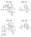
- Fig. 35 is a diagram for explaining a twelfth embodiment of the present invention.
- Fig. 36 is a diagram for explaining a thirteenth embodiment of the present invention.
- Figs. 37 and 38 are diagrams for explaining a comparative example.
- Figs. 39 and 40 are diagrams for explaining a fourteenth embodiment of the present invention.
- Fig. 41 is a diagram for explaining a fifteenth embodiment of the present invention.
- Fig. 42 is a diagram for explaining a sixteenth embodiment of the present invention.
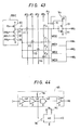
- Fig. 43 is a diagram for explaining a further comparative example.
- Fig. 44 is a diagram for explaining a further comparative example.
- Fig. 2 is a diagram of an embodiment for explaining the concept of the semiconductor device of the present invention. Shown in Fig. 2 is a case of a circuit having one input and one output.
- letter D denotes a combined circuit which includes bipolar transistors and IGFETs (or MIS or MOS transistors), while letter C denotes a preceding circuit which controls the circuit D.
- Letter A indicates a node to which the reference voltage of the operation of the circuit C is applied, and symbols B1 - B n indicate nodes to which the reference voltages of the operation of the circuit D are applied.
- letter E indicates the input node of the circuit C, and letter G the output node of the circuit D.
- a connection line F is a signal line for transmitting a signal for controlling the circuit D, from the circuit C.
- At least one of the voltages to be applied to the nodes B1 - B n is set higher than the voltage to be applied to the node A, whereby the level of a signal to be output to the node G is made higher than the level of the signal which is input to the circuit D through the signal line F.
- the level of a signal to be output to the node G is made higher than the level of the signal which is input to the circuit D through the signal line F.
- the voltages to be applied to the node A and the nodes B1 - B n may be oens of fixed levels or pulses as are needed, and in some cases, a plurality of reference voltages may be fed to the circuit C.
- a plurality of signal lines F may well be laid.
- the present invention is not restricted to the arrangement of Fig. 2, but it is also applicable to a multi-input and multi-output circuit. For the sake of brevity, however, embodiments based on the same arrangement as in Fig. 2 will be described below. It is assumed that, as the circuit C, a CMOS inverter as shown at C in Fig. 3 be used. In the inverter C in Fig. 3, a node A is connected to an upper source voltage V A , but this is not restrictive as stated before.
- Fig. 3 is an arrangement diagram of a semiconductor device showing the details of the first embodiment of the present invention.
- the reference pulse voltage of the operation of a circuit D is applied to a node B1, and a level higher than the operating reference voltage V A of the preceding circuit C is delivered to an output node G.
- an N-channel IGFET 27 turns “on” to bring the base of a bipolar transistor 26 into O V, and the bipolar transistor 26 turns “off” to turn “on” an N-channel IGFET 29, so that the potential of the output node G becomes O V.
- the potential of the input node E is raised to V A to lower the potential of the signal line F (refer to Fig. 3) and to raise the potential of the node B1 to or above V A .
- the P-channel IGFET 25 turns “on”
- the N-channel IGFET 27 turns “off”.
- the N-channel IGFET 29 turns “off", so that current flows to the output node G to raise the potential thereof.
- the potential of the output node G arrives at a value which is obtained by subtracting the base-emitter forward voltage V BE of the bipolar transistor 26 from the potential of the base thereof. Therefore, when a desired output level at the output node G is denoted by V A + V ⁇ (V ⁇ ⁇ O) , it is obtained by boosting the potential of the node B1 to V A + V ⁇ + V BE .
- the potential of the signal line F rises to V A as stated before, to turn “off” the bipolar transistor 26 and to turn “on” the N-channel IGFET 29, so that the potential of the output node G becomes O V.
- the potential of the node B1 at this time can be set at any desired value not greater than V A +
- the potential of the node B1 to be applied when the signal received from the signal line F is the low voltage is set at will, whereby the output of the high voltage can be produced while the feature of high operating speed of the bipolar transistor is kept.
- the N-channel IGFET 29 for lowering the potential of the output node G can be replaced with an arrangement shown at numeral 30 in Fig. 5. That is, the circuit D comes to have an arrangement in which combinations each consisting of the inverse CMOS transistors and the bipolar transistor are connected in parallel. In this case, current flowing through an N-channel IGFET 40 is amplified by a bipolar transistro 42, so that the lowering of the potential of the output node can be effected fast.
- the potential of the output node G does not lower perfectly to O V because it is limited by the base-emitter forward voltage of the bipolar transistor 42.
- the arrangement 30 in Fig. 5 may be disposed in parallel with the N-channel IGFET 29 in Fig. 3.
- a P-channel IGFET 41 serves to discharge charges stored in the base of the bipolar transistor 42 when the signal line F was O V and to reliably turn "off" this bipolar transistor 42.
- Fig. 6 is an arrangement diagram of a semiconductor device showing a second embodiment of the present invention.
- the collector of the bipolar transistor 52 is connected to the node B2 and can have its potential set independently of the node B1 for feeding the current to the base 55 of this transistor.
- this bipolar transistor 52 can be reliably prevented from getting saturated.
- a pulse voltage having an amplitude not smaller than the base voltage of the bipolar transistor 52 may be impressed on the node B2 in synchronism with the potential fluctuation of the base 55, or the potential of the node B2 may be held at a fixed value higher than the upper limit of the potential of the base 55.
- the bipolar transistor 52 might be deeply saturated temporarily due to the fluctuation of a supply voltage, etc., a diode DIO may be inserted between the nodes B1 and B2 as shown in the figure, whereby when the potential of the node B1 has become abnormally high, current is caused to flow through the diode so as to prevent the deep saturation of the bipolar transistor 52.
- the circuit 30 for lowering the potential of the output node G may be constructed, as is necessary, of only the IGFET 29 as shown in Fig. 3, of the bipolar transistor and the IGFETs as shown in Fig. 5, or of the two connected in parallel.
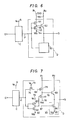
- Fig. 7 is an arrangement diagram of a semiconductor device showing a third embodiment of the present invention.
- circuit D performs the so-called inversive operation of delivering a signal having the inversive phase to the phase of a signal received from the signal line F
- a circuit D performs the so-called non-inversive operation of delivering a signal having the same phase as that of an input F.
- a bipolar transistor 83 is a transistor for supplying current to an output node G so as to raise the potential of this node G.
- An N-channel IGFET 84 is a transistor for pouring current from the output node G to a lower source voltage V SS so as to lower the potential of this node G.
- the other IGFETs serve to control the on/off of the bipolar transistor 83 and the IGFET 84.
- the potential of a node B2 is assumed to be held at a fixed value higher than the upper limit value of the potential of the base 76 of the bipolar transistor 83.
- a pulse voltage synchronized with the potential fluctuation of the base 76 may well be applied within a range within which the bipolar transistor 83 is not saturated.
- the potential of an input node E be V A
- the potential of the signal line F is rendered O V by a circuit C, and hence, the N-channel IGFET 75 turns “off”, the P-channel IGFET 80 turns “on” and the N-channel IGFET 81 turns “off”, so that the potential of a part 87 becomes V A .
- the N-channel IGFET 77 turns “on”
- the bipolar transistor 83 turns “off”
- the N-channel IGFET 84 turns “on”, so that the output node G becomes O V.
- the potential of the signal line F becomes V A
- the gate 88 of the N-channel IGFET 75 is charged to a voltage which is obtained by subtracting the threshold voltage of the N-channel IGFET 74 from the potential V A .
- the P-channel IGFET 80 turns “off” and the N-channel IGFET 81 turns “on”, so that the potential of the part 87 becomes O V
- the N-channel IGFETs 84 and 77 turn “off".
- the gate 88 of the N-channel IGFET 75 is boosted to a potential higher than that of the node B1 by the self-capacitance between the gate 88 and the node B1 because the gate 88 of the IGFET 75 has been previously charged to the voltage obtained by subtracting the threshold voltage of the N-channel IGFET 74 from V A . For this reason, current flows to the base 76 of the bipolar transistor 83, and the potential of this base 76 rises up to the potential of the node B1 without being limited by the threshold voltage of the N-channel IGFET 75.
- the potential of the output node G rises up to a value which is obtained by subtracting the base-emitter forward voltage V BE of the bipolar transistor 83 from the potential of the node B1.
- V BE base-emitter forward voltage
- the potential of the node B1 may be made V A + V ⁇ + V BE . Since the N-channel IGFET 74 has the voltage of its gate 73 set at V A , it turns "off" and functions to prevent the counter flow of current from the gate 88 to the signal line F when the gate 88 has been boosted to or above V A .
- the circuit in Fig. 5 may be used or the circuit in Fig. 5 and the N-channel IGFET 84 connected in parallel may well be used as is necessary.
- a diode may be connected between the nodes B1 and B2 as shown in Fig. 6, to prevent the potential of the node B1 from abnormally rising relative to that of the node B2.
- Fig. 9 is an arrangement diagram of a semiconductor device showing a fourth embodiment of the present invention.
- Fig. 7 The point of the greatest difference in circuitry between Fig. 7 and Fig. 9 is that, in Fig. 7, the collector and base of the bipolar transistor 83 are electrically isolated, whereas in Fig. 9, an N-channel IGFET 103 is inserted between the collector and base of a bipolar transistor 104 so as to feed a base current and a collector current from a node B2.
- V BE denotes the base-emitter forward voltage of the bipolar transistor 104.
- V T102 and V T103 denote the threshold voltages of the N-channel IGFETs 102 and 103 respectively, the base potential of the bipolar transistor 104 rises only to V A - V T102 - V T103 , and the potential of the output G further drops by V BE . In this condition left intact, accordingly, an output level not lower than V A cannot be produced.
- a pulse voltage is impressed on the node B1 under the state under which the gate 112 has been charged, whereby the potential of the gate 112 is boosted to or above V A + V ⁇ + V BE + V T103 by a capacitor 100.
- the base potential of the bipolar transistor 104 rises up to V A + V ⁇ + V BE , and the potential of the output node G reaches the desired output level V A + V ⁇ .
- the base potential of the bipolar transistor 104 rises only to the level equal to that of the node B2. Therefore, even when the potential of the node B2 has lowered for any cause, the bipolar transistor 104 is not saturated.
- a signal line F becomes O V.
- N-channel IGFETs 103 and 107 turn “off"
- P-channel IGFET 106 turns “on”
- the N-channel IGFET 105 turns “off”.
- the bipolar transistor 104 turns “off” and the N-channel IGFET 108 turns “on”, so that the potential of the output node G becomes O V.
- a circuit 30 for lowering the potential of the output node G may have the arrangement of Fig. 5 or may well have the circuit of Fig.
- the potential of the node B2 has been the fixed level of V A + V ⁇ + V BE
- a pulse voltage varying from O V to V A + V ⁇ + V BE may well be impressed on the node B2 after the gate 112 has been charged. Since, on this occasion, the potential of the gate 112 is boosted by the self-capacitance between the gate 112 of the N-channel IGFET 103 and the node B2, the capacitor 100 and the node B1 are not necessarily required.
- an operating reference voltage is set at a value different from the reference voltage of a preceding circuit which controls the above circuit, thereby making it possible to realize a semiconductor device which has a high output amplitude of or above the reference voltage of the preceding circuit while exploiting the high driving capability of the bipolar transistor to the utmost.
- a pulse voltage needs to be impressed on the node B1.
- circuits for generating pulse voltages the circuit arrangements of which are well known, and hence, they shall not be clearly shown here.
- a circuit which generates pulse voltages as shown by the voltage waveforms in Fig. 8 there is a circuit "256k CMOS Dynamic RAM with Static Column Mode of Cycle Time of 50 ns" by Ishihara, Miyazawa and Sakai, shown in 'Nikkei Electronics', February 11, 1985, pp. 243 - 263, Fig. 7.
- the source of a P-channel IGFET for example, 25 in Fig.
- a high voltage can act between the drain and source of an N-channel IGFET (for example, 29 in Fig. 3).
- the voltage acting between the drain and source of the N-channel IGFET which is problematic as to the breakdown voltage may be reduced in such a way that an N-channel IGFET whose gate potential is V A is inserted in series between the drain of the problematic N-channel IGFET and a node to which this drain is connected.
- the invention is particularly suitable for the word driver of a dynamic semiconductor memory.
- the reason is that the realization of a high-speed dynamic semiconductor memory requires to raise the signal-to-noise ratio by driving a selected word line at high speed and with a large amplitude and increasing a signal amplitude and also to raise the soft error immunity by increasing storage charges.
- Fig. 10A is a block diagram of the dynamic semiconductor memory, which shows a memory cell array MCA of N bits and peripheral circuits.
- i word lines WL and j data lines DL are laid out perpendicularly to each other, and memory cells MC are arranged at N of the intersection points between the word lines and the data lines.
- Address inputs X O - X n and Y O - Y m are respectively applied to address buffers ABX and ABY, the outputs of which are respectively transmitted to decoders/drivers XD and YD.
- the circuit XD of these decoders/drivers XD and YD drives the word line, and the circuit YD drives a write/read circuit RC, so as to write or read data into or from a selected memory cell MC in the memory cell array MCA.
- Symbol CC denotes a write/read control circuit, which controls the address buffers ABX, ABY, the decoders/drivers XD, YD, the write/read circuit RC and an output circuit OC in accordance with a chip select signal CS , a write enable signal WE and an input signal DI.
- the output circuit OC is a circuit which serves to deliver out the data read by the write/read circuit RC.
- the write/read circuit RC can also have a part thereof arranged at the end of the memory cell array MCA opposite to the decoder/driver YD so as to receive control signals from the decoder/driver YD by passing them over the memory cell array MCA.
- the X-group address inputs X O - X n and the Y-group address inputs Y O - Y m are applied from the separate input nodes in Fig. 10A, it is also possible to adopt the so-called 'address multiplex system' wherein these input nodes are shared and the inputs are applied with time differences as stated in, for example, 1977 ISSCC "Digest of Technical Papers", pp. 12 - 13.
- the aforementioned write/read control circuit may be driven in such a way that signals for controlling the acceptance of addresses, namely, the so-called RAS and CAS are substituted for the chip select signal CS .
- the memory cell MC may well be a static memory shown in Fig. 10B.
- Fig. 11 is a diagram of an embodiment in which the arrangement of Fig. 10A is put into a more concrete form, and which shows parts of the memory cell array MCA and the decoder/driver XD more specifically.
- DEC0 and DEC1 indicate decoders, WD0 and WD1 word drivers, WL0 and WL1 word lines, DL0 and DL0 a pair of data lines, and MC0 and MC1 memory cells.
- EQ indicates an equalizer for balancing the potentials of the data lines, in other words, a circuit for precharging the data lines to V A /2, and SA a sense amplifier.
- the decoders DEC0 and DEC1 operate with reference to a voltage V A applied to nodes 130 and 137 respectively.
- the word drivers WD0 and WD1 to which the present invention is applied operate with reference to a pulse voltage ⁇ X impressed on nodes 154 and 157, a voltage V H applied to nodes 155 and 158, and a pulse voltage ⁇ L impressed on nodes 156 and 159, respectively.
- the voltage V H is of course set at a potential which does not saturate bipolar transistors 150 etc.
- each of the word drivers WD0 and WD1 is the same as that of the circuit D in Fig. 7 except the fact that an N-channel IGFET 152 or 166 is disposed in parallel with an N-channel IGFET 151 or 165. Now, a reading operation in Fig. 11 will be described in conjunction with voltage waveforms in Fig. 12.
- the pair of data lines DL0 and DL0 are brought to equal potentials of about 1 ⁇ 2 V A by the equalizer EQ and are thereafter brought into floating states.
- a precharge signal ⁇ P is rendered O V to precharge the gates of N-channel IGFETs 148 and 164 to voltages obtained by subtracting the threshold voltages of N-channel IGFETs 145 and 163 from the voltage V A , respectively.
- ⁇ P is rendered O V to precharge the gates of N-channel IGFETs 148 and 164 to voltages obtained by subtracting the threshold voltages of N-channel IGFETs 145 and 163 from the voltage V A , respectively.
- the precharge signal ⁇ P is raised, whereupon either of the affirmative and negative of the address buffer outputs rises, in accordance with which some of N-channel IGFETs in the decoders DEC turn "on", and among the precharged gates of the IGFETs, those of unselected word drivers other than a word driver connected to a word line to be selected become O V. Illustrated here is a case where the word line WL0 is selected, and the gate of the N-channel IGFET 148 remains precharged. On the other hand, the gate of the N-channel IGFET 164 becomes O V because the word line WL1 is unselected.
- the unselected word line WL1 is fixed to O V in such a way that the N-channel IGFET 165 in the word driver WD1 turns "on".
- the gate of the N-channel IGFET 148 in the word driver WD0 is boosted because of the precharge, and the potential of the word line WL0 rises to V A + V ⁇ similarly to the circuit operation in Fig. 7.
- the gate of the N-channel IGFET 164 in the word driver WD1 is not boosted because of the voltage of O V, and this N-channel IGFET 164 remains "off", so that the potential of the word line WL1 remains at O V.
- an N-channel IGFET 160 in the memory cell MC0 turns "on"
- a signal is read out from the memory cell MC0 to the data line DL0, and a minute potential difference develops between the data line DL0 and the paired data line DL0 .
- the potential difference between the pair of data lines is amplified by the sense amplifier SA, and data is rewritten into the memory cell and is transmitted to a succeeding circuit. Subsequently, the pulse signal ⁇ X is lowered to O V and the latch signal ⁇ L is raised to lower the word line WL0 to O V, whereupon the pair of data lines are brought to the equal potentials of about 1 ⁇ 2 V A by the equalizer EQ. Meanwhile, all the address buffer outputs are lowered, and the precharge signal ⁇ P is lowered to O V to perform precharging so as to make ready for the next operation.
- the potential of the selected word line can be raised at high speed and with a large amplitude since the circuit of the present embodiment is applied to each of the word drivers WD0, WD1, ...... As a result, the signal voltage and the storage voltage of the memory cell can be increased, and a high speed operation and a high reliability are compatible.
- the circuit for generating the pulse signal ⁇ X the circuit contained in "Nikkei Electronics" referred to before may be employed, and in order to attain a still higher speed, the embodiment in Fig. 6 may well be employed by way of example. Besides, although in Fig.
- each word driver is provided with the decoder and the pulse signal ⁇ X is input to all the word drivers in common, various modifications are of course possible in such a manner that a single decoder is shared by a plurality of word drivers as is necessary and that the pulse signal of only one of the word drivers sharing the decoder is decoded and input.
- the precharge voltages of the data lines are not restricted thereto but can be set at will within a range of O - V A .
- the bipolar transistors in the unselected word drivers for example, the transistor 168 in the word driver WD1 have their bases held at O V by the signal ⁇ X when this signal is O V and by IGFETs inserted between the bases of the above bipolar transistors and a lower source voltage V SS , for example, a FET 167 in the word driver WD1 when the signal ⁇ X rises.
- the breakdown voltages of the above bipolar transistors are accordingly determined by BV CES as stated before, so that no problem is posed even when the collectors of the transistors are left intact at the high voltage V H .
- the arrangement of Fig. 11 requires the two upper voltage sources of the source for supplying the voltage V A and the source for supplying the voltage V H . It is of course possible to separately supply the source voltages from outside the chip, but it is also possible to externally supply only one of the voltages and to generate the other inside the chip with reference to the external voltage and supply the generated voltage or to generate both the source voltages inside the chip with reference to another voltage source. Accordingly, those of the embodiment of Fig.
- 11 and the preceding embodiments which require the two upper source voltages can also be constructed by the use of a single external upper voltage source in such a way that, by way of example, the higher one of the two voltages is fed directly from the external upper voltage source, while the lower one is fed by lowering the external upper source voltage by means of a voltage limiter circuit disclosed in any of the specifications of Japanese Patent Application No. 56-168698, Japanese Patent Application No. 57-220083, etc. In some cases, it is also allowed to feed the lower one of the two required source voltages from an external upper voltage source and to feed the higher one by raising the voltage of the external upper voltage source by means of a booster circuit.
- Fig. 13 is a diagram of one embodiment of a booster circuit for use in the present invention.
- the voltage V A is supplied from an external upper voltage source so as to generate the high voltage V H .
- the circuit in Fig. 13 is basically such that booster circuits CP1 and CP2 of the so-called charge pump type are arrayed in parallel. Since the operating principle of the charge pump type booster circuit is well known, it shall be omitted herefrom.
- a Zener diode 192 serves, when the voltage of a node 194 has become much higher than the desired level V H , to leak current and to prevent a further potential rise. However, it may be removed if it is not necessary.
- the Zener diode 192 may well be replaced with a plurality of ordinary diodes or MIS diode circuits each having the gate and drain of a MIS transistor connected, which are connected in the forward direction.
- Shown as each of the booster circuits CP1 and CP2 is an example in which MIS capacitors and diodes constructed of MIS transistors are connected in three stages.
- V T the threshold voltage of the MIS transistor
- V A the amplitudes of pulses ⁇ S1 - ⁇ S3 and ⁇ T1 - ⁇ T3
- a voltage to be produced becomes approximately (n + 1)(V A - V T ), and the value n may be selected according to the required value of V H .
- Fig. 14 is a diagram exemplifying the voltage waveforms of the pulses which are impressed on the booster circuits CP1 and CP2 in Fig. 13.
- the booster circuit CP1 operates during the standby period t st , and both the booster circuits CP1 and CP2 operate during the active period t op .
- the chip select signal CS or the RAS signal may be utilized.
- the booster circuit CP2 may of course be activated by utilizing the CAS signal or the like even after the word line potential has reached the high level.
- the saturation may be prevented in such a way that a diode is connected between the output node of the circuit for generating the pulse signal ⁇ X and the V H node 194 in Fig. 13 so as to turn "on" the diode when the potential of the pulse ⁇ X is high relative to the voltage V H as described before.
- the reference voltage of the operation thereof is set at a value different from that of the reference operating voltage of a preceding circuit for controlling the above circuit, so that the high driving capability of the bipolar transistor is sufficiently exploited, while at the same time a desired high output level can be attained.
- Fig. 15A shows a sixth embodiment of the present invention.
- a bipolar transistor Q 1A serves to charge an output node O.
- Symbol C1 denotes a circuit for controlling the base current of the transistor Q 1A
- symbol C2 a circuit for discharging the output node O.
- I1 and I2 indicate input nodes, and S B indicates a node from which the base current is supplied, while S C indicates a node from which the collector current of the bipolar transistor is supplied.
- the circuits C1 and C2 are designed so that the potentials of the input nodes I1 and I2 and the output node O may fall into a desired logic relationship as will be stated later.
- the collector current of the bipolar transistor Q 1A is fed from the node S C , but the base current is fed from the node S B .
- the base current of the bipolar transistor is 1/h fe a 1/10 - 1/100 of the collector current, so that in charging the output node O in the above circuit, the current to be supplied from the node S B is approximately 1/(h fe + 1) ⁇ 1/h fe of the total charging current to flow into the output node O. Accordingly, as a base current source which is connected to the node S B , one of low driving capability can be used.
- the value of an "off" level in this embodiment becomes a value obtained by subtracting the base-emitter forward voltage V BE of the bipolar transistor Q 1A from the potential of the base B of this bipolar transistor.
- the circuit C1 and the base current source need to be designed so that, in charging the output node O, the potential of the base B may become higher than the desired "off” level by V BE . Since, however, the driving capability required of the base current source is low as stated abvoe, the value of the "off" level can be readily set at will and at high precision. By way of example, it can be readily set with the output of a voltage limiter which is provided in a chip.
- the present embodiment can set the potential of the node S C independently of the setting of the "off" level, it can reliably prevent the saturation of the bipolar transistor Q 1A .
- the value of the "off" level can be set at will and at high precision, so that the feature of high operating speed of the bipolar transistor can be satisfactorily exploited.
- the input nodes I1 and I2 of the circuits C1 and C2, with one node for each circuit are shown independently, but it is also allowed to furnish each circuit with a plurality of input nodes or both the circuits with a common input node as is necessary.
- various modifications such as connecting a ground node G to the output without being grounded are of course possible.
- the sources of the base current and the collector current are not especially shown in Fig. 15A, they may be sources affording fixed potentials or impressing pulses according to purposes These sources may be disposed either inside or outside the LSI chip including the circuit of the present embodiment.
- the node S C is connected to a source voltage (for example, 5 V) which is fed from outside the LSI chip, and the node S B is connected to a circuit inside the chip, which generates a voltage (for example, 3.8 V) lower than the external source voltage with reference to this source voltage.
- a source voltage for example, 5 V
- the node S B is connected to a circuit inside the chip, which generates a voltage (for example, 3.8 V) lower than the external source voltage with reference to this source voltage.
- Fig. 15B shows an embodiment of a voltage limiter included in the arrangement of Fig. 15A.
- the potential of the node S B becomes a value which is obtained by adding the forward base-emitter voltage V BE of a diode D 3A to the potential of a node S REF and then subtracting the base-emitter voltage V BE of a bipolar transistor Q 3D .
- the potential of the node S B can be controlled with the potential of the node S REF .
- the potential of a node S C1 may be set at a potential higher than that of the base B 3D of the bipolar transistor Q 3D so as to prevent this bipolar transistor from being saturated.
- the potentials of nodes S C2 and S C0 may be held so as to prevent a p-channel IGFET M 3C from turning "off".
- V CC an upper source voltage
- the potentials of the nodes S C0 and S C1 are set at 5 V
- the potential of the node S C2 is set at O V
- the potential of the node S REF is set at 3.8 V
- the potential of the node S B becomes 3.8 V assuming the voltage V BE to be 0.8 V
- the "off" level of the circuit in Fig. 15A can be set at 3 V.
- the bipolar transistor Q 3D of high driving capability is employed, so that the node S B can be controlled to the fixed potential at high precision.
- a capacitor C 3A serves to prevent the potential of the base B 3D from fluctuating with increase or decrease in the base current of the bipolar transistor Q 3D .
- control of the "off" level can be readily performed without incurring the saturation of the bipolar transistor Q 1A in Fig. 15A.
- a CMOS inverter circuit is constructed of a p-channel IGFET M 3A and an n-channel IGFET M 3B .
- the p-channel IGFET M 3A turns “on” and the n-channel IGFET M 3B turns “off”, so that current flows from the node S B to the base B.
- the IGFET M 3A turns “off” and the IGFET M 3B turns “on”, so that the base current is interrupted, and the potential of the base B becomes O V.
- the current flows from the node S B only when the input node I1 has become the low level, and hence, the power consumption can be suppressed low.
- the p-channel IGFET M 3A and the n-channel IGFET M 3B are for controlling the base current, they may be small in size, and an input capacitance as viewed from the input node I1 can be made low.
- a circuit in which the base current flows when the input node I1 is at the low level a circuit in which a base current flows when an input node I1 is at a high level can be readily realized.
- Fig. 16 shows such an embodiment.
- a circuit C1 is constructed of four IGFETs, among which the p-channel IGFET M 4B and the n-channel IGFET M 4C constitute a CMOS inverter and function to invert a potential applied to the input node I1 and to transfer the inversive potential to the gate G 4D of the IGFET M 4D .
- the n-channel IGFETs M 4A and M 4C turn "on".
- the gate G 4D of the n-channel IGFET M 4D becomes O V
- the n-channel IGFET M 4D turns "off". Accordingly, current flows from a node S B to a base B.
- the potential of the input node I1 becomes the low level
- the n-channel IGFETs M 4A and M 4C turn “off"
- the p-channel IGFET M 4B turns "on”.
- the potential of the gate G 4D rises up to the potential of a node S 4
- the n-channel IGFET M 4D turns "on". Accordingly, the base current is cut off, and the potential of the base B becomes O V.
- the base current can be caused to flow only when the input node I1 has become the high level.
- the arrangement of Fig. 16 should desirably be so designed that the potential of the node S4 is held at or below the high level of the node I1, thereby to turn "off" the p-channel IGFET M 4B when the node I1 is at the high level.
- the potential of the base B to develop when the input node I1 has become the high level can also be determined by the potential of the input node I1.
- V T4A denote the threshold voltage of the n-channel IGFET M 4A
- V I1H denote the potential of the node I1 at the high level
- V SB denote the potential of the node S B
- the potential of the base B rises up to V SB for V I1H ⁇ V SB + V T4A , but it becomes V I1H - V T4A for V I1H ⁇ V SB + V T4A .
- the potential of the output node O in Fig. 15A becomes V I1H - V T4A - V BE
- the "off" level can also be determined by V I1H .
- Fig. 17 shows an embodiment in which the circuit C1 in Fig. 15A is constructed of MIS transistors and a bipolar transistor.
- This embodiment is a circuit in which, likewise to the embodiment of Fig. 15A, current is caused to flow to the base B when the input node I1 is at the low level, and it is cut off when the input node I1 is at the high level.
- the point of difference from Fig. 15A is that the p-channel MIS transistor M 3A in Fig. 15A is replaced with the p-channel MIS transistor M 5A , the n-channel MIS transistor M 5B and the bipolar transistor Q 5A .
- the bipolar transistor Q 5A is Darlington-connected with the bipolar transistor Q 1A in Fig.
- the "off" level in the present embodiment becomes a value which is obtained by subtracting the forward base-emitter voltages of the bipolar transistors Q 5A and Q 1A from the potential of a node S B1 . Since current to flow from the node S B1 becomes about 1/(h fe )2 of current to flow to the output node O in Fig. 15A, the driving capability of a source for supplying current to the node S B1 may be very low. In the present embodiment, the potential of a node S B2 may be held at a potential at which the bipolar transistor Q 5A does not get saturated.
- Fig. 18 shows an example in which the circuit C2 is constructed of a single n-channel MIS transistor M 6A .
- the MIS transistor M 6A turns “off", and when the former is at the high level, the latter turns "on".
- the bipolar transistor Q 1A With a measure in which the high level is established when the bipolar transistor Q 1A turns "on”, no excess current flows from the node S C to the ground.
- inphase signals may be applied to the input nodes I1 and I2, and these nodes I1 and I2 can also be connected at that time.
- antiphase signals may be applied to the input nodes I1 and I2.
- the embodiment in Fig. 18 when the input node I2 becomes the high level, the potential of the output node O lowers down to O V, and the n-channel MIS transistor M 6A is thereafter held "on", so that the output node O can be maintained at a low impedance.
- Fig. 19 shows an embodiment in which the circuit C2 is constructed including a bipolar transistor.
- the gate G7 of an n-channel MIS transistor M 7B in Fig. 19 is connected to the base B of the bipolar transistor Q 1A or the output node O in Fig. 15A.
- the bipolar transistor Q 7A turns "on", and the potential of the output node O can be lowered fast.
- the bipolar transistor Q 1A in Fig. 15A turns "on" for the low level of the input node I2
- the base B and the output node O become the high level.
- Embodiment 6 in a driving circuit which is constructed including a bipolar transistor, a source for supplying the base current of the bipolar transistor and a source for supplying the collector current are isolated, so that a base potential and a collector potential can be controlled independently, whereby an "off" level can be set at will and at high precision with the saturation of the bipolar transistor prevented.
- Letter C indicates an input node from a preceding circuit, and letter D an output node.
- an output of large amplitude D is obtained from an input of small amplitude C.
- Symbols B1, B2 and B3 denote nodes for applying high D.C. or pulse voltages.
- the node B1 of them supplies the high voltage to a node F through a switch 12, the node B2 supplies the high voltage to the source of a p-MOSFET 13, and the node B3 supplies the high voltage to the collector of a bipolar transistor 15.
- These nodes B1, B2 and B3 may be isolated, but two or all of them may well be connected.
- Letter A indicates the control node of switching means 11.
- the output voltage is raised by the bipolar transistor 15, and it is lowered by a circuit block 16.
- the p-MOS transistor 13 and an n-MOS transistor 14 serve to control the bipolar transistor 15.
- the number of inputs can be freely altered by increasing or decreasing the number of the switches 11 in Fig. 20.
- the high voltage side of the input of small amplitude C or the control input A shall be written V A
- the high voltage side of the D.C. voltage or pulse to be applied to the nodes B1, B2 and B3 shall be written V H .
- the voltages of these nodes need not always agree perfectly with V A or V H , the lower voltage system shall be indicated by V A and the higher voltage system by V H in order to simplify the description.
- V T11n denotes the threshold voltage of an n-MOSFET which constructs the switch 11.
- the transistor 14 turns “on”
- the transistor 15 turns “off”
- the transistor 16 turns “on”, so that the output potential of the node D is lowered.
- the switch 12 is turned “on” to bring the potential of the node F to V H higher than V A - V T11n .
- a through current to flow through the FETs 13 and 14 can be prevented.
- the switch 11 turns “off” automatically, and the potential of the node F rises independently of the input.
- the means 16 for lowering the output potential may be constructed of a single n-MOS transistor as shown in Fig. 20. However, when a hybrid circuit of bipolar and MOS transistors as shown in Fig. 21 or Fig. 22 is employed in this portion, the output can be raised still faster. Furthermore, when the n-MOS transistor shown at numeral 16 in Fig. 20 and either of the circuits in Figs. 21 and 22 are connected in parallel, the output potential can be lowered down to O V at high speed.
- Figs. 23, 24, 25 and 26 Examples of the arrangement of the preceding circuit which is connected to the input C in Fig. 20 are shown in Figs. 23, 24, 25 and 26.
- Fig. 26 shows a bipolar/CMOS hybrid gate circuit. All the examples have a 3-input NAND function. Since the reference voltage is as low as V A , also the output voltage C becomes V A or lower.
- the node C is precharged to the high potential by a voltage P or P beforehand, and it is discharged when all inputs I1, I2 and I3 are at the high potential.
- FIG. 27 an eighth embodiment is shown in Fig. 27. Unlike the embodiment of Fig. 20, this embodiment forms a switch 12 by the use of a p-MOS transistor, the source of which is connected with the source of a p-MOS transistor 13 into a node B1.
- Fig. 28 corresponds to a case where the node of the gate A of an n-MOS transistro 11 is at a high potential V A at all times.
- the high potential side of an input C is also assumed V A .
- the potential of a node F becomes a value V A - V T11n through the n-MOS transistor 11.
- the transistor 12 p-MOS
- the transistor 13 turns “off'
- a transistor 14 turns “on”
- a bipolar transistor 15 turns “off”
- a transistor 16 turns “on”
- an output D becomes a low potential.
- the transistor 13 turns “on”
- the transistor 14 turns “off”
- a node G becomes V H
- the output D is charged to a high potential at high speed.
- the high potential of this output is V H - V BE.
- the high potential of the node F remains at V A - V T11n for a while, so that a through current flows through the transistors 13 and 14, and the period of time during which the node D remains at an insufficient low potential exists.
- Fig. 29 shows another example of drive which prevents the aforementioned through current from flowing. It is a system wherein, in the circuit of Fig. 27, the node A is driven with a pulse. At times t1 and t3, the control node A is brought to the low potential before the node E changes-over to the low potential. At this time, the potential of the node C may be either high or low.
- the node F remains at V H and the output D remains at O V.
- the potential of the node F is rendered the high potential V H through only the switch 12, and hence, the period of time during which the the potential of the node F becomes V A - V T11n as indicated by the broken line in Fig. 28 is not existent.
- the large amplitude output D can be obtained from the small amplitude signal inputs at the nodes C and A.
- the switch 12 has been constructed of the p-MOS transistor in Embodiment 8 of Fig. 27, it can also be constructed of an n-MOS transistor as shown in Embodiment 9 of Fig. 30.
- the phase of the control signal E needs to be inverted to those in Figs. 28 and 29.
- the high potential of the node E needs to be set at V H + V T12n or above in order to bring the high potential of the node F to V H .
- V T12n denotes the threshold voltage of the transistor 12 (n-MOS).
- the above is a system wherein the node A (switch 11) and the node E (switch 12) are synchronized, that is, a system wherein the switch 11 is infallibly turned “off” before the switch 12 is turned “on” and wherein the switch 12 is infallibly turned “off” before the switch 11 is turned “on”.
- the node E is made common with the node G.
- FIG. 31 An embodiment in Fig. 31 is such that the switch 12 is constructed of a p-MOS transistor and is controlled with the output G of the succeeding CMOS transistor, thereby to dispense with the control signal E in Embodiments 8 and 9.
- the operation of the circuit in Fig. 31 will be described with reference to a voltage waveform diagram in Fig. 32.
- Fig. 32 the control input A of the switch 11 has been normally held at the high potential.
- the output D can be changed according to the input C as described above, and when the input A is at the low potential, the output D can be held in the previous fixed state of the high potential or low potential irrespective of the change of the input C.
- Embodiment 10 it becomes possible to obtain the output D of large amplitude from the input C of small amplitude without requiring any external surplus pulse signal.
- the switch 12 has been constructed of the MOS transistor. Further, it is an embodiment in Fig. 33 that constructs the switch 12 out of a diode (bipolar or MOS diode), not the MOS transistor.
- Fig. 34 is a voltage waveform diagram of the embodiment. The system of Fig. 34 normally holds the gate of the n-MOS transistor of the switch 11 at the high potential V A , and corresponds to the foregoing system of the electric waveform diagrams in Figs. 28 and 32. Of course, an operation similar to that of Fig. 29 can be performed by impressing the pulse on the gate of the switch 11. Referring to Fig.
- the anode side B1 of the diode 12 is supplied with a signal rising up to a potential V H + V BE , to charge the point F to V H through the diode 12.
- the output D is rendered O V.
- the diode 12 is reverse-biased and is turned “off”.
- the output D is charged up to V H + V BE .
- a transistor 121 is a switch which sets the node F at the high potential V H by the use of the external control signal E
- a transistor 122 is a switch which sets the node F at the high potential V H in such a way that the output G of a CMOS inverter constructed of the transistors 13 and 14 is used as a control signal.
- This circuit operates equally to the circuit of Fig.
- the former has the advantage that both the stabilization and raised speed of the circuit operation can be attained by adjusting the gate widths of the p-MOS transistors 121 and 122. More specifically, when the switches 11 and 121 are "off", the switch 122 turns “on” to prevent the point F from falling into the floating state. Therefore, noise is difficult to enter the point F from outside, and it is possible to stably hold the point F at the high potential and the output D at the low potential. Besides, when the point F is to be charged from the low potential to the high potential, the switch 121 is turned “on", so that the potential of the point F can be raised fast while the output D can be lowered fast by rendering the gate width of the switch 121 large. On the other hand, the potential of the point F can be lowered fast while the output D can be raised fast by rendering the gate width of the switch 122 small. In this way, both the rise and fall of the output D can be made high in speed.
- any of the embodiments thus far described corresponds to the case of one input (C) and one output (D), but a case of many inputs can also be constructed by connecting a large number of switches 11 in parallel in conformity with the number of the inputs.
- Fig. 36 an embodiment in which the arrangement of Fig. 31 is modified to have 3 inputs is shown in Fig. 36.
- the 3 inputs (C1, C2, C3) and signals A1, A2 and A3 for controlling them are respectively applied to switches 111, 112 and 113.
- the output D and the potentials of the nodes F and G can keep previous states and continue to hold fixed potentials irrespective of the change of any of the inputs C1, C2 and C3.
- the bipolar transistor has been employed at the output in order to raise the output level fast.
- the bipolar transistor is removed. Therefore, the operating speed is inferior but an output of a large amplitude can be obtained from an input of small amplitude.
- Fig. 37 and Fig. 38 show these examples. Fig. 37 of them corresponds to Fig. 20, and Fig. 38 corresponds to Fig. 27.
- the output charging bipolar transistor 15 and the discharging n-MOS transistor 16 in Figs. 20 and 27 are omitted.
- the operations and voltage waveforms of the circuits are as have already stated.
- the rise of the output becomes slow because of the absence of the bipolar transistor, whereas there is the advantage that the potential V H of the node B2 is provided at the output D through the p-MOS transistor 13 as it is, in other words, without the voltage drop V BE .
- the nodes B1 and B2 may be connected as indicated by broken lines and supplied with the identical voltage V H though they may well be isolated.
- Fig. 39 shows one embodiment of a decoder as well as word drivers.
- Symbol DEC denotes the decoder circuit
- symbols WD0, WD1, WD2 and WD3 denote the word drivers.
- the circuit of the embodiment in Fig. 27 is employed for the word driver.
- the output C of the single decoder circuit is shared by the four word drivers.
- Switches 111, 112, 113 and 114 constructed of n-MOS transistors are interposed between the decoder and the word drivers, and they are respectively controlled by signals AT0, AT1, AT2 and AT3.
- P1 and P2 indicate precharge signals for the decoder and the word drivers respectively, and in the standby mode or precharge period of the memory, the point C is charged to V A and points F0, F1, F2 and F3 are charged to V H .
- Signals AX1, AX2 and AX3 and the signals AT0, AT1, AT2 and AT3 are the outputs of an address buffer and a predecoder respectively. When all the signals AX1, AX2 and AX3 are of high potential, the point C falls into a selected state of low potential. Further, when one of the lines AT0, AT1, AT2 and AT3 becomes the high potential, the word driver output connected thereto is charged into a selected state of high potential.
- a signal CS in Fig. 40 corresponds to the signal CS in Fig. 10A, and is a basic input signal for the timing control of a memory chip.
- the input voltage of a TTL interface is supposed. It is assumed that the high potential of the signal CS express the standby mode or the precharge period, while the memory fall into an operating state in the period of the low potential thereof.
- a cycle t op1 in Fig. 40 will be explained.
- the signals P1 and P2 are O V, and the point C and the points F0, F1, F2 and F3 are respectively charged to the high potential V A and the high potential V H by p-MOS transistors 30 and 12 beforehand.
- all word lines W0, W1, W2 and W3 are at a low potential O V.
- the signal P1 becomes the high potential V A and the signal P2 the high potential V H , so that both the p-MOS transistors 30 and 12 are turned “off”.
- the point C becomes O V.
- the selected word line W0 reverts to O V.
- address inputs change and that at least one of the signals AX1, AX2 and AX3 remain at the low potential.
- the signal AT0 for example, becomes V A with the decoder output C remaining at V A
- the point F0 is not discharged, and hence, the output W0 remains at O V.
- the CS input is the high potential
- the signals P1 and P2 remain at the low potential and the signals AX and AT remain at the low potential. At this time, all the word outputs hold the low potential.
- Fig. 41 shows an embodiment in which the circuit of Fig. 35 is employed for the word driver. While the controls of the decoder and the word drivers can be performed similarly to the case of Fig. 40, these word drivers can attain both the stabilization and raised speed of the operation as stated in conjunction with Fig. 35. More specifically, when the signal P2 is at the high potential and the decoder output C is at the high potential, or when the signal P2 is at the high potential and the switches 111 - 114 are "off", the potentials of the points F0 - F3 can be stably held at V H by the operation of the switch 122.
- the responses of the points F0 - F3 can be rendered fast by adjusting the gate widths of the switches 121 and 122.
- Fig. 42 shows an embodiment which stabilizes the operation of the word driver more and which is characterized, when compared with the embodiment of Fig. 41, in that an n-MOS transistor 123 is further added.
- any of the nodes F0 - F3 can be stably held at O V for the following reason:
- the decoder output C is put to the low potential, and the switch 111 is turned “on", thereby to discharge the node F0 to the low potential and to bring the output W0 into the selected state of the high potential (potential V H - V BE ).
- the operation of the transistor 123 can hold the node F0 at the low potential (O V) and the word output W0 at the high potential. It is the same as in the embodiments of Figs.
- the signal P2 may be rendered the low potential while the point F0 may be inverted into the high potential.
- the present embodiment of Fig. 42 can stably hold the potentials of the nodes F0 - F3 at the high potential or the low potential even when the switches 111 - 114 and 121 have falled into the "off" states. Accordingly, the periods of time during which the inputs AX0 - AX2 and AT0 - AT3 from the preceding circuits are at the high potential can be set independently of the selection periods of time of the word lines, so that the timing controls of the preceding circuits are facilitated.
- Fig. 43 shows an arrangement in which the word driver in Fig. 37 is applied to the circuit in Fig. 39. Since no bipolar transistor is required, the cost of production can be lowered. The circuit operation is almost equal to that of the circuit in Fig. 39, and shall be omitted from the description.
- Figs. 39 - 43 have illustrated the examples of word drivers of the memory. Portions where an input of small amplitude needs to be converted into an output of large amplitude at high speed are not restricted to the word drivers of the memory, but they are extensively existent in the input/output circuits of the memory and other general integrated circuits.
- Fig. 44 shows such a general example. The illustrated arrangement is such that a signal is derived from a small amplitude circuit system 45 which operates with a reference voltage V A , whereupon a large amplitude output D is obtained using the converter circuit 46 of the present invention.
- Numerals 41 - 44 indicate inverters or logic circuits which constitute the system 45, and the source voltage node J of which is supplied with the voltage V A .
- a high voltage V H is applied to a node B as the reference voltage of the circuit 46, and if necessary, a D.C. or pulse voltage of the voltage V A is applied to a node A.
- Letters A, B, C and D correspond to those in the diagrams of the foregoing embodiments respectively.
- Such a circuit arrangement is extensively existent in, for example, a part in which a small amplitude input of ECL is converted into a MOS level of large amplitude, or a part in which the small amplitude signal of the sense amplifier of the memory is converted into a large amplitude output of TTL.
- Each of the arrangements in Figs. 20 - 44 requires the two upper voltage sources of the source for supplying the voltage V A and the source for supplying the voltage V H . It is of course possible to separately supply the source voltages from outside the chip, but it is also possible to externally supply only one of the voltages and to generate the other inside the chip with reference to the external voltage and supply the generated voltage or to generate both the source voltages insie the chip with reference to another voltage source.
- those of the preceding embodiments which require the two upper source voltages can also be constructed by the use of a single external upper voltage source in such a way that, for example, the higher one of the two voltages is fed directly from the external upper voltage source, while the lower one is fed by lowering the external upper source voltage by means of a voltage limiter.
- it is also allowed to feed the lower one of the two required source voltages from an external upper voltage source and to feed the higher one by raising the voltage of the external upper voltage source by means of a booster circuit.
- a reference operating voltage is set at a value different from the reference operating voltage of a preceding circuit which controls the above circuit, so that a desired output voltage of large amplitude can be obtained.
Landscapes
- Engineering & Computer Science (AREA)
- Physics & Mathematics (AREA)
- Computer Hardware Design (AREA)
- Computing Systems (AREA)
- General Engineering & Computer Science (AREA)
- Mathematical Physics (AREA)
- Power Engineering (AREA)
- Microelectronics & Electronic Packaging (AREA)
- Nonlinear Science (AREA)
- Logic Circuits (AREA)
Claims (15)
- Halbleiterspeicher mit
einer Puffer-Vorschaltung (C), die von einer Spannungsquelle mit einem ersten Potential (VA) versorgt wird, daß die Betriebs-Versorgungsspannung der Halbleiterspeicherschaltung darstellt, und
einer Treiber-Folgeschaltung (D), die mit mindestens einer Quellenspannung eines zweiten Potentials (B1...B3) versorgt wird, das größer als das erste Potential (VA) ist, und die eine Eingangsstufe mit mindestens einem Feldeffekttransistor (13, 25), an den das Ausgangssignal der Vorschaltung (C) angelegt wird, und eine Ausgangsstufe beinhaltet,
wobei der Ausgangs-Spannungspegel der Folgeschaltung (D) größer als der der Vorschaltung (C) ist,
dadurch gekennzeichnet,
daß die Folgeschaltung (D) ein Speicher-Wortleitungstreiber (WD₀) ist, und daß die Ausgangsstufe einen bipolaren Transistor (15, 26) aufweist, dessen Emitter mit dem Ausgang verbunden ist und dessen Kollektor an die Spannungsquelle mit dem zweiten Potential angeschlossen ist. - Vorrichtung nach Anspruch 1, wobei die Vorschaltung (C) aus einem ersten p-Kanal MOSFET und einem ersten n-Kanal MOSFET aufgebaut ist, wobei die Gate-Elektroden der beiden genannten MOSFETs zur Bildung eines Eingangsknotens (E), an den das Eingangssignal angelegt wird, elektrisch miteinander verbunden sind,
wobei eine Source- oder Drain-Elektrode des ersten p-Kanal MOSFETs an die Spannungsquelle (VA) mit dem ersten Potential angeschlossen ist,
wobei die Drain- oder Source-Elektrode des ersten p-Kanal MOSFETs zur Bildung eines Ausgangsknotens (F) an eine Source- oder Drain-Elektrode des ersten n-Kanal MOSFETs angeschlossen ist, und
wobei die Drain- oder Source-Elektrode des ersten n-Kanal MOSFETs an ein Massepotential (VSS) angeschlossen ist. - Vorrichtung nach Anspruch 1 oder 2, wobei die Folgeschaltung (D) einen zweiten p-Kanal MOSFET (25), einen zweiten n-Kanal MOSFET (27), einen dritten n-Kanal MOSFET (29) und einen ersten bipolaren Transistor (26) umfaßt, wobei
eine Gate-Elektrode des zweiten p-Kanal MOSFETs (25), eine Gate-Elektrode des zweiten n-Kanal MOSFETs (27) und eine Gate-Elektrode des dritten n-Kanal MOSFET (29) zur Bildung eines Eingangsknotens (F) der Folgeschaltung (D), an den das Ausgangssignal der Vorschaltung (C) angelegt wird, elektrisch miteinander verbunden sind,
eine Source- oder Drain-Elektrode des zweiten p-Kanal MOSFETs (25) und eine Kollektor-Elektrode des ersten bipolaren Transistors (26) elektrisch miteinander und mit der Spannungsquelle (B1) mit dem zweiten Potential verbunden sind,
die Drain- oder Source-Elektrode des zweiten p-Kanal MOSFETs (25), eine Source- oder Drain-Elektrode des zweiten n-Kanal MOSFETs (27) und eine Basis-Elektrode des ersten bipolaren Transistor (26) elektrisch miteinander verbunden sind,
die Drain- oder Source-Elektrode des zweiten n-Kanal MOSFETs (27) an das Massepotential (VSS) angeschlossen ist,
eine Emitter-Elektrode des ersten bipolaren Transistors (26) und eine Source- oder Drain-Elektrode des dritten n-Kanal MOSFETs (29) zur Bildung eines Ausgangsknotens (G) miteinander elektrisch verbunden sind, und
die Drain- oder Source-Elektrode des dritten n-Kanal MOSFETs (29) mit dem Massepotential (VSS) verbunden ist. (Figur 3) - Vorrichtung nach Anspruch 2, wobei die Folgeschaltung (D) einen zweiten p-Kanal MOSFET (51), einen zweiten n-Kanal MOSFET (53), einen dritten n-Kanal MOSFET (84) und einen ersten bipolaren Transistor (52) beinhaltet, wobei
eine Gate-Elektrode des zweiten p-Kanal MOSFETs (51), eine Gate-Elektrode des zweiten n-Kanal MOSFETs (53) und eine Gate-Elektrode des dritten n-Kanal MOSFETs (84) zur Bildung eines Eingangsknotens (F) der Folgeschaltung (D), an den das Ausgangssignal der Vorschaltung (C) angelegt wird, elektrisch miteinander verbunden sind,
eine Source- oder Drain-Elektrode des zweiten p-Kanal MOSFETs (51) an eine Spannungsquelle (B1) mit einem dritten Potential, das kleiner als das zweite Potential ist, angeschlossen ist,
der Kollektor des ersten bipolaren Transistors (52) direkt mit der Spannungsquelle (B2) des zweiten Potentials verbunden ist,
die Drain- oder Source-Elektrode des zweiten p-Kanal MOSFETs (51), eine Source- oder Drain-Elektrode des zweiten n-Kanal MOSFETs (53) und eine Basis-Elektrode des ersten bipolaren Transistors (52) elektrisch miteinander verbunden sind,
die Drain- oder Source-Elektrode des zweiten n-Kanal MOSFETs (53) an das Massepotential (VSS) angeschlossen ist,
eine Emitter-Elektrode des ersten bipolaren Transistors (52) und eine Source- oder Drain-Elektrode des dritten n-Kanal MOSFETs (84) zur Bildung eines Ausgangsknotens (G) elektrisch miteinander verbunden sind, und
die Drain- oder Source-Elektrode des dritten n-Kanal MOSFETs (84) an das Massepotential (VSS) angeschlossen ist. (Figur 6) - Vorrichtung nach Anspruch 1, weiterhin umfassend:
eine erste Schalteinrichtung (11, 111) die zwischen die Vorschaltung und die Folgeschaltung zur Verhinderung eines Rückflusses von Strom von der Folge- zu der Vorschaltung eingeschaltet ist, und
eine zweite Schalteinrichtung (12, 121), die zwischen eine zweite Spannungsquelle des zweiten Potentials (B1) und dem Eingangsknoten der Folgeschaltung zwischengeschaltet ist,
wobei die zweite Schalteinrichtung (12, 121) so gesteuert ist, daß sie sich in Antwort auf eine Änderung des Ausgangssignals der Vorschaltung unabhängig vom Ausgang der Folgeschaltung in einem "EIN"-Zustand befindet. (Figur 39) - Vorrichtung nach Anspruch 5, wobei die erste Schalteinrichtung (11) ein MOS-Transistor ist, dessen Source oder Drain an einen Ausgang (C) der Vorschaltung und dessen Drain oder Source an einen Eingang (F₀) der Folgeschaltung angeschlossen sind.
- Vorrichtung nach Anspruch 5 oder 6, wobei
die Vorschaltung aus einem ersten p-Kanal MOSFET und einem ersten n-Kanal MOSFET aufgebaut ist, wobei die Gate-Elektroden beider MOSFETs zur Bildung eines Eingangsknotens (E), an den das Eingangssignal angelegt wird, elektrisch verbunden sind,
eine Source- oder Drain-Elektrode des ersten p-Kanal MOSFETs an eine erste Spannungsquelle, die das erste Potential aufweist, angeschlossen ist, und die Drain- oder Source-Elektrode des ersten n-Kanal MOSFETs mit einem Bezugspotential verbunden ist. - Vorrichtung nach einem der Ansprüche 5 bis 7, wobei die Folgeschaltung einen zweiten p-Kanal MOSFET (13), einen zweiten n-Kanal MOSFET (14), eine weitere Schalteinrichtung(16) und einen ersten bipolaren Transitor (15) umfaßt, wobei
die Gate-Elektrode des zweiten p-Kanal MOSFET (13), die Gate-Elektrode des zweiten n-Kanal MOSFET (14) und eine erste Elektrode der weiteren Schalteinrichtung (16) zur Bildung eines Eingangsknotens (F) der Folgeschaltung, an den das Ausgangssignal der Vorschaltung angelegt wird, elektrisch verbunden sind,
die Source- oder Drain-Elektrode des zweiten p-Kanal MOSFETs (13) an eine dritte Spannungsquelle (B1) mit einem dritten Potential, das kleiner als das zweite Potential ist, angeschlossen ist,
die Kollektor-Elektrode des ersten bipolaren Transistors (15) direkt an die Spannungsquelle (B3) mit dem zweiten Spannungspotential angeschlossen ist,
die Drain- oder Source-Elektrode des zweiten p-Kanal MOSFETs (13), die Source- oder Drain-Elektrode des zweiten n-Kanal MOSFET (14) und die Basis-Elektrode des ersten bipolaren Transistors (15) elektrisch verbunden sind,
die Drain- oder Source-Elektrode des zweiten n-Kanal MOSFETs (14) an das Bezugspotential angeschlossen ist,
die Emitter-Elektrode des ersten bipolaren Transistors (15) und die zweite Elektrode der genannten weiteren Schalteinrichtung (16) zur Bildung eines Ausgangssknotens (W₀), der ein Signal mit der zweiten Amplitude liefert, elektrisch verbunden sind, und
eine dritte Elektrode der weiteren Schalteinrichtung (16) mit dem Bezugspotential verbunden ist. (Figur 39) - Vorrichtung nach einem der Ansprüche 5 bis 8, weiterhin umfassend:
eine zwischen die zweite Spannungsquelle (B1) und den Eingangsknoten (F₀) der Folgeschaltung zwischengeschaltete dritte Schalteinrichtung (122), wobei der Schaltbetrieb der dritten Schalteinrichtung (122) durch das invertierte Ausgangssignal der Folgeschaltung gesteuert wird. - Vorrichtung nach Anspruch 9, wobei
die zweite (121) und die dritte Schalteinrichtung (122) jeweils aus einem Feldeffekttransistor mit isoliertem Gate aufgebaut sind, und
der Feldeffekttransistor mit isoliertem Gate der zweiten Schalteinrichtung (121) eine größere Gate-Breite als der Feldeffekttransistor mit isoliertem Gate der dritten Schalteinrichtung aufweist. - Vorrichtung nach einem der Ansprüche 1 bis 10, wobei die Quellenspannung (B1) des zweiten Potentials durch eine Booster-Schaltung des Ladungspumpen-Typs erzeugt wird. (Figur 13)
- Vorrichtung nach Anspruch 11, wobei die Boosterschaltung (Figur 13) des Ladungspumpen-Typs eine erste Booster-Schaltung (CP1) und eine zweite Booster-Schaltung (CP2) umfaßt.
- Vorrichtung nach Anspruch 11 oder 12, wobei die Booster-Schaltung (Figur 13) des Ladungspumpen-Typs den Versorgungsstrom in Abhängigkeit davon, ob die Vorrichtung aktiv ist oder sich in einem Bereitschaftszustand befindet ändert.
- Verwendung der Vorrichtung nach einem der Ansprüche 1 bis 13 in einem Halbleiterspeicher, wobei die Vorschaltung (C) ein Adreßdekoder darstellt.
- Verwendung nach Anspruch 14, wobei der Speicher umfaßt:
ein Speicherzellenfeld (MCA) mit einer Vielzahl von Wortleitungen (WL) und einer Vielzahl von Datenleitungen (DL) die senkrecht zueinander angeordnet sind, und einer Vielzahl von an Schnittpunkten zwischen den Wortleitungen und den Datenleitungen angeordneter Speicherzellen (MC),
eine Adressenpufferschaltung (ABX, ABY), die mit Adresseneingangssignalen (X0-Xn, Y0-Yn) versorgt wird,
eine Dekoder/Treiberschaltung (XD, YD), die mit Ausgangssignalen der Adressenpufferschaltung (ABX, ABY) versorgt wird und durch die Vor- und die Folgeschaltung gebildet wird, und
eine Steuerschaltung (CC), die die Adressenpufferschaltung und die Dekoder/Treiberschaltung steuert.
Applications Claiming Priority (6)
| Application Number | Priority Date | Filing Date | Title |
|---|---|---|---|
| JP161467/85 | 1985-07-22 | ||
| JP60161467A JPH07111825B2 (ja) | 1985-07-22 | 1985-07-22 | 半導体記憶装置 |
| JP17929/86 | 1986-01-31 | ||
| JP61017929A JP2753218B2 (ja) | 1986-01-31 | 1986-01-31 | 半導体記憶装置 |
| JP30846/86 | 1986-02-17 | ||
| JP61030846A JPS62189816A (ja) | 1986-02-17 | 1986-02-17 | 駆動回路 |
Related Child Applications (1)
| Application Number | Title | Priority Date | Filing Date |
|---|---|---|---|
| EP91103267.0 Division-Into | 1991-03-04 |
Publications (3)
| Publication Number | Publication Date |
|---|---|
| EP0209805A2 EP0209805A2 (de) | 1987-01-28 |
| EP0209805A3 EP0209805A3 (en) | 1988-01-27 |
| EP0209805B1 true EP0209805B1 (de) | 1993-04-07 |
Family
ID=27282010
Family Applications (2)
| Application Number | Title | Priority Date | Filing Date |
|---|---|---|---|
| EP86109470A Expired - Lifetime EP0209805B1 (de) | 1985-07-22 | 1986-07-10 | Halbleitereinrichtung mit bipolarem Transistor und Isolierschicht-Feldeffekttransistor |
| EP19910103267 Withdrawn EP0433271A3 (en) | 1985-07-22 | 1986-07-10 | Semiconductor device |
Family Applications After (1)
| Application Number | Title | Priority Date | Filing Date |
|---|---|---|---|
| EP19910103267 Withdrawn EP0433271A3 (en) | 1985-07-22 | 1986-07-10 | Semiconductor device |
Country Status (3)
| Country | Link |
|---|---|
| US (2) | US4730132A (de) |
| EP (2) | EP0209805B1 (de) |
| DE (1) | DE3688222T2 (de) |
Families Citing this family (61)
| Publication number | Priority date | Publication date | Assignee | Title |
|---|---|---|---|---|
| US5197033A (en) * | 1986-07-18 | 1993-03-23 | Hitachi, Ltd. | Semiconductor device incorporating internal power supply for compensating for deviation in operating condition and fabrication process conditions |
| JPS6362411A (ja) * | 1986-09-02 | 1988-03-18 | Nec Corp | 半導体回路 |
| JPS63153910A (ja) * | 1986-12-17 | 1988-06-27 | Nec Corp | レベルシフト回路 |
| US4857772A (en) * | 1987-04-27 | 1989-08-15 | Fairchild Semiconductor Corporation | BIPMOS decoder circuit |
| JPS641325A (en) * | 1987-06-23 | 1989-01-05 | Mitsubishi Electric Corp | Semiconductor device |
| DE3878345T2 (de) * | 1987-08-17 | 1993-05-27 | Nippon Electric Co | Bimosschaltung, faehig zum betrieb bei hoher geschwindigkeit mit niedrigem verbrauch. |
| JPS6471325A (en) * | 1987-09-11 | 1989-03-16 | Fujitsu Ltd | Bipolar cmos inverter |
| JP2619415B2 (ja) * | 1987-09-24 | 1997-06-11 | 株式会社日立製作所 | 半導体論理回路 |
| JPH0197013A (ja) * | 1987-10-09 | 1989-04-14 | Hitachi Ltd | 半導体回路装置 |
| JP2593894B2 (ja) * | 1987-11-16 | 1997-03-26 | 富士通株式会社 | 半導体記憶装置 |
| US4866304A (en) * | 1988-05-23 | 1989-09-12 | Motorola, Inc. | BICMOS NAND gate |
| US4975600A (en) * | 1988-05-25 | 1990-12-04 | Texas Instruments Incorporated | Bicmos TTL output driver circuit |
| US5107507A (en) * | 1988-05-26 | 1992-04-21 | International Business Machines | Bidirectional buffer with latch and parity capability |
| JPH0626308B2 (ja) * | 1988-07-08 | 1994-04-06 | 株式会社東芝 | 出力回路 |
| US4897564A (en) * | 1988-12-27 | 1990-01-30 | International Business Machines Corp. | BICMOS driver circuit for high density CMOS logic circuits |
| US4933574A (en) * | 1989-01-30 | 1990-06-12 | Integrated Device Technology, Inc. | BiCMOS output driver |
| US4952823A (en) * | 1989-05-03 | 1990-08-28 | Advanced Micro Devices, Inc. | Bicmos decoder |
| CA2008749C (en) * | 1989-06-30 | 1999-11-30 | Frank Wanlass | Noise rejecting ttl to cmos input buffer |
| JPH0683058B2 (ja) * | 1989-10-06 | 1994-10-19 | 株式会社東芝 | 出力回路 |
| JP2820980B2 (ja) * | 1989-11-02 | 1998-11-05 | 富士通株式会社 | 論理回路 |
| JPH03158018A (ja) * | 1989-11-15 | 1991-07-08 | Nec Corp | 入力回路 |
| EP0435404B1 (de) * | 1989-12-28 | 2000-10-25 | Koninklijke Philips Electronics N.V. | BiCMOS-Pufferinverter und Gatter mit differentielem Eingang |
| US5155387A (en) * | 1989-12-28 | 1992-10-13 | North American Philips Corp. | Circuit suitable for differential multiplexers and logic gates utilizing bipolar and field-effect transistors |
| GB9007791D0 (en) * | 1990-04-06 | 1990-06-06 | Foss Richard C | High voltage boosted wordline supply charge pump and regulator for dram |
| US5751643A (en) * | 1990-04-06 | 1998-05-12 | Mosaid Technologies Incorporated | Dynamic memory word line driver |
| GB9007790D0 (en) * | 1990-04-06 | 1990-06-06 | Lines Valerie L | Dynamic memory wordline driver scheme |
| US5214602A (en) * | 1990-04-06 | 1993-05-25 | Mosaid Inc. | Dynamic memory word line driver scheme |
| US5055716A (en) * | 1990-05-15 | 1991-10-08 | Siarc | Basic cell for bicmos gate array |
| US5103113A (en) * | 1990-06-13 | 1992-04-07 | Texas Instruments Incorporated | Driving circuit for providing a voltage boasted over the power supply voltage source as a driving signal |
| US5113096A (en) * | 1990-06-19 | 1992-05-12 | Intel Corporation | BiCMOS circuit |
| US5111077A (en) * | 1990-06-19 | 1992-05-05 | Intel Corporation | BiCMOS noninverting buffer and logic gates |
| US5049765A (en) * | 1990-06-19 | 1991-09-17 | Intel Corporation | BiCMOS noninverting buffer and logic gates |
| US5111076A (en) * | 1990-09-05 | 1992-05-05 | Min Ming Tarng | Digital superbuffer |
| US5019728A (en) * | 1990-09-10 | 1991-05-28 | Ncr Corporation | High speed CMOS backpanel transceiver |
| JP2570492B2 (ja) * | 1990-11-28 | 1997-01-08 | 日本電気株式会社 | 半導体回路 |
| JP3079515B2 (ja) * | 1991-01-29 | 2000-08-21 | 株式会社東芝 | ゲ−トアレイ装置及び入力回路及び出力回路及び降圧回路 |
| JP2734254B2 (ja) * | 1991-10-15 | 1998-03-30 | 日本電気株式会社 | レベル変換回路 |
| US5223751A (en) * | 1991-10-29 | 1993-06-29 | Vlsi Technology, Inc. | Logic level shifter for 3 volt cmos to 5 volt cmos or ttl |
| JPH05167427A (ja) * | 1991-12-13 | 1993-07-02 | Toshiba Corp | レベルシフト回路 |
| US5668485A (en) * | 1992-05-21 | 1997-09-16 | Texas Instruments Incorporated | Row decoder with level translator |
| US5300829A (en) * | 1992-09-09 | 1994-04-05 | Intel Corporation | BiCMOS circuit with negative VBE protection |
| JP3194636B2 (ja) * | 1993-01-12 | 2001-07-30 | 三菱電機株式会社 | レベル変換回路、レベル変換回路を内蔵したエミュレータ用マイクロコンピュータ、レベル変換回路を内蔵したピギーバックマイクロコンピュータ、レベル変換回路を内蔵したエミュレートシステム及びレベル変換回路を内蔵したlsiテストシステム |
| US5332933A (en) * | 1993-01-21 | 1994-07-26 | Hewlett-Packard Company | Bipolar-MOS circuits with dimensions scaled to enhance performance |
| US5406140A (en) * | 1993-06-07 | 1995-04-11 | National Semiconductor Corporation | Voltage translation and overvoltage protection |
| JP3193218B2 (ja) * | 1993-12-21 | 2001-07-30 | 株式会社東芝 | 半導体論理回路 |
| US5398000A (en) * | 1994-03-30 | 1995-03-14 | Intel Corporation | Simple and high speed BICMOS tristate buffer circuit |
| JP3441152B2 (ja) * | 1994-04-15 | 2003-08-25 | 株式会社東芝 | BiCMOS回路 |
| US5644265A (en) * | 1995-05-01 | 1997-07-01 | International Business Machines Corporation | Off-chip driver for mixed voltage applications |
| US5576651A (en) * | 1995-05-22 | 1996-11-19 | International Business Machines Corporation | Static/dynamic flip-flop |
| WO1997004458A1 (fr) * | 1995-07-21 | 1997-02-06 | Seiko Epson Corporation | Dispositif de memorisation a semi-conducteurs et procede d'amplification de la ligne de mots du dispositif |
| US5818259A (en) * | 1995-11-30 | 1998-10-06 | Philips Electronics North America Corporation | Low voltage logic circuit |
| KR100233271B1 (ko) * | 1996-12-30 | 1999-12-01 | 김영환 | 디코더 회로에서 전력 소비 감소 방법 |
| EP0933784A1 (de) * | 1997-12-31 | 1999-08-04 | STMicroelectronics S.r.l. | Hochspannungstreiberschaltung für die Dekodierungsphase in nichtflüchtigen mehrpegel Speicheranordnungen |
| JP3813538B2 (ja) * | 2001-11-28 | 2006-08-23 | 富士通株式会社 | レベルシフタ |
| TW589795B (en) * | 2003-07-14 | 2004-06-01 | Realtek Semiconductor Corp | High-to-low level shift circuit |
| JP2005065029A (ja) * | 2003-08-18 | 2005-03-10 | Mitsubishi Electric Corp | 半導体装置 |
| US7847603B2 (en) * | 2008-02-13 | 2010-12-07 | Himax Technologies Limited | Driving circuits in electronic device |
| KR101387252B1 (ko) * | 2008-03-27 | 2014-04-18 | 에이저 시스템즈 엘엘시 | 입력/출력 인터페이스 회로, 입력/출력 인터페이스 회로를 포함하는 집적 회로, 및 입력/출력 인터페이스 회로의 전압 내성 증대 방법 |
| JP5253964B2 (ja) | 2008-05-29 | 2013-07-31 | ルネサスエレクトロニクス株式会社 | 固体撮像装置 |
| US11764209B2 (en) * | 2020-10-19 | 2023-09-19 | MW RF Semiconductors, LLC | Power semiconductor device with forced carrier extraction and method of manufacture |
| EP4096096B1 (de) * | 2021-05-25 | 2024-12-18 | Nordic Semiconductor ASA | Schaltkreis zum schalten des bulks |
Citations (1)
| Publication number | Priority date | Publication date | Assignee | Title |
|---|---|---|---|---|
| EP0090116A2 (de) * | 1981-11-26 | 1983-10-05 | Fujitsu Limited | CMIS Halbleiteranordnung mit zwei Stromversorgungen |
Family Cites Families (19)
| Publication number | Priority date | Publication date | Assignee | Title |
|---|---|---|---|---|
| US3631528A (en) * | 1970-08-14 | 1971-12-28 | Robert S Green | Low-power consumption complementary driver and complementary bipolar buffer circuits |
| JPS5490941A (en) * | 1977-12-26 | 1979-07-19 | Hitachi Ltd | Driving circuit of tristate type |
| US4301383A (en) * | 1979-10-05 | 1981-11-17 | Harris Corporation | Complementary IGFET buffer with improved bipolar output |
| DE3274039D1 (en) * | 1981-02-25 | 1986-12-04 | Toshiba Kk | Complementary mosfet logic circuit |
| JPS58151124A (ja) * | 1982-03-04 | 1983-09-08 | Ricoh Co Ltd | レベル変換回路 |
| US4469959A (en) * | 1982-03-15 | 1984-09-04 | Motorola, Inc. | Input buffer |
| JPS58185091A (ja) * | 1982-04-24 | 1983-10-28 | Toshiba Corp | 昇圧電圧出力回路および昇圧電圧出力回路を備えたアドレスデコ−ド回路 |
| US4453095A (en) * | 1982-07-16 | 1984-06-05 | Motorola Inc. | ECL MOS Buffer circuits |
| US4472647A (en) * | 1982-08-20 | 1984-09-18 | Motorola, Inc. | Circuit for interfacing with both TTL and CMOS voltage levels |
| JPS5990292A (ja) * | 1982-11-12 | 1984-05-24 | Toshiba Corp | 電圧変換回路 |
| JPH0693626B2 (ja) * | 1983-07-25 | 1994-11-16 | 株式会社日立製作所 | 半導体集積回路装置 |
| JPS6052112A (ja) * | 1983-08-31 | 1985-03-25 | Toshiba Corp | 論理回路 |
| JPS60136989A (ja) * | 1983-12-26 | 1985-07-20 | Hitachi Ltd | 半導体記憶装置の書き込み回路 |
| JPS60182488A (ja) * | 1984-02-29 | 1985-09-18 | 日本電気株式会社 | 駆動用電子回路 |
| JPS6119226A (ja) * | 1984-07-05 | 1986-01-28 | Hitachi Ltd | レベル変換回路 |
| US4646124A (en) * | 1984-07-30 | 1987-02-24 | Sprague Electric Company | Level shifting BIMOS integrated circuit |
| US4616146A (en) * | 1984-09-04 | 1986-10-07 | Motorola, Inc. | BI-CMOS driver circuit |
| US4717847A (en) * | 1985-04-29 | 1988-01-05 | Harris Corporation | TTL compatible CMOS input buffer |
| US4689495A (en) * | 1985-06-17 | 1987-08-25 | Advanced Micro Devices, Inc. | CMOS high voltage switch |
-
1986
- 1986-07-10 EP EP86109470A patent/EP0209805B1/de not_active Expired - Lifetime
- 1986-07-10 EP EP19910103267 patent/EP0433271A3/en not_active Withdrawn
- 1986-07-10 DE DE86109470T patent/DE3688222T2/de not_active Expired - Fee Related
- 1986-07-18 US US06/886,816 patent/US4730132A/en not_active Expired - Lifetime
-
1987
- 1987-12-09 US US07/130,640 patent/US4837462A/en not_active Expired - Lifetime
Patent Citations (1)
| Publication number | Priority date | Publication date | Assignee | Title |
|---|---|---|---|---|
| EP0090116A2 (de) * | 1981-11-26 | 1983-10-05 | Fujitsu Limited | CMIS Halbleiteranordnung mit zwei Stromversorgungen |
Also Published As
| Publication number | Publication date |
|---|---|
| US4730132A (en) | 1988-03-08 |
| DE3688222D1 (de) | 1993-05-13 |
| DE3688222T2 (de) | 1993-11-04 |
| EP0209805A3 (en) | 1988-01-27 |
| EP0433271A2 (de) | 1991-06-19 |
| EP0209805A2 (de) | 1987-01-28 |
| US4837462A (en) | 1989-06-06 |
| EP0433271A3 (en) | 1991-11-06 |
Similar Documents
| Publication | Publication Date | Title |
|---|---|---|
| EP0209805B1 (de) | Halbleitereinrichtung mit bipolarem Transistor und Isolierschicht-Feldeffekttransistor | |
| US4983860A (en) | Data output buffer for use in semiconductor device | |
| US6002635A (en) | Semiconductor memory device with control for auxiliary word lines for memory cell selection | |
| US4161040A (en) | Data-in amplifier for an MISFET memory device having a clamped output except during the write operation | |
| US3953839A (en) | Bit circuitry for enhance-deplete ram | |
| US4962487A (en) | Static random access memory device with power down function | |
| EP0905904B1 (de) | Integrierte Halbleiterschaltung mit logischem Gatter mit drei Betriebszuständen | |
| US4074148A (en) | Address buffer circuit in semiconductor memory | |
| US5268600A (en) | Boosting clamping circuit and output buffer circuit using the same | |
| US3938109A (en) | High speed ECL compatible MOS-Ram | |
| US5818790A (en) | Method for driving word lines in semiconductor memory device | |
| US4338679A (en) | Row driver circuit for semiconductor memory | |
| US20010026474A1 (en) | Semiconductor storage device | |
| JP2940845B2 (ja) | 半導体記憶装置 | |
| US5646880A (en) | Semiconductor memory device for reducing operating power consumption amount | |
| US4063118A (en) | MIS decoder providing non-floating outputs with short access time | |
| JP3735824B2 (ja) | 昇圧回路を備えた半導体メモリ装置 | |
| KR100280624B1 (ko) | 부트스트랩 디코더회로 및 그의 동작방법 | |
| KR20040010206A (ko) | 버스 인터페이스 회로 및 리시버 회로 | |
| KR980012445A (ko) | 멀티 뱅크 메모리장치 | |
| EP0262531B1 (de) | Halbleiterspeicheranordnung mit einer Datenbus-Rücksetzungsschaltung | |
| JPS6221323A (ja) | 半導体記憶装置 | |
| US4091360A (en) | Dynamic precharge circuitry | |
| US4833656A (en) | Fast access circuit for dynamic type semiconductor memory device | |
| US5404325A (en) | Dynamic random access memory device with precharging unit preventing counter electrodes of storage capacitors from voltage fluctuation |
Legal Events
| Date | Code | Title | Description |
|---|---|---|---|
| PUAI | Public reference made under article 153(3) epc to a published international application that has entered the european phase |
Free format text: ORIGINAL CODE: 0009012 |
|
| AK | Designated contracting states |
Kind code of ref document: A2 Designated state(s): DE FR GB IT |
|
| PUAL | Search report despatched |
Free format text: ORIGINAL CODE: 0009013 |
|
| AK | Designated contracting states |
Kind code of ref document: A3 Designated state(s): DE FR GB IT |
|
| 17P | Request for examination filed |
Effective date: 19880630 |
|
| 17Q | First examination report despatched |
Effective date: 19900322 |
|
| GRAA | (expected) grant |
Free format text: ORIGINAL CODE: 0009210 |
|
| AK | Designated contracting states |
Kind code of ref document: B1 Designated state(s): DE FR GB IT |
|
| XX | Miscellaneous (additional remarks) |
Free format text: TEILANMELDUNG 91103267.0 EINGEREICHT AM 10/07/86. |
|
| REF | Corresponds to: |
Ref document number: 3688222 Country of ref document: DE Date of ref document: 19930513 |
|
| ITF | It: translation for a ep patent filed | ||
| ET | Fr: translation filed | ||
| PLBE | No opposition filed within time limit |
Free format text: ORIGINAL CODE: 0009261 |
|
| STAA | Information on the status of an ep patent application or granted ep patent |
Free format text: STATUS: NO OPPOSITION FILED WITHIN TIME LIMIT |
|
| 26N | No opposition filed | ||
| PGFP | Annual fee paid to national office [announced via postgrant information from national office to epo] |
Ref country code: GB Payment date: 20010628 Year of fee payment: 16 |
|
| PGFP | Annual fee paid to national office [announced via postgrant information from national office to epo] |
Ref country code: FR Payment date: 20010717 Year of fee payment: 16 |
|
| PGFP | Annual fee paid to national office [announced via postgrant information from national office to epo] |
Ref country code: DE Payment date: 20010925 Year of fee payment: 16 |
|
| REG | Reference to a national code |
Ref country code: GB Ref legal event code: IF02 |
|
| PG25 | Lapsed in a contracting state [announced via postgrant information from national office to epo] |
Ref country code: GB Free format text: LAPSE BECAUSE OF NON-PAYMENT OF DUE FEES Effective date: 20020710 |
|
| PG25 | Lapsed in a contracting state [announced via postgrant information from national office to epo] |
Ref country code: DE Free format text: LAPSE BECAUSE OF NON-PAYMENT OF DUE FEES Effective date: 20030201 |
|
| GBPC | Gb: european patent ceased through non-payment of renewal fee |
Effective date: 20020710 |
|
| PG25 | Lapsed in a contracting state [announced via postgrant information from national office to epo] |
Ref country code: FR Free format text: LAPSE BECAUSE OF NON-PAYMENT OF DUE FEES Effective date: 20030331 |
|
| REG | Reference to a national code |
Ref country code: FR Ref legal event code: ST |
|
| PG25 | Lapsed in a contracting state [announced via postgrant information from national office to epo] |
Ref country code: IT Free format text: LAPSE BECAUSE OF NON-PAYMENT OF DUE FEES;WARNING: LAPSES OF ITALIAN PATENTS WITH EFFECTIVE DATE BEFORE 2007 MAY HAVE OCCURRED AT ANY TIME BEFORE 2007. THE CORRECT EFFECTIVE DATE MAY BE DIFFERENT FROM THE ONE RECORDED. Effective date: 20050710 |