EP0207274A2 - Circuit d'attaque pour diode émettrice de lumière - Google Patents
Circuit d'attaque pour diode émettrice de lumière Download PDFInfo
- Publication number
- EP0207274A2 EP0207274A2 EP86106886A EP86106886A EP0207274A2 EP 0207274 A2 EP0207274 A2 EP 0207274A2 EP 86106886 A EP86106886 A EP 86106886A EP 86106886 A EP86106886 A EP 86106886A EP 0207274 A2 EP0207274 A2 EP 0207274A2
- Authority
- EP
- European Patent Office
- Prior art keywords
- stage
- led
- compensation
- rising
- linear compensation
- Prior art date
- Legal status (The legal status is an assumption and is not a legal conclusion. Google has not performed a legal analysis and makes no representation as to the accuracy of the status listed.)
- Granted
Links
Images

Classifications
-
- H—ELECTRICITY
- H04—ELECTRIC COMMUNICATION TECHNIQUE
- H04B—TRANSMISSION
- H04B10/00—Transmission systems employing electromagnetic waves other than radio-waves, e.g. infrared, visible or ultraviolet light, or employing corpuscular radiation, e.g. quantum communication
- H04B10/50—Transmitters
- H04B10/58—Compensation for non-linear transmitter output
-
- H—ELECTRICITY
- H04—ELECTRIC COMMUNICATION TECHNIQUE
- H04B—TRANSMISSION
- H04B10/00—Transmission systems employing electromagnetic waves other than radio-waves, e.g. infrared, visible or ultraviolet light, or employing corpuscular radiation, e.g. quantum communication
- H04B10/50—Transmitters
- H04B10/501—Structural aspects
- H04B10/502—LED transmitters
Definitions
- the invention relates to a circuit arrangement for controlling a light-emitting diode with a circuit stage for compensating the temperature influence on the radiation power.
- the radiant power ⁇ o of a light-emitting diode depends on the temperature. It is known to compensate for fluctuations in the radiant power ⁇ o of LEDs which result from changes in the ambient temperature of the LEDs To use NTC resistors or the base-emitter paths of transistors, as described, for example, in the magazine “Elektronik", issue 26, 1984, page 90. However, such circuits can only compensate for slow, “static” temperature fluctuations, but not short-term, “dynamic” temperature fluctuations occurring during operation, which are caused by temperature changes in the diode junction due to the power loss changes occurring in the junction.
- the present invention is therefore based on the object of providing a circuit arrangement for driving an LED, with which even short, so-called “dynamic" temperature and thus radiation power fluctuations can be compensated, which are based on a dynamic change in the internal power loss of the LED Change in the junction temperature and ultimately a change in the opto-electrical efficiency of the LED is due.
- the circuit arrangement according to the invention has two non-linear compensation stages and a circuit stage which differentiates between rising and falling edges of the LED drive signal and, depending on this, activates one or the other of the two compensation stages.
- the temperature changes of the LED junction and thus the changes in the radiation intensity for rising and falling edges of the LED drive signal under are different. This will be explained in more detail below.
- independent non-linear compensation stages are therefore provided, which are activated alternately when a rising or falling edge occurs.
- the circuit stage which differentiates between the rising and falling edges which can preferably be a differentiator circuit, effects this switchover to the respective compensation stage. This additional inventive measure results in an even better and distortion-free transmission.
- a further embodiment of the invention consists in particular in addition to a first non-linear compensation stage providing a second non-linear compensation stage connected in series with this.
- the temperature or radiation power compensation is carried out essentially completely for the rising or falling edge with the first compensation stage.
- the residual compensation then takes place for the opposite edge with the second compensation stage, which is additionally connected to the first compensation stage by means of the circuit stage distinguishing between the rising and falling edge.
- the temperature profile in the LED differs when a rising edge occurs from the temperature profile that occurs on a falling edge.
- the second, connected compensation stage be made additionally.
- the time constant of the non-linear compensation stage can be switched between two time constant values, and that the circuit stage distinguishing between the rising and falling edges of the LED drive signal performs the switchover between the two time constants.
- the non-linear compensation stage or the non-linear compensation stages essentially have an RC circuit.
- RL circuits instead of the RC circuit.
- the radiation power of an LED depends not only on the forward current I F , but also on the junction temperature T s :
- junction temperature in turn depends on the power loss P tot occurring in the junction, which results from the product of the forward voltage U F of the LED and the forward current I F :
- the radiant power increases, but the power loss in the junction also increases, so that the junction temperature T S also increases at the same time.
- the radiation power decreases with increasing junction temperature.
- the efficiency ( ⁇ ) of an LED is the ratio of radiation power to electrical power P tot ⁇ is therefore temperature-dependent. In a temperature range of applies to the temperature coefficient TK with respect to the maximum radiated power in the electrical M aximal exchange dead for P.
- Fig. 1 shows the course of the radiation power ⁇ o when applying a rectangular pulse with a frequency of 1 kHz.
- An infrared LED of type 1A148 (ASEA HAFO) was used as the LED.
- the forward current value I max was 100 mA and the forward current value I min was 10 mA, so that in this example there is a current swing ⁇ I of 90 mA.
- the optical output signal of the diode shown in FIG. 1 shows, overshoots occur on the edges.
- the overshoot on the rising flank has a time constant ⁇ 1 , which is not the same but less than the time constant ⁇ 2 of the overshoot on the falling flank.
- the switch On the falling edge CD (see FIG. 1), the switch is in the switch position shown in broken lines, so that the RC element C 2 R 2 is effective, where ⁇ 2 ⁇ C 2 R 2 . is less than L 2.
- the input voltage U e for the LED occurs in the equivalent circuit at the connection of the resistor R o facing away from the current or voltage source, and the output voltage, which corresponds to the output radiant power ⁇ o of the LED, is above the resistor R 2 tapped.
- the time constant ⁇ 1 in this example is 30 ⁇ s and for I min of 10 mA, the time constant ⁇ 2 is approximately 45 ⁇ s.
- the junction temperature T S and thus the radiation power ⁇ o depends on the electrical power loss occurring in the LED, which is largely converted into heat in the junction.
- the forward voltage U F is 1.3 volts at I min of 10 mA and 1.8 V at I max of 100 mA. This results in the power losses and The stroke of the power loss P tot is therefore 167 mW.
- Fig. 3 the radiant power ⁇ o is plotted against the forward current I F applied.
- the letters A, B, C, D correspond to the signal points A, B, C and D in Fig. 1. In the after The following explanations refer to both FIG. 1 and FIG. 3.
- the barrier layer is relatively cold. As already mentioned, the colder the barrier layer, the greater the radiation power or the efficiency of an LED.
- the radiation power is ⁇ omin for Imin (see FIG. 3).
- the forward voltage or forward current jumps from I min to 1 max , ie from point A to B, the increasing electrical power loss does not have an immediate or delayed effect on the heating of the barrier layer, so that the efficiency of the LED with regard to the temperature behavior initially remains the same and therefore there is a radiation power in point B above the radiation power ⁇ omax .
- the barrier layer then heats up, however, so that the efficiency drops in accordance with the curve after point B in FIG.
- FIG. 3 1 and the radiant power ⁇ omax is established in FIG. 3.
- FIG. 3 one is now at point C.
- This temperature T 1 is lower than the substantially constant temperature T 2 , for which the lower curve profile shown in FIG. 3 results, on which the points C and D lie.
- the upper curve with points A and B results for a colder barrier layer
- the lower curve with points D and C results for a warmer barrier layer of the LED.
- the barrier layer has reached a steady state at point C, which is established by the barrier layer being in thermal equilibrium with the housing after a certain time.
- the barrier remains warm, so that with regard to the temperature behavior of the LED, the radiation power drops below the value omin and thus the radiation power curve overshoots (see FIG. 1D). Since no further internal heat is supplied to the barrier layer due to the no longer existing or small electrical power loss, this can cool down by dissipating heat to the housing, so that the radiant power omin omin according to the curve shown in FIG. 1 after point D gradually rises and reaches point A in the diagram of FIG. 3, at which the radiation power has the value ⁇ omin .
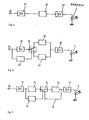
- the input voltage U E present at the input of the circuit arrangement is amplified in a first amplifier 41 and fed to a compensation stage 42, which is constructed in such a way that it transforms the current or voltage curve for the control of the LED in such a way that due to the thermal Behavior of the LED occurring distortions, such as overshoots, are compensated.
- the output signal of the compensation stage 42 can be amplified again by means of a second amplifier 43.
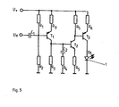
- FIG. 5 An exemplary embodiment for the compensation stage is shown in FIG. 5.
- the input voltage U reaches a connection capacitor C 1 at the connection point of two resistors R 1 and R 2 , which lie between the operating voltage U + and ground and serve as a voltage divider.
- the connection point of the resistors R 1 and R 2 is connected to the base of a pnp transistor T 1 .
- the emitter of this transistor T 1 is connected to the operating voltage source U via an emitter resistor R 3 , and the collector of this transistor T 1 is connected to ground via a collector resistor R 3 .
- This collector resistor R 3 is connected in parallel from a capacitor C 2 and a resistor R 4 .
- connection point between resistor R 3 and the collector of the first transistor T 1 is connected to the base of a second transistor T2 of the npn type, the collector of which is connected to the operating voltage source U + via a collector resistor R 5 , and the emitter of which is connected to ground via an emitter resistor R 7 is present.
- the collector of the second transistor T 2 is connected to the base of a third transistor T 3 of the pnp type, the emitter of which is connected to the operating voltage source U + via an emitter resistor R 6 .
- the collector of the third transistor T 3 is connected to an LED 1, the cathode of which is grounded.
- This means that the signal with which the LED is driven is just transformed according to the invention in such a way that there is essentially an inversely proportional signal curve to the overshoot curve of the output signal of the LED 1.
- an LR link can also be used instead of an RC link.
- the LED drive voltage U E is fed, optionally via a first amplifier 61, both to a switching stage 62 and to a circuit stage 63, ie a differentiator 63, which differentiates between the rising and falling edges of the LED drive signal.
- the output signal of the differentiator 63 switches the switching stage 62 into the upper or lower switching state depending on whether a rising or a falling edge has been detected, so that the control signal U E either via a compensator stage 64 or via a compensator stage 65 - and, if appropriate reaches the LED 1 via a second amplifier 66.
- the differentiator 63 is designed such that it only provides an output signal for switching the switching stage 62 when edges with a certain minimum steepness occur. If the slope is below the minimum slope, there is no changeover between the compensation stages 64 and 65.
- the signal change is relatively slow, there is relatively enough time for a temperature equalization between the junction and the LED housing or the environment, so that overshoots or distortions due to a short-term change in the junction temperature do not or not noticeably distort the output signal of the LED .
- a further embodiment of the invention consists in combining the two separate compensation stages 64 and 65 shown schematically in FIG. 6 in a combination stage and, when using RC and / or LR elements for the signal shaping of the control signal for the LED, only within the single switching stage to switch between two time constant values 1 and Z 2 , for example by changing the capacitor, resistance and / or induction values when a rising or falling edge of the LED drive signal occurs.
- the circuit arrangement according to the invention can be further simplified and manufactured inexpensively.
- the control signal U E is fed - if necessary via a first amplifier 71 to a first compensation stage 72 and at the same time to a differentiator 73 which, depending on whether a rising or falling edge occurs, switches over a switching stage 74 which is connected after the first compensation stage 72.
- An output of the switching stage 74 is connected to a second compensation stage 75 and at the second output of the switching stage 74 there is a bypass line 76 with which the second compensation stage 75 can be bypassed or rendered ineffective.
- the output signal of the second compensation stage 75 or the first compensation stage 72 with an effective bypass line 76 reaches the LED 1, possibly via a second amplifier.
- the time constants for the distortions differ with regard to the rising and falling edge of the control signal.
- a compensation stage therefore, either the distortion occurring on the rising edge or the distortion occurring on the falling edge can be completely compensated, and a certain residual distortion remains from the respective other distortion.
- This residual distortion can be compensated for by an additional compensation stage, which is activated for the edge for which residual distortion remains.
- This additional compensation stage is the second compensation stage 75 shown in FIG. 7, which is activated by the differentiator 73 and the switching stage 74 each time the edge occurs, which has not yet been fully compensated.
Landscapes
- Physics & Mathematics (AREA)
- Electromagnetism (AREA)
- Engineering & Computer Science (AREA)
- Computer Networks & Wireless Communication (AREA)
- Signal Processing (AREA)
- Nonlinear Science (AREA)
- Led Devices (AREA)
Applications Claiming Priority (2)
| Application Number | Priority Date | Filing Date | Title |
|---|---|---|---|
| DE19853519711 DE3519711A1 (de) | 1985-06-01 | 1985-06-01 | Schaltungsanordnung zur ansteuerung einer lichtemittierenden diode |
| DE3519711 | 1985-06-01 |
Publications (3)
| Publication Number | Publication Date |
|---|---|
| EP0207274A2 true EP0207274A2 (fr) | 1987-01-07 |
| EP0207274A3 EP0207274A3 (en) | 1989-04-12 |
| EP0207274B1 EP0207274B1 (fr) | 1993-01-07 |
Family
ID=6272214
Family Applications (1)
| Application Number | Title | Priority Date | Filing Date |
|---|---|---|---|
| EP86106886A Expired - Lifetime EP0207274B1 (fr) | 1985-06-01 | 1986-05-21 | Circuit d'attaque pour diode émettrice de lumière |
Country Status (4)
| Country | Link |
|---|---|
| US (1) | US4771219A (fr) |
| EP (1) | EP0207274B1 (fr) |
| DE (2) | DE3519711A1 (fr) |
| DK (1) | DK164680C (fr) |
Cited By (1)
| Publication number | Priority date | Publication date | Assignee | Title |
|---|---|---|---|---|
| WO2011003393A1 (fr) * | 2009-07-09 | 2011-01-13 | Jacobs University Bremen Ggmbh | Dispositif émetteur pour une transmission optique de données avec une source lumineuse non linéaire et dispositif récepteur associé |
Families Citing this family (4)
| Publication number | Priority date | Publication date | Assignee | Title |
|---|---|---|---|---|
| US5825399A (en) * | 1996-02-28 | 1998-10-20 | Eastman Kodak Company | Data-dependent thermal compensation for an LED printhead |
| US5929568A (en) * | 1997-07-08 | 1999-07-27 | Korry Electronics Co. | Incandescent bulb luminance matching LED circuit |
| NL1033688C2 (nl) * | 2007-04-13 | 2008-10-14 | Omron Europ B V | Werkwijze en inrichting voor het omzetten van een ingangsspanning naar een galvanisch gescheiden uitgangssignaal. |
| US11784637B1 (en) * | 2022-05-10 | 2023-10-10 | Cambridge Gan Devices Limited | Edge detection circuit |
Family Cites Families (6)
| Publication number | Priority date | Publication date | Assignee | Title |
|---|---|---|---|---|
| US3705316A (en) * | 1971-12-27 | 1972-12-05 | Nasa | Temperature compensated light source using a light emitting diode |
| JPS5851435B2 (ja) * | 1976-05-25 | 1983-11-16 | 富士通株式会社 | 発光素子の駆動方式 |
| US4160934A (en) * | 1977-08-11 | 1979-07-10 | Bell Telephone Laboratories, Incorporated | Current control circuit for light emitting diode |
| FR2415332A1 (fr) * | 1978-01-20 | 1979-08-17 | Thomson Csf | Dispositif d'alimentation de source lumineuse a semi-conducteur |
| US4182977A (en) * | 1978-06-01 | 1980-01-08 | Trw Inc. | Constant output light emitting device |
| FR2495412A1 (fr) * | 1980-12-02 | 1982-06-04 | Thomson Csf | Systeme de transmission d'informations a modulation directe de la lumiere a liaison optique a bande passante etendue vers les frequences basses et le continu |
-
1985
- 1985-06-01 DE DE19853519711 patent/DE3519711A1/de active Granted
-
1986
- 1986-05-21 DE DE8686106886T patent/DE3687433D1/de not_active Expired - Fee Related
- 1986-05-21 EP EP86106886A patent/EP0207274B1/fr not_active Expired - Lifetime
- 1986-05-30 DK DK254186A patent/DK164680C/da active
- 1986-06-02 US US06/869,709 patent/US4771219A/en not_active Expired - Fee Related
Cited By (1)
| Publication number | Priority date | Publication date | Assignee | Title |
|---|---|---|---|---|
| WO2011003393A1 (fr) * | 2009-07-09 | 2011-01-13 | Jacobs University Bremen Ggmbh | Dispositif émetteur pour une transmission optique de données avec une source lumineuse non linéaire et dispositif récepteur associé |
Also Published As
| Publication number | Publication date |
|---|---|
| DE3687433D1 (de) | 1993-02-18 |
| DK164680B (da) | 1992-07-27 |
| EP0207274B1 (fr) | 1993-01-07 |
| US4771219A (en) | 1988-09-13 |
| DK254186A (da) | 1986-12-02 |
| DE3519711A1 (de) | 1986-12-04 |
| DE3519711C2 (fr) | 1988-10-20 |
| DK254186D0 (da) | 1986-05-30 |
| EP0207274A3 (en) | 1989-04-12 |
| DK164680C (da) | 1992-12-14 |
Similar Documents
| Publication | Publication Date | Title |
|---|---|---|
| DE69225589T2 (de) | Vorverstärker | |
| EP0207274B1 (fr) | Circuit d'attaque pour diode émettrice de lumière | |
| DE2249859B2 (de) | Integrierte Verstärkerschalung | |
| DE1292200B (de) | Verfahren zur Temperaturkompensation von Thermistoren bei der pilotgesteuerten Pegelregelung von UEbertragungssystemen | |
| DE2749767C3 (de) | Schaltungsanordnung zur Helligkeitssteuerung von Leuchtdioden in Leuchtdiodenfeldern | |
| DE4138661C1 (fr) | ||
| DE2660031B1 (de) | Digitale Anzeigeschaltung fuer einen fotografischen Belichtungsmesser | |
| DE1538714A1 (de) | Steuersystem fuer Elektromotoren | |
| DE2731666C3 (de) | Anordnung zum Konstanthalten der Drehzahl eines rotierenden Elements, insbesondere eines Plattentellers eines Plattenspielers | |
| DE2167102C2 (de) | Vorrichtung zum Regeln der Lichtmenge | |
| DE8904733U1 (de) | Heißluftpistole | |
| DE2728713A1 (de) | Elektronischer witterungsabhaengiger heizungsregler | |
| EP0410188A2 (fr) | Montage pour la protection d'un commutateur rythmé à semi-conducteur | |
| DE709138C (de) | Schaltung zur Amplitudenregelung, insbesondere zur selbsttaetigen Regelung der Eingangsspannung von Verstaerkern | |
| DE1156110B (de) | Regelschaltung fuer einen Verstaerker | |
| DE3520691A1 (de) | Verfahren und schaltungsanordnung zur beruehrungsfreien temperaturmessung | |
| DE2047755B2 (de) | Einrichtung zur selbsstaetigen verstaerkungsregelung fuer einen verstaerker, insbesondere transistor verstaerker, in hochfrequenzspannungen fuehrenden kabelnetzen | |
| DE3150871A1 (de) | "steuereinrichtung fuer eine, durch einen magneten gesteuerte einrichtung" | |
| EP0296307A1 (fr) | Circuit pour régulateur analogue electronique | |
| DE2641535A1 (de) | Spannungsteiler mit steuerbarem teilerverhaeltnis | |
| DE2811030A1 (de) | Schaltungsanordnung zur speisung von lumineszenz-dioden | |
| CH683291A5 (de) | Verfahren und Schaltungsanordnung zur Vermeidung von Abbildungsfehlern in Wärmebildgeräten. | |
| DE3940345A1 (de) | Lediglich zwei anschlussleitungen aufweisende schaltung fuer einen auf eine veraenderung magnetischer feldlinien ansprechenden sensor und magnetfeldsensor mit einer derartigen schaltung | |
| EP0354462A2 (fr) | Agencement de circuit pour détecteurs d'infrarouge | |
| DE2018534C3 (de) | Belichtungsautomatik für eine Kamera |
Legal Events
| Date | Code | Title | Description |
|---|---|---|---|
| PUAI | Public reference made under article 153(3) epc to a published international application that has entered the european phase |
Free format text: ORIGINAL CODE: 0009012 |
|
| AK | Designated contracting states |
Kind code of ref document: A2 Designated state(s): BE DE FR GB IT NL SE |
|
| PUAL | Search report despatched |
Free format text: ORIGINAL CODE: 0009013 |
|
| AK | Designated contracting states |
Kind code of ref document: A3 Designated state(s): BE DE FR GB IT NL SE |
|
| 17P | Request for examination filed |
Effective date: 19890510 |
|
| RAP1 | Party data changed (applicant data changed or rights of an application transferred) |
Owner name: RICHARD HIRSCHMANN GMBH & CO. |
|
| 17Q | First examination report despatched |
Effective date: 19910517 |
|
| GRAA | (expected) grant |
Free format text: ORIGINAL CODE: 0009210 |
|
| AK | Designated contracting states |
Kind code of ref document: B1 Designated state(s): BE DE FR GB IT NL SE |
|
| REF | Corresponds to: |
Ref document number: 3687433 Country of ref document: DE Date of ref document: 19930218 |
|
| PGFP | Annual fee paid to national office [announced via postgrant information from national office to epo] |
Ref country code: SE Payment date: 19930225 Year of fee payment: 8 |
|
| ITF | It: translation for a ep patent filed | ||
| PGFP | Annual fee paid to national office [announced via postgrant information from national office to epo] |
Ref country code: FR Payment date: 19930331 Year of fee payment: 8 |
|
| GBT | Gb: translation of ep patent filed (gb section 77(6)(a)/1977) |
Effective date: 19930330 |
|
| PGFP | Annual fee paid to national office [announced via postgrant information from national office to epo] |
Ref country code: GB Payment date: 19930507 Year of fee payment: 8 |
|
| ET | Fr: translation filed | ||
| PGFP | Annual fee paid to national office [announced via postgrant information from national office to epo] |
Ref country code: BE Payment date: 19930517 Year of fee payment: 8 |
|
| PGFP | Annual fee paid to national office [announced via postgrant information from national office to epo] |
Ref country code: NL Payment date: 19930531 Year of fee payment: 8 |
|
| PGFP | Annual fee paid to national office [announced via postgrant information from national office to epo] |
Ref country code: DE Payment date: 19930713 Year of fee payment: 8 |
|
| PLBE | No opposition filed within time limit |
Free format text: ORIGINAL CODE: 0009261 |
|
| STAA | Information on the status of an ep patent application or granted ep patent |
Free format text: STATUS: NO OPPOSITION FILED WITHIN TIME LIMIT |
|
| 26N | No opposition filed | ||
| PG25 | Lapsed in a contracting state [announced via postgrant information from national office to epo] |
Ref country code: GB Effective date: 19940521 |
|
| PG25 | Lapsed in a contracting state [announced via postgrant information from national office to epo] |
Ref country code: SE Effective date: 19940522 |
|
| PG25 | Lapsed in a contracting state [announced via postgrant information from national office to epo] |
Ref country code: BE Effective date: 19940531 |
|
| BERE | Be: lapsed |
Owner name: RICHARD HIRSCHMANN G.M.B.H. & CO. Effective date: 19940531 |
|
| PG25 | Lapsed in a contracting state [announced via postgrant information from national office to epo] |
Ref country code: NL Effective date: 19941201 |
|
| NLV4 | Nl: lapsed or anulled due to non-payment of the annual fee | ||
| GBPC | Gb: european patent ceased through non-payment of renewal fee |
Effective date: 19940521 |
|
| EUG | Se: european patent has lapsed |
Ref document number: 86106886.4 Effective date: 19941210 |
|
| PG25 | Lapsed in a contracting state [announced via postgrant information from national office to epo] |
Ref country code: FR Effective date: 19950131 |
|
| PG25 | Lapsed in a contracting state [announced via postgrant information from national office to epo] |
Ref country code: DE Effective date: 19950201 |
|
| EUG | Se: european patent has lapsed |
Ref document number: 86106886.4 |
|
| REG | Reference to a national code |
Ref country code: FR Ref legal event code: ST |
|
| PG25 | Lapsed in a contracting state [announced via postgrant information from national office to epo] |
Ref country code: IT Free format text: LAPSE BECAUSE OF NON-PAYMENT OF DUE FEES;WARNING: LAPSES OF ITALIAN PATENTS WITH EFFECTIVE DATE BEFORE 2007 MAY HAVE OCCURRED AT ANY TIME BEFORE 2007. THE CORRECT EFFECTIVE DATE MAY BE DIFFERENT FROM THE ONE RECORDED. Effective date: 20050521 |