EP0207650B1 - Elektronischer Oszillator mit grossem Bereich - Google Patents
Elektronischer Oszillator mit grossem Bereich Download PDFInfo
- Publication number
- EP0207650B1 EP0207650B1 EP86304343A EP86304343A EP0207650B1 EP 0207650 B1 EP0207650 B1 EP 0207650B1 EP 86304343 A EP86304343 A EP 86304343A EP 86304343 A EP86304343 A EP 86304343A EP 0207650 B1 EP0207650 B1 EP 0207650B1
- Authority
- EP
- European Patent Office
- Prior art keywords
- oscillator
- impedance
- capacitor
- amplifier
- circuit
- Prior art date
- Legal status (The legal status is an assumption and is not a legal conclusion. Google has not performed a legal analysis and makes no representation as to the accuracy of the status listed.)
- Expired
Links
- 239000003990 capacitor Substances 0.000 claims abstract description 90
- 230000010355 oscillation Effects 0.000 claims description 21
- 230000003071 parasitic effect Effects 0.000 claims description 13
- 230000010363 phase shift Effects 0.000 claims description 12
- 230000008878 coupling Effects 0.000 claims description 9
- 238000010168 coupling process Methods 0.000 claims description 9
- 238000005859 coupling reaction Methods 0.000 claims description 9
- 230000005540 biological transmission Effects 0.000 claims description 6
- 230000000694 effects Effects 0.000 claims description 4
- 230000001419 dependent effect Effects 0.000 claims 1
- 238000010586 diagram Methods 0.000 description 7
- 230000004048 modification Effects 0.000 description 7
- 238000012986 modification Methods 0.000 description 7
- 230000009471 action Effects 0.000 description 4
- 239000013078 crystal Substances 0.000 description 3
- 230000008859 change Effects 0.000 description 2
- 238000001914 filtration Methods 0.000 description 2
- 230000002411 adverse Effects 0.000 description 1
- 230000003321 amplification Effects 0.000 description 1
- 230000003466 anti-cipated effect Effects 0.000 description 1
- 230000002238 attenuated effect Effects 0.000 description 1
- 230000000903 blocking effect Effects 0.000 description 1
- 239000004020 conductor Substances 0.000 description 1
- 230000036039 immunity Effects 0.000 description 1
- 238000004519 manufacturing process Methods 0.000 description 1
- 238000003199 nucleic acid amplification method Methods 0.000 description 1
- 230000009290 primary effect Effects 0.000 description 1
- 230000009467 reduction Effects 0.000 description 1
- 230000001172 regenerating effect Effects 0.000 description 1
- 230000002459 sustained effect Effects 0.000 description 1
- 230000007704 transition Effects 0.000 description 1
Images


Classifications
-
- H—ELECTRICITY
- H03—ELECTRONIC CIRCUITRY
- H03B—GENERATION OF OSCILLATIONS, DIRECTLY OR BY FREQUENCY-CHANGING, BY CIRCUITS EMPLOYING ACTIVE ELEMENTS WHICH OPERATE IN A NON-SWITCHING MANNER; GENERATION OF NOISE BY SUCH CIRCUITS
- H03B5/00—Generation of oscillations using amplifier with regenerative feedback from output to input
- H03B5/08—Generation of oscillations using amplifier with regenerative feedback from output to input with frequency-determining element comprising lumped inductance and capacitance
- H03B5/12—Generation of oscillations using amplifier with regenerative feedback from output to input with frequency-determining element comprising lumped inductance and capacitance active element in amplifier being semiconductor device
- H03B5/1231—Generation of oscillations using amplifier with regenerative feedback from output to input with frequency-determining element comprising lumped inductance and capacitance active element in amplifier being semiconductor device the amplifier comprising one or more bipolar transistors
-
- H—ELECTRICITY
- H03—ELECTRONIC CIRCUITRY
- H03B—GENERATION OF OSCILLATIONS, DIRECTLY OR BY FREQUENCY-CHANGING, BY CIRCUITS EMPLOYING ACTIVE ELEMENTS WHICH OPERATE IN A NON-SWITCHING MANNER; GENERATION OF NOISE BY SUCH CIRCUITS
- H03B5/00—Generation of oscillations using amplifier with regenerative feedback from output to input
- H03B5/08—Generation of oscillations using amplifier with regenerative feedback from output to input with frequency-determining element comprising lumped inductance and capacitance
- H03B5/12—Generation of oscillations using amplifier with regenerative feedback from output to input with frequency-determining element comprising lumped inductance and capacitance active element in amplifier being semiconductor device
- H03B5/1203—Generation of oscillations using amplifier with regenerative feedback from output to input with frequency-determining element comprising lumped inductance and capacitance active element in amplifier being semiconductor device the amplifier being a single transistor
-
- H—ELECTRICITY
- H03—ELECTRONIC CIRCUITRY
- H03B—GENERATION OF OSCILLATIONS, DIRECTLY OR BY FREQUENCY-CHANGING, BY CIRCUITS EMPLOYING ACTIVE ELEMENTS WHICH OPERATE IN A NON-SWITCHING MANNER; GENERATION OF NOISE BY SUCH CIRCUITS
- H03B5/00—Generation of oscillations using amplifier with regenerative feedback from output to input
- H03B5/08—Generation of oscillations using amplifier with regenerative feedback from output to input with frequency-determining element comprising lumped inductance and capacitance
- H03B5/12—Generation of oscillations using amplifier with regenerative feedback from output to input with frequency-determining element comprising lumped inductance and capacitance active element in amplifier being semiconductor device
- H03B5/1237—Generation of oscillations using amplifier with regenerative feedback from output to input with frequency-determining element comprising lumped inductance and capacitance active element in amplifier being semiconductor device comprising means for varying the frequency of the generator
- H03B5/124—Generation of oscillations using amplifier with regenerative feedback from output to input with frequency-determining element comprising lumped inductance and capacitance active element in amplifier being semiconductor device comprising means for varying the frequency of the generator the means comprising a voltage dependent capacitance
- H03B5/1243—Generation of oscillations using amplifier with regenerative feedback from output to input with frequency-determining element comprising lumped inductance and capacitance active element in amplifier being semiconductor device comprising means for varying the frequency of the generator the means comprising a voltage dependent capacitance the means comprising voltage variable capacitance diodes
-
- H—ELECTRICITY
- H03—ELECTRONIC CIRCUITRY
- H03B—GENERATION OF OSCILLATIONS, DIRECTLY OR BY FREQUENCY-CHANGING, BY CIRCUITS EMPLOYING ACTIVE ELEMENTS WHICH OPERATE IN A NON-SWITCHING MANNER; GENERATION OF NOISE BY SUCH CIRCUITS
- H03B2200/00—Indexing scheme relating to details of oscillators covered by H03B
- H03B2200/0002—Types of oscillators
- H03B2200/0006—Clapp oscillator
-
- H—ELECTRICITY
- H03—ELECTRONIC CIRCUITRY
- H03B—GENERATION OF OSCILLATIONS, DIRECTLY OR BY FREQUENCY-CHANGING, BY CIRCUITS EMPLOYING ACTIVE ELEMENTS WHICH OPERATE IN A NON-SWITCHING MANNER; GENERATION OF NOISE BY SUCH CIRCUITS
- H03B2200/00—Indexing scheme relating to details of oscillators covered by H03B
- H03B2200/0002—Types of oscillators
- H03B2200/0008—Colpitts oscillator
-
- H—ELECTRICITY
- H03—ELECTRONIC CIRCUITRY
- H03B—GENERATION OF OSCILLATIONS, DIRECTLY OR BY FREQUENCY-CHANGING, BY CIRCUITS EMPLOYING ACTIVE ELEMENTS WHICH OPERATE IN A NON-SWITCHING MANNER; GENERATION OF NOISE BY SUCH CIRCUITS
- H03B2200/00—Indexing scheme relating to details of oscillators covered by H03B
- H03B2200/003—Circuit elements of oscillators
- H03B2200/004—Circuit elements of oscillators including a variable capacitance, e.g. a varicap, a varactor or a variable capacitance of a diode or transistor
-
- H—ELECTRICITY
- H03—ELECTRONIC CIRCUITRY
- H03B—GENERATION OF OSCILLATIONS, DIRECTLY OR BY FREQUENCY-CHANGING, BY CIRCUITS EMPLOYING ACTIVE ELEMENTS WHICH OPERATE IN A NON-SWITCHING MANNER; GENERATION OF NOISE BY SUCH CIRCUITS
- H03B2200/00—Indexing scheme relating to details of oscillators covered by H03B
- H03B2200/006—Functional aspects of oscillators
- H03B2200/0088—Reduction of noise
-
- H—ELECTRICITY
- H03—ELECTRONIC CIRCUITRY
- H03B—GENERATION OF OSCILLATIONS, DIRECTLY OR BY FREQUENCY-CHANGING, BY CIRCUITS EMPLOYING ACTIVE ELEMENTS WHICH OPERATE IN A NON-SWITCHING MANNER; GENERATION OF NOISE BY SUCH CIRCUITS
- H03B2200/00—Indexing scheme relating to details of oscillators covered by H03B
- H03B2200/006—Functional aspects of oscillators
- H03B2200/0088—Reduction of noise
- H03B2200/009—Reduction of phase noise
-
- H—ELECTRICITY
- H03—ELECTRONIC CIRCUITRY
- H03B—GENERATION OF OSCILLATIONS, DIRECTLY OR BY FREQUENCY-CHANGING, BY CIRCUITS EMPLOYING ACTIVE ELEMENTS WHICH OPERATE IN A NON-SWITCHING MANNER; GENERATION OF NOISE BY SUCH CIRCUITS
- H03B2200/00—Indexing scheme relating to details of oscillators covered by H03B
- H03B2200/006—Functional aspects of oscillators
- H03B2200/0092—Measures to linearise or reduce distortion of oscillator characteristics
-
- H—ELECTRICITY
- H03—ELECTRONIC CIRCUITRY
- H03B—GENERATION OF OSCILLATIONS, DIRECTLY OR BY FREQUENCY-CHANGING, BY CIRCUITS EMPLOYING ACTIVE ELEMENTS WHICH OPERATE IN A NON-SWITCHING MANNER; GENERATION OF NOISE BY SUCH CIRCUITS
- H03B2201/00—Aspects of oscillators relating to varying the frequency of the oscillations
- H03B2201/02—Varying the frequency of the oscillations by electronic means
- H03B2201/0208—Varying the frequency of the oscillations by electronic means the means being an element with a variable capacitance, e.g. capacitance diode
Definitions
- This invention relates generally to electronic oscillators and more particularly to improvements in electronic oscillators of the Colpitts and/or Clapp type.
- the Colpitts and Clapp oscillators are well known for having good properties in the communications field.
- the tuning range at ultra high frequencies (above about 500 MHz) the tuning range, the tuning linearity, power output flatness, and noise performance become greatly degraded.
- the current state of the art has been to accept a limited tuning range and then use multiple oscillators to cover wide bands and to use filtered and amplified harmonics of lower frequency oscillators to achieve acceptable power flatness and phase noise performance.
- a wideband electronic oscillator comprising: a resonant tank circuit including an inductance means, a main capacitance and second and third capacitors connected in series with one another for producing oscillations; a signal amplifier for overcoming losses to sustain oscillations in the tank circuit, said amplifier having an input and an output, said amplifier amplifying a signal in a power output path and also providing a feedback signal from its output, which feedback signal is fed back to the input of the amplifier via part of the tank circuit which part includes one of said second and third capacitors; a first impedance connected between said output and ground; a second impedance connected from a point between said second and third capacitors to said output; characterised in that: said second impedance includes a reactance for maintaining the phase shift of the feedback signal between the input and output of said amplifier at substantially zero degrees and for reducing noise components near the oscillating frequency, said second impedance having a high value at low frequencies in relation to the first impedance so that the low frequency noise components are
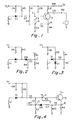
- an oscillator which includes a series resonant tuned tank circuit comprised of a main resonating inductor L1, a main tuning capacitor C1, shown as a varactor diode, a DC blocking capacitor C2, and feedback signal divider capacitors C3 and C4 connected in series.
- Capacitor C2 is not essential when C1 is a varactor diode but its use, connected as shown, is preferred.
- the side of the inductor L1 opposite its connection to capacitor C1 is shown connected to ground.
- the side of the divider capacitor C4 opposite its connection to capacitor C3 is shown connected to ground.
- Inductor L1 which serves as the inductance means for the tank circuit, may be a variable inductor used to change the resonant frequency of the tank circuit.
- capacitor C1 would be a fixed value and preferably there would be no C2.
- the inductance means may also be a tuned cavity or crystal resonator. A crystal resonator would provide similar results except for the wider tuning range. However, the tuning range would be wide as compared with other crystal oscillators.
- a DC voltage tuning input terminal VT is connected through a resistor R5 to tuning capacitor C1 to bias capacitor C1. More specifically, terminal VT supplies a positive tuning voltage at the cathode electrode with respect to the anode electrode of varactor diode C1. Resistor R5 is of a high value so as not to load the Q of the tank circuit. Resistor R5 may be an RF choke, a high impedance active device such as a transistor, or another network presenting a high RF impedance and a controlled DC resistance.
- An RF bypass capacitor C6 is connected to input terminal VT and to ground to provide a low pass filter and thereby short out any RF signals.
- Capacitor C6 is a low reactance at minimum oscillator frequencies and a high reactance at maximum anticipated modulation frequencies.
- the feedback loop for sustaining the oscillations in the tank circuit includes feedback signal dividing capacitor C3, an amplifier A, and an impedance in the form of a capacitor C5 connected to point D between capacitors C3 and C4 and to the feedback output of the amplifier A at point E.
- Amplifier A as shown is an active device and specifically is an NPN transistor having the base and emitter electrodes connected in the feedback loop. Other active devices such as a FET or a vacuum tube may be used in place of a transistor.
- the prior art Colpitts oscillator has a direct connection or short where capacitor C5 is connected which results in a less desirable performance, as is discussed more fully hereinafter.
- a feedback output impedance in the form of a resistor R4 is shown connected between the transistor emitter which is the feedback output of the amplifier, designated point E, and ground.
- Resistor R4 may be replaced with a choke, an output transformer, a filter or other network which looks like a high impedance at RF frequencies, and a controlled bias impedance to DC.
- a DC voltage supply terminal VS is connected through a resistor R3 and an inductor L2 to the collector electrode of the transistor to supply a DC feed voltage thereto.
- a resistor R1 is connected to inductor L2 and to the base of the transistor to connect resistor R1 and inductor L2 between the base and collector electrodes of the transistor.
- Resistor R2 is connected to the base of the transistor and to ground. In this way resistors R1 and R2 are selected to provide the proper DC bias for the transistor and are selected to have a sufficiently large value so as not to degrade the Q of the tuned circuit.
- Resistors R1 and R2 may be replaced with other networks such as chokes or may be absent as required to provide the proper bias conditions for the transistor.
- the power output is shown as being taken from the collector of the transistor.
- An AC output coupling and impedance matching arrangement is connected to the collector of the transistor and to a power output terminal PO which includes a capacitor C9 between the collector and power output terminal PO, inductor L2 coupled to the collector, and an RF bypass capacitor C8 connected to the inductor L2, resistor R1 and resistor R3 and ground to provide an RF ground.
- the output coupling and impedance matching can be accomplished in a number of ways which include changing L2 to a choke, resistor, filter, or other network which matches the active device to the desired output load.
- a load L is shown connected to the PO terminal. It is understood that the output power can be taken from other points in the circuit, as is discussed more fully hereinafter.
- the LC resonant tank circuit oscillates at a frequency C is the total capacitance in the tuned circuit.
- a portion of the feedback output of the amplifier A is applied in phase to the tank circuit and to the input of amplifier A to sustain oscillations.
- C2 In order not to reduce the effective value of C1, and thereby reduce tuning range, C2 should be much greater in value than C1. Values of C2 equal to ten to twenty times greater than a maximum value of C1 are typical. Capacitor C2 could be replaced by a conductor in applications where capacitor C1 is a mechanical DC isolated capacitor itself or, conversely, C1 is a fixed DC isolated value and inductor L1 is varied to change the resonant frequency of the oscillator.
- Capacitor C3 functions to provide a return path for the resonant circuit energy from point C to point D and provides a feedback path for feedback energy developed by the transistor from point D to point C.
- C3 must be chosen in conjunction with the rest of the tuned circuit capacitors to provide the proper voltage to ground which is the point C to ground tap point on the tuned circuit to insure that the transistor is commutated through a sufficient dynamic range to develop enough feedback voltage, at point E to ground, to sustain the criteria for oscillations over the entire intended tuning range of the oscillator. Values of C3 equal to two to ten times the value of capacitor C1 are typical.
- Capacitor C4 like capacitor C3, forms a return path for the resonant circuit from point D to ground.
- the value of C4 must be chosen in conjunction with the rest of the tuned circuit capacitors to provide the proper voltage to ground, which is the point C to ground tap point on the tuned circuit, to insure that the transistor is commutated through enough dynamic range to develop sufficient feedback voltage, at point E to ground, to sustain the criteria for oscillations over the entire intended tuning range of the oscillator. Values of C4 equal to two to ten times the value of capacitor C1 are typical.
- Capacitor C4 also functions as a part of the return path for energy generated at point E to ground. In this sense, it functions as an RF bypass and has a primary effect on transistor gain over the tuning range. Capacitor C4, along with capacitor C3, sets the tap point D to ground voltage on the tuned circuit and controls the amount of feedback voltage applied to point C from point D generated by the transistor at point E by its commutation through its dynamic range.
- the tuning range for the oscillator may be approximated by (a) neglecting all stray and interelectrode capacitances of the transistor, (b) neglecting all stray series resistances, inductances and capacitances, (c) neglecting all stray shunt circuit capacitances between elements and to ground.
- CT max (CTotal) in the series tuned circuit would calculate out to: CT max ⁇ .69 x C1 max Similarly, for values of C1 maximum ⁇ ⁇ C2, C3, C4 i.e., large capacitor tuning ratios) CT minimum ⁇ C1 minimum.
- the base to emitter capacitance in series with C4 can series resonate with stray interconnecting inductances to effectively short the transistor input to ground.
- parasitic resonances In addition, the ability of these parasitic resonances to cause undesired circuit operation is not simply traceable to pure shorting or open conditions. For example, parasitic resonances, well out of the oscillator intended tuning band, are seen to adversely affect proper operation. This condition results from disadvantageous phase shifts applied to the normal voltages and currents flowing in the transistor circuit. This is due to the transfer phase characteristics of the parasitic resonant circuits. For example, a positive voltage applied to the transistor base at point C is assumed to produce a corresponding voltage at point E minus a small base to emitter voltage drop in the transistor. This emitter voltage should be in phase with applied base voltage to produce proper transistor power amplification and feedback action.
- the voltage developed at point E may experience a phase shift due to the parasitic LRC circuits and thus not be applied to the feedback path in the proper phase to cause positive feedback. Hence, it will not sustain the desired regenerative buildup of oscillations.
- the main tuned circuit by definition allows the current flow and voltage to be precisely in phase only near the oscillation frequency. Since the transistor base currents and voltages are applied in phase to the base only at the normal frequency of resonance, then the voltage and current developed at point E (the emitter) must remain of equal phases in order that feedback voltage from point E to the base via the dividing capacitors C3 and C4 is itself in phase with the original base input signal and, hence, positive feedback.
- the emitter circuit forms a part of a parasitic tuned circuit at an entirely different (higher) frequency
- the voltage and current at the desired resonance frequency are now of differing phase and, when applied to point C through the capacitor C3, do not constitute a positive feedback signal at the proper resonant frequency within the bandwidth of the tuned circuit, and oscillations cease, as previously outlined.
- the present invention overcomes the above shortcomings of the Colpitts oscillator by introduction of an additional impedance in the path between point E and the feedback divider capacitors at point D.
- capacitors C3 and C4 are selected to optimize tuning range (as large as possible) consistent with proper impedance match to the input of the transistor, independently of their effect of causing troublesome parasitic resonance or parasitic phase shift effects on the emitter and feedback voltages and currents, as earlier discussed.
- the reactance network represented by capacitor C5 from point E to point D is selected to yield proper gain of the transistor, feedback amplitude and phase shift characteristics to the feedback energy independently of the values of C3 and C4 previously optimized as outlined.
- noise components near the oscillating frequency are reduced in amplitude in the feedback path by virtue of the voltage drop across C5 from point E to point D.
- the voltage divider consisting of capacitors C5 and C4 to ground, C4 was chosen, as above discussed, to have a larger value than allowed in the Colpitts oscillator. This improves the reduction in noise components. Improvements in near-in phase noise of six to ten decibels have been measured in a circuit according to the present invention, compared to the Colpitts oscillator.
- low frequency noise components are filtered to ground by being partially dissipated in resistor R4 by virtue of capacitor C5 in conjunction with resistor R4, providing a low pass filtering action.
- Low frequency noise energy which appears at point E, is presented with a very high impedance to the feedback path through capacitor C5 and a much lower impedance to ground through resistor R4.
- low frequency noise is effectively filtered in the circuit of the present invention from the feedback path by a greater amount than in the Colpitts oscillator where the low frequency noise is presented directly to point D in the tuned circuit.
- the modified oscillator shown in Figure 2 has another varactor diode C10 connected in series with varactor diode C1 with the cathodes of the two connected together.
- a DC return resistor R6 is connected to the anode of varactor diode C10. This circuit tends to reduce the harmonic generation in the varactor diodes.
- a varactor diode C11 is connected in series with varactor diode C1 with the cathodes of the two connected together.
- the anode of varactor diode C11 is connected to ground.
- the tuned circuit functions in a parallel resonant mode, C1 together with C11 being the main tuning capacitors and C2 simply coupling energy to the transistor.
- the high end of the band C11 is much less than the capacitance of the rest of the circuit and the circuit transitions to a series resonant circuit where C1 is now the main resonant capacitor and the overall oscillator tuning range is increased.
- the modified circuit shown in Figure 4 includes a tuned series resonant circuit that is tuned and ganged to the resonant tank circuit.
- This circuit consists of an inductor L3 and a varactor diode C12 connected between capacitor C5 and point D, together with a choke RFC connected between capacitor C5 and ground.
- An additional resistor R7 is added between point D and terminal VT.
- the value of resistor R5 is typically equal to the value of resistor R7 and the capacitance of capacitor C1 is equal to the capacitance of capacitor C12.
- This circuit is ganged to and adjusted to track the resonant frequency of the tuned circuit.
- This added tuned circuit filters the feedback signal, that is, it only allows the transistor to have maximum gain at the fundamental oscillator frequency and thereby functions as a tuned bandpass feedback filter. In this way harmonics and out-of-band noise are effectively attenuated in the oscillator output relative to the desired oscillator frequency. Since the current and voltage are in phase in a series resonant circuit at resonance, this tuned circuit, when properly aligned has no effect on the transfer phase of the circuit from point D to point E.
- a capacitor may be connected across resistor R4, as is described in Figure 5, but this is optional for the circuit of Figure 4.
- the added capacitor would improve the Q of the main tuned circuit by effectively shunting the value of R4 with a relatively lossless element.
- Other alternative impedance networks which could be connected between points D and E include a series RC network, a parallel RC network and a transformer network with the transformer primary and a capacitor connected in series between points D and E and the output PO taken from the transformer secondary.
- the modified circuit shown in Figure 5 has a capacitor C7 connected across resistor R4. This addition of C7 allows the adjustment of the transistor gain independently from the adjustment of the feedback impedance. Further, C7 changes the Q loading on the tuned circuit to the extent that there are improved stability and a higher performance that come with an associated higher Q value for the tuned circuit. Improvements in a loaded Q of a ratio of 2:1 have been realized as compared with that of the Colpitts oscillator.
- a further modification for Figure 5 would be to add an inductor between point E and resistor R4 which would improve low frequency noise immunity.
- This inductor may be chosen to look like a high impedance over the oscillator band and a low reactance at low frequencies.
- Capacitor C7 may be chosen to look like a high reactance at low noise frequencies. This circuit would short out feedback to the tuned circuit and transistor of low frequency noise and thus prevent such noise from appearing amplified in the output as AM noise or FM modulation of the output.
- a further modification shown in Figure 6 would be to add a capacitor C13 in the feedback loop between the base of the transistor and point C. This added capacitor would similarly be used to maintain proper impedance matching and proper phase relationships.
- FIG. 7 there is shown a transmission line section TL1 in place of inductor L1, a transmission line section TL2 in place of capacitor C4, and a transmission line section TL3 connected to resistor R4, together with a transmission line section TL4 in place of L2.
- This circuit would operate in the high microwave frequency range.
- An alternative power output circuit shown in Figure 8, has the power output terminal coupled to resistor R4 through a coupling capacitor C14.
- the coupling shown includes an amplifier circuit which, as shown, is an emitter follower circuit having a transistor T with its base coupled to inductor L1 through capacitor C15.
- a bias resistor R11 is connected between the base of the transistor and the VS terminal.
- a bias resistor R12 is connected between the base and ground.
- Resistor R13 is connected between the emitter and ground.
- An RF bypass capacitor C16 is connected to resistor R11 and terminal VS.
- a coupling capacitor C17 is connected between the emitter and output terminal PO.
- the load L is shown connected across output terminal PO.
Landscapes
- Inductance-Capacitance Distribution Constants And Capacitance-Resistance Oscillators (AREA)
- Burglar Alarm Systems (AREA)
- Glass Compositions (AREA)
- Oscillators With Electromechanical Resonators (AREA)
- Amplifiers (AREA)
Claims (24)
- Elektronischer Breitband-Oszillator, umfassend:
einen Resonanz-Abstimmungskreis mit einer Induktanz (L1), einer Hauptkapazität (C1) und einem zweiten und dritten Kondensator (C3 und C4), hintereinandergeschaltet zur Schwingungserzeugung.
einen Signalverstärker (A) für den Verlustausgleich zur Aufrechterhaltung von Schwingungen in dem Abstimmungskreis, welcher Verstärker einen Eingang und einen Ausgang besitzt und ein Signal in einem Leistungsausgangspfad verstärkt und außerdem ein Rückkopplungssignal von seinem Ausgang abgibt, welches Rückkopplungssignal an den Eingang des Verstärkers über einen Teil des Abstimmungskreises zurückgeleitet wird, welcher Teil entweder den genannten ersten oder den genannten zweiten Kondensator (C3,C4) enthält,
eine erste Impedanz (R4), die zwischen dem genannten Ausgang und Erde liegt,
eine zweite Impedanz, die zwischen einen Punkt zwischen dem genannten zweiten und dem genannten dritten Kondensator und den genannten Ausgang geschaltet ist, dadurch gekennzeichnet,
daß die genannte zweite Impedanz eine Reaktanz (C5) enthält, um die Phasenverschiebung des Rückkopplungssignals zwischen dem Eingang und dem Ausgang des genannten Verstärkers (A) auf im wesentlichen 0° zu halten, und um Rauschanteile in der Nähe der Schwingfrequenz herabzusetzen, welche zweite Impedanz (C5) bei niedrigen Frequenzen einen hohen Wert im Vergleich zu der ersten Impedanz (R4) hat, so daß die niederfrequenten Rauschanteile in der genannten ersten Impedanz (R4) abgeleitet werden, welche genannte zweite Impedanz (C5) ferner die Belastung der genannten ersten Impedanz auf den genannten Abstimmungskreis herabsetzt, um den Gütefaktor zu erhöhen und dadurch die Stabilität der Schwingungen in dem genannten Abstimmungskreis zu - Oszillator nach Anspruch 1, worin die genannte zweite Impedanz eine Kapazität (C5) umfaßt.
- Oszillator nach Anspruch 1 oder 2, worin die genannte Hauptkapazität einen Abstimmkondensator umfaßt.
- Oszillator nach Anspruch 3, worin die genannte Hauptkapazität eine Varaktordiode umfaßt.
- Oszillator nach Anspruch 4, umfassend eine Spannungsabstimmeingangsklemme zum Zuführen einer positiven Abstimmspannung auf eine Kathodenelektrode der genannten Varaktordiode, bezogen auf eine Anodenelektrode der genannten Varaktordiode.
- Qszillator nach einem der vorhergehenden Ansprüche, worin der genannte Verstärker eine aktive Vorrichtung in Form eines Transistors ist, dessen Basis und Emitter in der genennte Rückkopplungsschleife liegen.
- Oszillator nach Anspruch 6, worin die genannte Basis mit der genannten Hauptkapazität und mit dem genannten einen Kondensator der genannten zweiten und dritten Kondensatoren verbunden ist.
- Oszillator nach Anspruch 6 oder 7, worin der genannte Emitter mit der genannten ersten Impedanz verbunden ist.
- Oszillator nach einem der vorhergehenden Ansprüche, worin die genannte erste Impedanz ein Widerstand ist.
- Oszillator nach einem der vorhergehenden Ansprüche, worin die Kapazität der genannten Kondensatoren in dem genannten Resonanz-Abstimmungskreis, ausgenommen die genannte Hauptkapazität, verhältnismäßig groß im Vergleich zu dar Kapazität der genannten Hauptkapazität ist, so daß die Resonanzfrequenz des Abstimmungskreises in erster Linie von dem Wert der genannten Hauptkepazität abhängt.
- Oszillator nach Anspruch 10, worin der genannte Resonanzfrequenzabstimmbereich ein Verhältnis von mehr als 3:1 hat.
- Oszillator nach einem der vorhergehenden Ansprüche, worin der Wert der genannten zweiten Impedanz im Vergleich zu dem Kapazitätswert des anderen Kondensators der genannten beiden zweiten und dritten Kondensatoren so gewählt ist, daß die Wirkungen von störender Phasenverschiebung und störender Resonanz auf des Rückkopplungssignal so gering wie möglich bleiben.
- Oszillator nach einem der vorhergehenden Ansprüche, worin die genannte zweite Impedanz das Einstellen des Gewinns des genannten Verstärkers unabhängig von der Kapazität des zweiten und dritten Kondensators ermöglicht, um über den Abstimmbereich eine verbesserte Ebenheit des Leistungsausgangs zu erzielen.
- Oszillator nach einem der vorhergehenden Ansprüche, worin die genannte Hauptkapazität eine erste Veraktordiode und eine zweite Varaktordiode umfaßt, die hintereinandergeschaltet sind, wobei die Kathoden der genannten Varakterdioden miteinander verbunden sind und ein Gleichstrom-Rückleitungswiderstand an die Anode der genannten zweiten Varaktordiode und an Erde gelegt ist.
- Oszilllator nach einem der Ansprüche 1 bis 13, worin die genannte Hauptkapazität eine erste Varaktordiode und eine zweite Varakterdiode umfaßt, die hintereinandergeschaltet sind, wobei die Kathoden der Verakterdioden miteinander verbunden sind und die Anode der zweiten Varakterdiode an Erde gelegt ist, um den Abstimmbereich zu erweitern.
- Oszillator nach einem der vorhergehenden Ansprüche, umfassend einen abgestimmten Reihenresonanzkreis, abgestimmt und gekuppelt mit dem genannten Resonanz-Abstimmungskreis, welcher abgestimmte Reihenresonanzkreis zwischen die genannte zweite Impedanz und die genannten zweiten und dritten Kondensatoren geschaltet ist.
- Oszillator nach einem der vorhergehenden Ansprüche, umfassend einen zu der genannten ersten Impedanz parallel geschaltetan Kondensator, um den Gewinn des genannten Verstärkers unabhängig von der Einstellung der genannten zweiten Impedanz einstellen zu können.
- Oszillator nach einem der vorhergehenden Ansprüche, umfassend einen Kondensator, der zwischen den genannten Eingang und den genannten einen Kondensator in der genannten Rückkopplungeschleife geschaltet ist.
- Oszillator nach einem der vorhergehenden Ansprüche, worin die genannte Induktivität, der andere der beiden zweiten und dritten Kondensatoren, ein mit der genannten zweiten Impedanz und der genannten ersten Impedenz verbundenes Element und ein zweites Element in dem Leistungsausgang das genannten Verstärkers Übertregungsleitungsabschnitte sind, die mit hohen Mikrowellenfrequenzen arbeiten.
- Oszillator nach einem der vorhergehenden Ansprüche, umfassend eine Leistungsausgangsklemme, gekoppelt über eine Wechselstrom-Auskopplungs- und Impedanzanpassungseinrichtung die mit einem Leistungsausgang des genannten Signalverstärkers verbunden ist.
- Oszillator nach Anspruch 20, worin die genannte Kopplungs- und Anpassungseinrichtung einen Kondensator umfaßt, der zwischen den genannten Verstärker und die genannte Leistungsausgangsklemme geschaltet ist, eine Induktivität, die an den genannten Kondensator und den genannten Verstärkerleistungsausgang gekoppelt ist, und einen Ableitkondensator, der zwischen die genannte Induktivität und Erde geschaltet ist, um eine HF-Erdung herzustellen.
- Oszillator nach einem der Ansprüche 1 bis 18, mit einer an die genannte erste Impedanz angeschlossenen Leistungsausgangsklemme.
- Oszillator nach einem der Ansprüche 1 bis 19, mit einer an die genannte Induktivität angeschlossenen Leistungsausgangsklemme.
- Oszillator nach Anspruch 23, mit einem Kopplungskondensator und einer aktiven Vorrichtung, geschaltet in einen Verstärkerkreis, der zwischen die genannte Leistungsausgangsklemme und die genannte Induktivität geschaltet ist.
Priority Applications (1)
| Application Number | Priority Date | Filing Date | Title |
|---|---|---|---|
| AT86304343T ATE73270T1 (de) | 1985-06-07 | 1986-06-06 | Elektronischer oszillator mit grossem bereich. |
Applications Claiming Priority (2)
| Application Number | Priority Date | Filing Date | Title |
|---|---|---|---|
| US742194 | 1985-06-07 | ||
| US06/742,194 US4621241A (en) | 1985-06-07 | 1985-06-07 | Wide range electronic oscillator |
Publications (3)
| Publication Number | Publication Date |
|---|---|
| EP0207650A2 EP0207650A2 (de) | 1987-01-07 |
| EP0207650A3 EP0207650A3 (en) | 1988-08-03 |
| EP0207650B1 true EP0207650B1 (de) | 1992-03-04 |
Family
ID=24983852
Family Applications (1)
| Application Number | Title | Priority Date | Filing Date |
|---|---|---|---|
| EP86304343A Expired EP0207650B1 (de) | 1985-06-07 | 1986-06-06 | Elektronischer Oszillator mit grossem Bereich |
Country Status (7)
| Country | Link |
|---|---|
| US (1) | US4621241A (de) |
| EP (1) | EP0207650B1 (de) |
| JP (1) | JPS61283202A (de) |
| AT (1) | ATE73270T1 (de) |
| CA (1) | CA1267941A (de) |
| DE (1) | DE3684045D1 (de) |
| HK (1) | HK82195A (de) |
Families Citing this family (39)
| Publication number | Priority date | Publication date | Assignee | Title |
|---|---|---|---|---|
| DE3730773A1 (de) * | 1987-09-12 | 1989-03-23 | Philips Patentverwaltung | Hochfrequenz-generator |
| US5053726A (en) * | 1990-04-10 | 1991-10-01 | Thomson Consumer Electronics, Inc. | Circuit for preventing VCXO mode jumping |
| JPH0492505A (ja) * | 1990-08-07 | 1992-03-25 | Matsushita Electric Ind Co Ltd | 電圧制御発振器 |
| US5138285A (en) * | 1991-07-19 | 1992-08-11 | Anadigics, Inc. | Method for reducing phase noise in oscillators |
| US5144264A (en) * | 1991-11-01 | 1992-09-01 | Motorola, Inc. | Wideband voltage controlled oscillator having open loop gain compensation |
| WO1994000912A1 (de) * | 1992-06-19 | 1994-01-06 | Deutsche Thomson-Brandt Gmbh | Oszillatorschaltung und deren verwendung |
| FI95522C (fi) * | 1992-11-27 | 1996-02-12 | Nokia Mobile Phones Ltd | Jänniteohjattu oskillaattori, jolla on laaja taajuusalue |
| US5525937A (en) * | 1992-12-28 | 1996-06-11 | Sony Corporation | Frequency conversion circuit with UHF/VHF common PLL buffer |
| FI97925C (fi) * | 1994-06-21 | 1997-03-10 | Nokia Mobile Phones Ltd | Virityslineaarisuudeltaan parannettu jänniteohjattu oskillaattori |
| US5473287A (en) * | 1994-11-14 | 1995-12-05 | Micronetics, Inc. | Electronic oscillator with transmission line tuning of phase noise and linearity |
| KR0153379B1 (ko) * | 1995-09-26 | 1998-11-16 | 김광호 | 디지탈 무선통신시스템의 업/다운컨버터용 전압제어발진기 |
| US5675478A (en) * | 1996-07-15 | 1997-10-07 | Vari-L Company, Inc. | Oscillator voltage regulator |
| US5856763A (en) * | 1997-03-05 | 1999-01-05 | Motorola Inc. | Dual frequency voltage controlled oscillator |
| GB2336492B (en) * | 1998-04-15 | 2000-06-07 | Motorola Gmbh | Voltage controlled oscillator |
| EP1097507A1 (de) * | 1998-07-20 | 2001-05-09 | Vari-L Company, Inc. | Oszillator mit energiesparmodus |
| US6181216B1 (en) * | 1999-07-19 | 2001-01-30 | General Instrument Corporation | Low phase-noise voltage controlled oscillator |
| EP1188227B1 (de) * | 2000-02-25 | 2007-07-25 | Infineon Technologies AG | Spannungsgesteuerter oszillator |
| US6504443B1 (en) | 2000-05-17 | 2003-01-07 | Nec America, Inc., | Common anode varactor tuned LC circuit |
| WO2002009269A1 (en) * | 2000-07-20 | 2002-01-31 | Paratek Microwave, Inc. | Voltage controlled oscillators including tunable dielectric devices |
| KR100759508B1 (ko) * | 2000-08-01 | 2007-09-18 | 정연문 | 귀환루프를 갖는 고주파 발진 회로 |
| US6462627B1 (en) * | 2000-08-25 | 2002-10-08 | Tropian Inc. | Oscillator circuit having reduced phase noise |
| US6466099B2 (en) | 2001-01-03 | 2002-10-15 | Motorola, Inc. | Voltage controlled oscillator (VCO) in colpitts configuration |
| US7180950B2 (en) * | 2002-11-01 | 2007-02-20 | Avago Technologies Fiber Ip (Singapore) Pte. Ltd. | Low-noise feedback cancellation filter for enhanced common-mode rejection and noise immunity |
| US7196591B2 (en) * | 2003-08-06 | 2007-03-27 | Synergy Microwave Corporation | Tunable frequency, low phase noise and low thermal drift oscillator |
| US7292113B2 (en) * | 2003-09-09 | 2007-11-06 | Synergy Microwave Corporation | Multi-octave band tunable coupled-resonator oscillator |
| US7088189B2 (en) * | 2003-09-09 | 2006-08-08 | Synergy Microwave Corporation | Integrated low noise microwave wideband push-push VCO |
| US7262670B2 (en) * | 2003-12-09 | 2007-08-28 | Synergy Microwave Corporation | Low thermal drift, tunable frequency voltage controlled oscillator |
| JP4939228B2 (ja) * | 2003-12-09 | 2012-05-23 | シナジー マイクロウェーブ コーポレーション | 熱ドリフトがユーザ指定可能な電圧制御発振器 |
| EP1589655B1 (de) * | 2004-04-21 | 2019-08-21 | Synergy Microwave Corporation | Spannungsgesteuerter Breitbandozzillator mit gekoppelten Resonatoren vom Dämpfungstyp |
| CA2515982C (en) * | 2004-08-16 | 2008-07-22 | Synergy Microwave Corporation | Low noise, hybrid tuned wideband voltage controlled oscillator |
| EP1886403B1 (de) * | 2005-05-20 | 2018-12-26 | Synergy Microwave Corporation | Einstellbarer oszillator mit serien- und parallelresonanzkreisen |
| CA2566283C (en) | 2005-11-02 | 2011-10-18 | Synergy Microwave Corporation | User-definable, low cost, low phase hit and spectrally pure tunable oscillator |
| US7605670B2 (en) | 2005-11-15 | 2009-10-20 | Synergy Microwave Corporation | User-definable low cost, low noise, and phase hit insensitive multi-octave-band tunable oscillator |
| JP2008177800A (ja) * | 2007-01-18 | 2008-07-31 | Nec Corp | 発振器 |
| NL2002640C2 (en) * | 2009-03-19 | 2010-09-21 | Bruco B V | Ultra low three points oscillator assembly, oscillator circuit, and electronic device. |
| US9099956B2 (en) | 2011-04-26 | 2015-08-04 | King Abdulaziz City For Science And Technology | Injection locking based power amplifier |
| US8957738B1 (en) * | 2012-10-18 | 2015-02-17 | Hittite Microwave Corporation | Voltage controlled oscillator |
| CN106877819B (zh) | 2016-11-21 | 2020-08-11 | 成都仕芯半导体有限公司 | 基于复合型谐振器的压控振荡器 |
| CN117713812B (zh) * | 2024-02-04 | 2024-04-26 | 安徽矽磊电子科技有限公司 | 一种用于锁相环的宽带振荡器 |
Family Cites Families (12)
| Publication number | Priority date | Publication date | Assignee | Title |
|---|---|---|---|---|
| US1624537A (en) * | 1918-02-01 | 1927-04-12 | Western Electric Co | Oscillation generator |
| GB491663A (en) * | 1937-03-06 | 1938-09-06 | Marconi Wireless Telegraph Co | Improvements in or relating to oscillation generators embodying electron discharge devices |
| US2756334A (en) * | 1950-09-28 | 1956-07-24 | Hupp Corp | High frequency circuits and oscillators |
| BE759604A (fr) * | 1969-12-15 | 1971-04-30 | Svenska Dataregister Ab | Dispositif de transmission d'informations |
| US3651409A (en) * | 1970-03-23 | 1972-03-21 | Rca Corp | Electronically tuned ultra high frequency television tuner with frequency tracking tunable resonant circuits |
| JPS4934262A (de) * | 1972-07-28 | 1974-03-29 | ||
| JPS5388556A (en) * | 1977-01-13 | 1978-08-04 | Sony Corp | Oscillator circuit |
| FR2420119A1 (fr) * | 1978-03-17 | 1979-10-12 | Telemecanique Electrique | Detecteur de proximite inductif fournissant un signal de sortie proportionnel a la distance |
| DE2915134A1 (de) * | 1979-04-12 | 1980-10-16 | Siemens Ag | Steuerbare oszillatoranordnung |
| DE2929897A1 (de) * | 1979-07-24 | 1981-01-29 | Standard Elektrik Lorenz Ag | Spannungsgesteuerter oszillator |
| DE3117741A1 (de) * | 1981-05-05 | 1982-11-25 | Helmut Dipl.-Chem. 8000 München Ulrich | Oszillatorschaltung hoher frequenzstabilitaet |
| JPS58107703A (ja) * | 1981-12-21 | 1983-06-27 | Matsushita Electric Ind Co Ltd | 電圧制御発振器 |
-
1985
- 1985-06-07 US US06/742,194 patent/US4621241A/en not_active Expired - Lifetime
-
1986
- 1986-04-21 JP JP61091957A patent/JPS61283202A/ja active Pending
- 1986-06-04 CA CA000510768A patent/CA1267941A/en not_active Expired - Fee Related
- 1986-06-06 AT AT86304343T patent/ATE73270T1/de not_active IP Right Cessation
- 1986-06-06 EP EP86304343A patent/EP0207650B1/de not_active Expired
- 1986-06-06 DE DE8686304343T patent/DE3684045D1/de not_active Expired - Fee Related
-
1995
- 1995-05-25 HK HK82195A patent/HK82195A/en not_active IP Right Cessation
Also Published As
| Publication number | Publication date |
|---|---|
| DE3684045D1 (de) | 1992-04-09 |
| ATE73270T1 (de) | 1992-03-15 |
| EP0207650A3 (en) | 1988-08-03 |
| HK82195A (en) | 1995-06-01 |
| CA1267941A (en) | 1990-04-17 |
| JPS61283202A (ja) | 1986-12-13 |
| US4621241A (en) | 1986-11-04 |
| EP0207650A2 (de) | 1987-01-07 |
Similar Documents
| Publication | Publication Date | Title |
|---|---|---|
| EP0207650B1 (de) | Elektronischer Oszillator mit grossem Bereich | |
| US5852384A (en) | Dual band oscillator circuit using strip line resonators | |
| US6437652B1 (en) | Apparatus and method for reducing phase noise in oscillator circuits | |
| US5748051A (en) | Low phase noise UHF and microwave oscillator | |
| JP4182178B2 (ja) | 発振器 | |
| US6462627B1 (en) | Oscillator circuit having reduced phase noise | |
| CA2015484C (en) | Crystal oscillator with broad tuning capability | |
| JPS6348202B2 (de) | ||
| JPH05275924A (ja) | 高周波発振回路 | |
| US3832653A (en) | Low noise rf signal generator | |
| CN2299422Y (zh) | 宽带电子振荡器 | |
| US3377568A (en) | Voltage tuned oscillator | |
| US3723906A (en) | Uhf oscillator | |
| JP2004505532A (ja) | 高周波発振回路 | |
| CN115051650B (zh) | S波段倍频带低相噪的压控振荡器及信号发生装置 | |
| US7538630B2 (en) | Voltage controlled oscillator | |
| US5621362A (en) | Cascode oscillator having optimum phase noise and bandwidth performance | |
| RU2212090C1 (ru) | Высокостабильный импульсный свч-передатчик | |
| KR100447743B1 (ko) | 복수의 공진기를 포함하는 전압제어 발진 장치 | |
| US6593819B2 (en) | Low phase noise dual band voltage controlled oscillator | |
| US4520326A (en) | Single-stage oscillator having low-impedance feedback port | |
| US3254314A (en) | Wide range variable frequency crystal oscillator | |
| US5512862A (en) | Oscillator with improved sideband noise | |
| JPH0555828A (ja) | 発振器 | |
| CN217508714U (zh) | 一种倍频带低相噪的压控振荡器及信号发生装置 |
Legal Events
| Date | Code | Title | Description |
|---|---|---|---|
| PUAI | Public reference made under article 153(3) epc to a published international application that has entered the european phase |
Free format text: ORIGINAL CODE: 0009012 |
|
| AK | Designated contracting states |
Kind code of ref document: A2 Designated state(s): AT BE CH DE FR GB IT LI LU NL SE |
|
| PUAL | Search report despatched |
Free format text: ORIGINAL CODE: 0009013 |
|
| AK | Designated contracting states |
Kind code of ref document: A3 Designated state(s): AT BE CH DE FR GB IT LI LU NL SE |
|
| 17P | Request for examination filed |
Effective date: 19881222 |
|
| 17Q | First examination report despatched |
Effective date: 19900903 |
|
| GRAA | (expected) grant |
Free format text: ORIGINAL CODE: 0009210 |
|
| AK | Designated contracting states |
Kind code of ref document: B1 Designated state(s): AT BE CH DE FR GB IT LI LU NL SE |
|
| REF | Corresponds to: |
Ref document number: 73270 Country of ref document: AT Date of ref document: 19920315 Kind code of ref document: T |
|
| REF | Corresponds to: |
Ref document number: 3684045 Country of ref document: DE Date of ref document: 19920409 |
|
| ET | Fr: translation filed | ||
| ITF | It: translation for a ep patent filed | ||
| PG25 | Lapsed in a contracting state [announced via postgrant information from national office to epo] |
Ref country code: LU Free format text: LAPSE BECAUSE OF NON-PAYMENT OF DUE FEES Effective date: 19920630 |
|
| PLBE | No opposition filed within time limit |
Free format text: ORIGINAL CODE: 0009261 |
|
| STAA | Information on the status of an ep patent application or granted ep patent |
Free format text: STATUS: NO OPPOSITION FILED WITHIN TIME LIMIT |
|
| 26N | No opposition filed | ||
| EAL | Se: european patent in force in sweden |
Ref document number: 86304343.6 |
|
| PGFP | Annual fee paid to national office [announced via postgrant information from national office to epo] |
Ref country code: DE Payment date: 20010528 Year of fee payment: 16 |
|
| PGFP | Annual fee paid to national office [announced via postgrant information from national office to epo] |
Ref country code: SE Payment date: 20010606 Year of fee payment: 16 Ref country code: GB Payment date: 20010606 Year of fee payment: 16 |
|
| PGFP | Annual fee paid to national office [announced via postgrant information from national office to epo] |
Ref country code: FR Payment date: 20010611 Year of fee payment: 16 |
|
| PGFP | Annual fee paid to national office [announced via postgrant information from national office to epo] |
Ref country code: AT Payment date: 20010613 Year of fee payment: 16 |
|
| PGFP | Annual fee paid to national office [announced via postgrant information from national office to epo] |
Ref country code: CH Payment date: 20010615 Year of fee payment: 16 |
|
| PGFP | Annual fee paid to national office [announced via postgrant information from national office to epo] |
Ref country code: NL Payment date: 20010628 Year of fee payment: 16 |
|
| PGFP | Annual fee paid to national office [announced via postgrant information from national office to epo] |
Ref country code: BE Payment date: 20010816 Year of fee payment: 16 |
|
| REG | Reference to a national code |
Ref country code: GB Ref legal event code: IF02 |
|
| PG25 | Lapsed in a contracting state [announced via postgrant information from national office to epo] |
Ref country code: GB Free format text: LAPSE BECAUSE OF NON-PAYMENT OF DUE FEES Effective date: 20020606 Ref country code: AT Free format text: LAPSE BECAUSE OF NON-PAYMENT OF DUE FEES Effective date: 20020606 |
|
| PG25 | Lapsed in a contracting state [announced via postgrant information from national office to epo] |
Ref country code: SE Free format text: LAPSE BECAUSE OF NON-PAYMENT OF DUE FEES Effective date: 20020607 |
|
| PG25 | Lapsed in a contracting state [announced via postgrant information from national office to epo] |
Ref country code: LI Free format text: LAPSE BECAUSE OF NON-PAYMENT OF DUE FEES Effective date: 20020630 Ref country code: CH Free format text: LAPSE BECAUSE OF NON-PAYMENT OF DUE FEES Effective date: 20020630 Ref country code: BE Free format text: LAPSE BECAUSE OF NON-PAYMENT OF DUE FEES Effective date: 20020630 |
|
| BERE | Be: lapsed |
Owner name: *VARI-L CY INC. Effective date: 20020630 |
|
| PG25 | Lapsed in a contracting state [announced via postgrant information from national office to epo] |
Ref country code: NL Free format text: LAPSE BECAUSE OF NON-PAYMENT OF DUE FEES Effective date: 20030101 Ref country code: DE Free format text: LAPSE BECAUSE OF NON-PAYMENT OF DUE FEES Effective date: 20030101 |
|
| GBPC | Gb: european patent ceased through non-payment of renewal fee |
Effective date: 20020606 |
|
| EUG | Se: european patent has lapsed | ||
| REG | Reference to a national code |
Ref country code: CH Ref legal event code: PL |
|
| PG25 | Lapsed in a contracting state [announced via postgrant information from national office to epo] |
Ref country code: FR Free format text: LAPSE BECAUSE OF NON-PAYMENT OF DUE FEES Effective date: 20030228 |
|
| NLV4 | Nl: lapsed or anulled due to non-payment of the annual fee |
Effective date: 20030101 |
|
| REG | Reference to a national code |
Ref country code: FR Ref legal event code: ST |
|
| PG25 | Lapsed in a contracting state [announced via postgrant information from national office to epo] |
Ref country code: IT Free format text: LAPSE BECAUSE OF NON-PAYMENT OF DUE FEES;WARNING: LAPSES OF ITALIAN PATENTS WITH EFFECTIVE DATE BEFORE 2007 MAY HAVE OCCURRED AT ANY TIME BEFORE 2007. THE CORRECT EFFECTIVE DATE MAY BE DIFFERENT FROM THE ONE RECORDED. Effective date: 20050606 |