EP1886403B1 - Einstellbarer oszillator mit serien- und parallelresonanzkreisen - Google Patents
Einstellbarer oszillator mit serien- und parallelresonanzkreisen Download PDFInfo
- Publication number
- EP1886403B1 EP1886403B1 EP06760164.1A EP06760164A EP1886403B1 EP 1886403 B1 EP1886403 B1 EP 1886403B1 EP 06760164 A EP06760164 A EP 06760164A EP 1886403 B1 EP1886403 B1 EP 1886403B1
- Authority
- EP
- European Patent Office
- Prior art keywords
- resonator
- coupled
- terminal
- oscillator
- inductor
- Prior art date
- Legal status (The legal status is an assumption and is not a legal conclusion. Google has not performed a legal analysis and makes no representation as to the accuracy of the status listed.)
- Not-in-force
Links
Images




Classifications
-
- H—ELECTRICITY
- H03—ELECTRONIC CIRCUITRY
- H03B—GENERATION OF OSCILLATIONS, DIRECTLY OR BY FREQUENCY-CHANGING, BY CIRCUITS EMPLOYING ACTIVE ELEMENTS WHICH OPERATE IN A NON-SWITCHING MANNER; GENERATION OF NOISE BY SUCH CIRCUITS
- H03B5/00—Generation of oscillations using amplifier with regenerative feedback from output to input
- H03B5/18—Generation of oscillations using amplifier with regenerative feedback from output to input with frequency-determining element comprising distributed inductance and capacitance
- H03B5/1841—Generation of oscillations using amplifier with regenerative feedback from output to input with frequency-determining element comprising distributed inductance and capacitance the frequency-determining element being a strip line resonator
-
- H—ELECTRICITY
- H03—ELECTRONIC CIRCUITRY
- H03B—GENERATION OF OSCILLATIONS, DIRECTLY OR BY FREQUENCY-CHANGING, BY CIRCUITS EMPLOYING ACTIVE ELEMENTS WHICH OPERATE IN A NON-SWITCHING MANNER; GENERATION OF NOISE BY SUCH CIRCUITS
- H03B5/00—Generation of oscillations using amplifier with regenerative feedback from output to input
- H03B5/08—Generation of oscillations using amplifier with regenerative feedback from output to input with frequency-determining element comprising lumped inductance and capacitance
- H03B5/12—Generation of oscillations using amplifier with regenerative feedback from output to input with frequency-determining element comprising lumped inductance and capacitance active element in amplifier being semiconductor device
- H03B5/1203—Generation of oscillations using amplifier with regenerative feedback from output to input with frequency-determining element comprising lumped inductance and capacitance active element in amplifier being semiconductor device the amplifier being a single transistor
-
- H—ELECTRICITY
- H03—ELECTRONIC CIRCUITRY
- H03B—GENERATION OF OSCILLATIONS, DIRECTLY OR BY FREQUENCY-CHANGING, BY CIRCUITS EMPLOYING ACTIVE ELEMENTS WHICH OPERATE IN A NON-SWITCHING MANNER; GENERATION OF NOISE BY SUCH CIRCUITS
- H03B5/00—Generation of oscillations using amplifier with regenerative feedback from output to input
- H03B5/08—Generation of oscillations using amplifier with regenerative feedback from output to input with frequency-determining element comprising lumped inductance and capacitance
- H03B5/12—Generation of oscillations using amplifier with regenerative feedback from output to input with frequency-determining element comprising lumped inductance and capacitance active element in amplifier being semiconductor device
- H03B5/1231—Generation of oscillations using amplifier with regenerative feedback from output to input with frequency-determining element comprising lumped inductance and capacitance active element in amplifier being semiconductor device the amplifier comprising one or more bipolar transistors
-
- H—ELECTRICITY
- H03—ELECTRONIC CIRCUITRY
- H03B—GENERATION OF OSCILLATIONS, DIRECTLY OR BY FREQUENCY-CHANGING, BY CIRCUITS EMPLOYING ACTIVE ELEMENTS WHICH OPERATE IN A NON-SWITCHING MANNER; GENERATION OF NOISE BY SUCH CIRCUITS
- H03B5/00—Generation of oscillations using amplifier with regenerative feedback from output to input
- H03B5/08—Generation of oscillations using amplifier with regenerative feedback from output to input with frequency-determining element comprising lumped inductance and capacitance
- H03B5/12—Generation of oscillations using amplifier with regenerative feedback from output to input with frequency-determining element comprising lumped inductance and capacitance active element in amplifier being semiconductor device
- H03B5/1237—Generation of oscillations using amplifier with regenerative feedback from output to input with frequency-determining element comprising lumped inductance and capacitance active element in amplifier being semiconductor device comprising means for varying the frequency of the generator
- H03B5/124—Generation of oscillations using amplifier with regenerative feedback from output to input with frequency-determining element comprising lumped inductance and capacitance active element in amplifier being semiconductor device comprising means for varying the frequency of the generator the means comprising a voltage dependent capacitance
- H03B5/1243—Generation of oscillations using amplifier with regenerative feedback from output to input with frequency-determining element comprising lumped inductance and capacitance active element in amplifier being semiconductor device comprising means for varying the frequency of the generator the means comprising a voltage dependent capacitance the means comprising voltage variable capacitance diodes
-
- H—ELECTRICITY
- H03—ELECTRONIC CIRCUITRY
- H03B—GENERATION OF OSCILLATIONS, DIRECTLY OR BY FREQUENCY-CHANGING, BY CIRCUITS EMPLOYING ACTIVE ELEMENTS WHICH OPERATE IN A NON-SWITCHING MANNER; GENERATION OF NOISE BY SUCH CIRCUITS
- H03B5/00—Generation of oscillations using amplifier with regenerative feedback from output to input
- H03B5/18—Generation of oscillations using amplifier with regenerative feedback from output to input with frequency-determining element comprising distributed inductance and capacitance
- H03B5/1841—Generation of oscillations using amplifier with regenerative feedback from output to input with frequency-determining element comprising distributed inductance and capacitance the frequency-determining element being a strip line resonator
- H03B5/1847—Generation of oscillations using amplifier with regenerative feedback from output to input with frequency-determining element comprising distributed inductance and capacitance the frequency-determining element being a strip line resonator the active element in the amplifier being a semiconductor device
-
- H—ELECTRICITY
- H03—ELECTRONIC CIRCUITRY
- H03B—GENERATION OF OSCILLATIONS, DIRECTLY OR BY FREQUENCY-CHANGING, BY CIRCUITS EMPLOYING ACTIVE ELEMENTS WHICH OPERATE IN A NON-SWITCHING MANNER; GENERATION OF NOISE BY SUCH CIRCUITS
- H03B2200/00—Indexing scheme relating to details of oscillators covered by H03B
- H03B2200/006—Functional aspects of oscillators
- H03B2200/0062—Bias and operating point
-
- H—ELECTRICITY
- H03—ELECTRONIC CIRCUITRY
- H03B—GENERATION OF OSCILLATIONS, DIRECTLY OR BY FREQUENCY-CHANGING, BY CIRCUITS EMPLOYING ACTIVE ELEMENTS WHICH OPERATE IN A NON-SWITCHING MANNER; GENERATION OF NOISE BY SUCH CIRCUITS
- H03B5/00—Generation of oscillations using amplifier with regenerative feedback from output to input
- H03B5/02—Details
- H03B5/04—Modifications of generator to compensate for variations in physical values, e.g. power supply, load, temperature
Definitions
- This invention generally relates to voltage controlled oscillators (VCOs) or oscillator circuits, and more particularly to low noise and low phase hit tunable oscillator circuits.
- a voltage controlled oscillator or oscillator is a component that can be used to translate DC voltage into a radio frequency (RF) voltage or signal.
- VCOs are designed to produce an oscillating signal at a particular frequency 'f' that corresponds to a given tuning voltage.
- the frequency of the oscillating signal is dependent upon the magnitude of a tuning voltage V tune applied to a tuning network across a resonator circuit.
- the frequency 'f' may be varied from f min to f max and these limits are referred to as the tuning range or bandwidth of the VCO.
- the tuning sensitivity of the VCO is defined as the change in frequency over the tuning voltage. It is usually desirable to tune the VCO over a wide frequency range within a small tuning voltage range.
- VCO phase locked loop
- PLL phase locked loop
- PLLs are generally considered essential components in communication networking as the generated clock signal is typically used to either transmit or recover the underlying service information so that the information can be used for its intended purpose.
- PLLs are particularly important in wireless networks as they enable communications equipment to lock-on to the carrier frequency (onto which communications are transmitted) relatively quickly.
- the dynamic time average Q-factor (quality factor or Q) of the resonator and the tuning diode noise contribution generally set the noise performance of VCOs.
- the dynamic loaded Q is inversely proportional to the frequency range or tuning band of a VCO.
- LC Inductor/Capacitor
- a perfectly lossless resonant circuit is an ideal choice for an oscillator, but perfectly lossless elements, e.g., inductor, capacitors, are usually difficult to make.
- Overcoming the energy loss implied by the finite Q of a practical resonator with the energy supplying action of an active element is one potentially attractive way to build oscillators that meet design requirements.
- a negative resistance generated by the active device (3-terminal bipolar/FET) is usually used to compensate for the positive resistance (loss resistance) in a practical resonator, thereby overcoming the damping losses and reinforcing the stable oscillation over the period.
- Frequency synthesis is usually done using a PLL.
- a PLL typically contains a divider, phase detector, filter, and VCO.
- the feedback action of the loop causes the output frequency to be some multiple of a supplied reference frequency. This reference frequency is generated by the VCO whose output frequency is variable over some range according to an input control voltage as discussed above.
- Varying the reference frequency of an oscillating signal source is important to second and third generation wireless systems.
- the coexistence of second and third generation wireless systems requires multi-mode, multi-band, and multi-standard mobile communication systems, which, in turn, require a tunable low phase noise and low phase hit signal sources.
- the demand for mobile communication is increasing rapidly and in this system, tunable VCOs are used as a component of a frequency synthesizer, which provides a choice of the desired channel.
- a phase hit can be defined as a random, sudden, uncontrolled change in the phase of the signal source that typically lasts for fractions of a second. It can be caused by temperature changes from dissimilar metals expanding and contracting at different rates, as well as from vibration or impact.
- Microphonics which are acoustic vibrations that traverse an oscillator package and circuits, can cause a change in phase and frequency. Microphonics are usually dealt with using a hybrid resonance mode in a distributed (micro/strip-line, stripline, suspended stripline) medium.
- Phase hits are typically infrequent. But they cause signal degradation in high-performance communication systems. The effect of phase hits increases with data rate. If a phase hit cannot be absorbed by a device (e.g., a receiver) in a communication system, a link may fail resulting in a data loss. As a result, a continuing task is reducing or eliminating phase hits. While phase hits have plagued communication equipments for years, today's higher transmission speeds accentuate the problem given the greater amount of data that may be lost as a result of a phase hit.
- Ceramic resonator (CRO) based oscillators are widely used in wireless applications, since they typically feature very low phase noise at fixed frequencies up to about 4 GHz. CRO resonator-based oscillators are also known for providing a high Q and low phase noise performance.
- a ceramic coaxial resonator comprises a dielectric material formed as a rectangle prism with a coaxial opening running lengthwise through the prism and an electrical connector connected to one end. The outer and inner surfaces of the prism, with the exception of the end connected to the electrical connector and possibly the opposite end, are coated with a metal such as copper or silver.
- a device formed in this manner essentially comprises a resonant RF circuit, including capacitance, inductance and loss resistance that oscillates in the transverse electromagnetic (TEM) mode if loss resistance is compensated.
- TEM transverse electromagnetic
- CRO oscillators have several disadvantages, including a limited operating temperature range and a limited tuning range (which limits the amount of correction that can be made to compensate for the tolerances of other components in the oscillator circuit). CROs are also typically prone to phase hits (due to expanding and contracting at different rates with variation of the temperature for outer metallic body of the CRO and other components of the oscillator circuit).
- US 4,633,197 A discloses a voltage controlled oscillator with an active device and an input impedance comprising a varactor diode, a trimmer capacitor and two microstrip transmission lines acting altogether as a combination of a tuning network and of a resonator circuitry.
- US 5,900,788 A discloses a voltage controlled oscillator with an active device, a biasing network coupled to the collector of the active device and a circuitry acting as a tuning network and also as a resonator circuitry.
- US 4,378,532 A discloses a voltage controlled oscillator having an active device, a tuning network, a first resonator circuitry coupled in parallel to the active device and a second resonator circuitry coupled between the tuning network and the active device and parallel to the first resonator circuitry.
- the present invention is a voltage controlled oscillator.
- the oscillator comprises an active device having first, second and third terminals, a biasing circuit coupled to the first terminal and a tuning network coupled to the second terminal.
- the oscillator further comprises a first resonator coupled to the second terminal in series with the tuning network and a second resonator coupled to the second terminal in parallel with the tuning network.
- the first resonator operates at a first resonant frequency and the second resonator operates at a second resonant frequency.
- the second resonant frequency is different than the first resonant frequency.
- the first and second resonant frequency may differ anywhere between a few percentage points and up to a factor of 1000 or more.
- the first and second resonators each desirably comprise a lump inductor-capacitor pair.
- the lumped inductor-capacitor pair of the first resonator comprise a first inductor in series with a first capacitor.
- the lumped inductor-capacitor pair of the second resonator comprise a second resonator in parallel with a second capacitor.
- the active device provides a 180° phase shift between the first and second terminals.
- the active device is selected from the group consisting of a bipolar transistor and field effect transistors.
- the tuning network preferably prefers a tunable voltage source for adjusting the fundamental frequency of operation of the oscillator.
- the biasing circuit is coupled between the first and second terminals and feedbacks a select amount of phase noise into the second terminal.
- a noise filter is coupled to the third terminal.
- the noise filter is tunable over the frequency band of the oscillator in response to a change in the tuning voltage.
- the first or second resonator may comprise a plurality of lumped resonators coupled in parallel to each other.
- the voltage controlled oscillator may further comprise an additional active coupled to the active device in a cascade configuration.
- the oscillator may include a dynamically tracking filter coupled to the first terminal. As output signal is coupled through the dynamically tracking filter.
- the present invention comprises a voltage controlled oscillator.
- the oscillator preferably comprises a transistor having collector, emitter and base terminals; a first feedback capacitor coupled between the emitter and base terminals; a second feedback capacitor coupled to the emitter terminal; a RF choke inductor coupled in series with a resistor to the emitter terminal; series tuned resonator circuitry coupled to the base terminal; and parallel tuned resonator circuitry coupled to the base terminal.
- the oscillator further comprises a tuning network coupled to the base terminal through the series tuned resonator circuitry.
- the oscillator may further comprise feedback circuitry coupled between the collector and emitter terminals, the feedback circuitry being operable to feedback a select amount of phase noise appearing at the collector terminal into the base terminal.
- the present invention may comprise a communication device.
- the device preferably comprises a phase lock loop for generating a clock signal used to transmit or recover information communicated from or to the device, wherein the phase lock loop includes a voltage controlled oscillator for generating the clock signal, the voltage controlled oscillator preferably comprising, a transistor having collector, emitter and base terminals; a first feedback capacitor coupled between the emitter and base terminals; a second feedback capacitor coupled to the emitter terminal; a RF choke inductor coupled in series with a resistor to the emitter terminal; series tuned resonator circuitry coupled to the base terminal, the series tuned resonator circuitry having a first resonant frequency; and parallel tuned resonator circuitry coupled to the base terminal, the series tuned resonator circuitry having a first resonant frequency.
- the communication device may preferably comprise a wireless device such as cellular phone, personal digital assistant, or laptop or computer.
- the present invention desirably allows for a substantial reduction in phase noise by modifying the transfer function of the resonator network.
- This is achieved by incorporating additional resonance circuitry in the resonator network.
- the transfer function of the parallel mode resonance may be modified by adding series mode resonance shifts to the oscillating frequency of the oscillator circuit that improves the group delay based on the component values of the series tuned resonator network.
- the shifted oscillating frequency may substantially coincide with a maximum-slope of the phase curve of the oscillator circuit.
- the operation of the oscillator circuit about this point results in the circuit operating within the lowest phase noise domain of the phase characteristic curve, thereby improving the effective dynamic loaded Q. This increase in the effective dynamic loaded Q translates directly into reduced phase noise.
- FIG. 1 illustratively depicts a circuit diagram of a prior art Colpitts oscillator 100 operating in parallel resonance mode.
- the oscillator 100 comprises a transistor 104 having a collector terminal C coupled to a power source Vcc via inductor Lc and resistor Rb0.
- a first bias resistor Rb1 is coupled between the resistor Rb0 and the base B of the transistor 104.
- An additional biasing resistor Rb2 is coupled between the base B and ground.
- a first feedback capacitor C1 is coupled between the base B and emitter E.
- a second feedback capacitor C2 is coupled between the emitter E and ground.
- a choke inductor Le and resistor Re are coupled between the emitter E and ground.
- the biasing resistors Rb1 and Rb2 are used to maintain a biasing voltage at the base B of the transistor 104 during operation of the oscillator.
- the choke inductor Le essentially removes the resistor Re from the circuit in the terms of the RF spectrum. It should be recognized that the transistor 104 and capacitors C1 and C2 comprise a negative resistance cell of the Colpitts type oscillator.
- a parallel tuned resonator 108 is coupled to the base B of the transistor 104 through a coupling capacitor Cc1.
- a tuning network 110 is capactively coupled to the resonator 108 through capacitor Cc2. In operation, by changing the tuning voltage (Vtune), it is possible to adjust the load impedance on the resonator 108 which results in a change in the frequency of oscillation of the circuit and at the output Pout.
- the oscillator circuit of FIG. 1 operates at a relatively low magnitude reactance or large capacitance across the base B and emitter E in an attempt to overcome temperature variations and non-linearities of the transistor 104. Unfortunately, this results in a relatively lower loaded Q factor. In addition, the unloaded Q of the resonator must be increased to compensate for loading. This increases the size or cost of the resonating structure and the device components associated with the circuitry of oscillator 100. As is explained in greater detail below, an oscillator implemented in accordance with an aspect of the present invention may be viewed as a resonator-based Colpitts oscillator where a negative resistance generating active device operates in a voltage or high impedance made rather than a current or low impedance mode.
- FIG. 2 there is depicted a prior art oscillator 118 similar to oscillator 100 of FIG. 1 , except that the resonator 120 is series tuned, rather than parallel tuned in FIG. 1 .
- the difference in operation caused by using the series tuned resonator 120 in FIG. 2 is that Figure 1 works in series resonance mode, whereas; Figure 2 operate in parallel resonance mode.
- FIG. 2 provides a wider tuning range, it does so at the cost of degraded phase noise performance.
- the oscillator of FIG. 1 provides a better phase noise performance but does not provide as great a tuning range.
- the oscillator 300 comprises a transistor 304 having a collector terminal C, a base terminal B and an emitter terminal E.
- the collector terminal C is coupled to a power source or rail Vcc through inductor Lc and a resistor Rb0.
- a first bias resistor Rb1 is coupled between the base terminal B of the transistor 304 and the resistor Rb0.
- a second biasing resistor Rb2 is coupled between the base terminal B and ground.
- a pair of negative feedback capacitors C1 and C2 is coupled in series between the base terminal B and ground.
- the transistor 304 and capacitors C1 and C2 generally comprise a negative resistance cell of the Colpitts type oscillator.
- a choke inductor Le and a resistor Re are connected between the emitter terminal E and ground. As is further shown in FIG. 3 , an output signal Pout is capacitively coupled from the collector terminal C of the transistor 304.
- a first resonator 310 is coupled in parallel to the base terminal B of the transistor 304 through a first coupling capacitor Cc1. In this way, the resonator 310 is configured to operate in parallel resonance mode.
- the oscillator 300 also includes a second resonator 316 having a first node n1 and a second node n2. The second node n2 of the second resonator 316 is coupled in series with coupling capacitor Cc1 to the base terminal B of the transistor 304.
- a tuning diode network 320 is capacitively coupled to the first node n1 of the second resonator 316 via coupling capacitor Cc2.
- the series tuned resonator 316 causes a change in the phase characteristics of the overall resonator network, which modifies the transfer function of the parallel tuned resonator 310 towards a steeper phase load, thereby increasing the effective Q of the oscillator.
- the increase in the effective loaded Q translates directly into reduced phase noise.
- phase noise improvement in the range of 6-10 dB has been measured for oscillator circuits operating at 622 MHz, 1000 MHz and 2488 MHz and can be extended to other frequencies as well by appropriate selection of the circuit components.
- FIG. 3 An oscillator implemented as shown in FIG. 3 can be viewed as a resonator-based Colpitts oscillator where the negative resistance generating active device (e.g., transistor 304) operates in a voltage or high impedance mode rather than a current or low impedance mode.
- FIG. 3 operates in hybrid resonance mode by incorporating series and parallel resonance mode resonators in such a way that it not only optimizes the noise impedance transfer function but also improves the dominant mode, rate of change of phase and group delay.
- the parallel tuned resonator 310 resonates at a frequency f1 and the series tuned resonator 316 resonates at a frequency f2.
- the difference between f1 and f2, ⁇ f can be positive or negative depending upon operating frequency, tuning range, harmonic content, harmonic rejection and phase noise. Although the difference in frequency between f1 and f2, ⁇ f, depends on the frequency components chosen, it can differ by as much as few percentage points, tens of percentage points (e.g., 20%), or by a factor of up to 10, 100, etc.
- the circuitry of FIG. 3 preferably operates as follows. Once the transistor 304 is properly biased and feedback occurs to create an oscillating condition, the transfer function of the circuit 300 based on the parallel tune resonator 310 is modified by the series tuned resonator network 316 such that the rate of change of the phase is improved with respect to the frequency of oscillation. This effectively improves the group delay, thereby reducing phase noise. More particularly, modifying the transfer function of the parallel mode resonance network 310 by using the series tuned resonance network 316 shifts the oscillating frequency of the oscillator circuit but improves the group delay based on the selection of the component values of the series tuned resonator network 316.
- the shifted oscillating frequency due to the addition of the series mode resonance network 316 substantially coincides with a maximum-slope of the phase characteristic curve of the oscillator circuit.
- the operation of the oscillator circuit about this point results in the circuit operating within the lowest phase noise domain of the phase characteristic curve, thereby improving the effective dynamic loaded Q.
- This increase in effective dynamic loaded Q translates directly into reduced phase noise.
- FIG. 4 there is illustrated an oscillator 400 similar to the oscillator shown in FIG. 3 , except that the oscillator 400 includes a parallel resonance mode resonator 410 that is comprised of lump elements.
- the resonator 410 comprises an inductor Lp and a capacitor Cb in parallel.
- the circuit also further includes an additional series coupling capacitor Cs between the second mode and two of the series resonance motor resonator 316 and the coupling capacitor Cc1.
- the incorporation of the series tuned network lowers the loading of the parallel tuned resonator 410 and vice versa, depending upon the oscillator mode of operation (series tuned or parallel tuned).
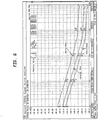
- FIG. 5 there is shown simulated phase noise plots of prior art oscillators (e.g., FIGS. 1 and 2 ) along with an oscillator implemented as shown in e.g. FIG.3 .
- the components of the circuit elements shown in FIGS. 1 , 2 and 3 were selected such that the circuitry oscillates at approximately 622 MHz (e.g., SONET OC-12 signal rate).
- the curve labeled S corresponds to operation of a series mode resonator as shown for example in FIG. 2 .
- the curve labeled P depicts the performance of a parallel mode resonator as shown for example in FIG. 1 .
- the curve labeled H depicts the performance of a hybrid tuned resonator oscillator as shown for example in FIG. 3 .
- the performance of the hybrid-mode resonator oscillator result in improvement of the phase noise performance of the oscillator 30 as compared to the oscillators 100, 118.
- FIG. 6 there is shown a comparison of the measured phase noise plot of the prior art resonators as shown for example in FIGS. 1 and 2 , along with a hybrid mode resonator oscillator implemented as shown in e.g., FIG. 3 .
- the measured phase noise was anywhere from 6 to 10 db better for a hybrid mode resonator oscillator as compared to those of the prior art.
- the phase noise plots of FIG. 6 were measured on circuits in which components were chosen so that the frequency of oscillation was approximately 622 MHz.
- the circuit elements of the foregoing oscillators may be chosen that the frequency of the circuit can oscillate at frequencies other then 622 MHz.
- the tuning network may be used to tune the frequency of oscillation over a tuning band.
- the oscillator 700 preferably includes a transistor 710 having a collector terminal C, a base terminal B and an emitter terminal E.
- the oscillator 700 also includes first and second feedback capacitors C1 and C1 connected in series between the base B of the transistor 710 and ground.
- a series tuned resonator 714 and a parallel tuned resonator 718 are coupled to the base terminal B as shown.
- a temperature compensating resistor Rtc is coupled between emitter terminal E and the feedback capacitors C1, C2.
- the resistor Rtc is generally used to compensate for thermal drift during operation of the oscillator.
- Two stage filtering is provided at the emitter terminal E via a first filter 720 and a second filter 722.
- the first filter 720 preferably comprises an LC filter and the second filter 722 preferably comprises a RC filter as shown. Together the first and second filters 720 and 722 are operable to provide two stage regenerative filtering, which reduces the noise spectral density of the transistor 710.
- a noise feedback and DC bias network 730 is coupled between the collector terminal C and the base terminal B of the transistor 710.
- the noise feedback and DC bias network 730 is operable to keep the bias voltage appearing at the collector C constant. As such, temperature variations that may occur and cause the bias voltage to change during operation of the oscillator 700 tend not to influence the operation of the transistor 710 and, therefore, the oscillator 700.
- the noise feedback and DC bias network 730 includes one or more transistors, such transistors 732, 733. These transistors 732, 733 and the arrangement of the other circuit elements comprising the network 730 feedback a select amount of phase noise present at the collector terminal C into the base terminal B. As the bias condition of the transistor 710 changes due to a change in the operating temperature, the network 730 adjusts the phase noise fed back to the terminal B and in this way compensates for changes in temperature.
- the oscillator 700 further includes a tuning network 740.
- the tuning network 740 includes a tuning voltage source Vtune. Changing the voltage of Vtune changes the oscillating frequency of the circuit 700 and the signal appearing at Pout.
- the tuning network 740 also includes a pair capacitor Cv coupled in parallel with first and second diodes 742, 743 across inductor L3.
- a third diode 744 and fourth diode 745 are coupled in parallel between the inductor L3 and inductor L2 as shown.
- a noise filtering network 750 is coupled across the tuning network 740 and the filter 722.
- the oscillator 700 operates in accordance with the hybrid mode principles described above but includes the additional features of temperature compensation via the network 730 and resistor Rtc.
- the oscillator 700 further includes two stage regenerative filtering and a noise filtering networks as discussed above. These additional features serve to improve the noise performance of the oscillator 700 versus those shown in FIGS. 3 and 4 .
- FIG. 7 operates in a dynamically controlled dual resonance mode by incorporating a hybrid resonance and noise filtering network in such a way that the noise impedance transfer function for a wide tuning range is optimized. As such, it provides user definable low noise signal sources for different frequency bands in comparison to a fixed phase hits sensitive ceramic/SAW resonator based VCOs, which are known to be generally expensive.
- the series resonance block 714 provides better tuning range at the cost of loading thereby degrading the phase noise performance.
- the block 718 operates in a parallel resonance mode thereby providing low phase noise performance at the cost of a limited tuning range. Although by combing blocks 714 and 718 better tuning range may be achieved along with low phase noise performance, it is achieved only for fixed frequencies.
- FIGS. 6 , 9 and 10 show the phase noise performance for the different modes (series, parallel and hybrid).
- ⁇ f f1 - f2; where f1 is the resonant frequency of block 718 and f2 is the resonant frequency of block 718) dynamically the frequency of operation can be extended without significantly compromising on output power and phase noise performance. Therefore, FIG. 7 shows a user-definable phase hit insensitive oscillator circuit that provides improved phase noise performance in comparison to the individual series resonance mode or parallel resonance, which is usually done using expensive CROs or SAWs.
- An additional advantage of hybrid resonance mode is that thermal drift (change in oscillating frequency due change in operating temperature and other parameters) may be significantly minimized by optimizing delta f either positively or negatively, depending on temperature gradient. For example, depending on the temperature gradient delta f may be positive, negative or zero.
- An aspect of the present invention is also that by using two low Q resonators in a planar domain such 714, 718 (or as shown in FIG. 11 , 1130, 1140) provides high Q resonance, the required tuning range result in low cost, power efficient oscillator that can replace discrete expensive, bulky CRO or SAW resonator while providing better phase noise performace. Such performance is depicted is in FIG. 12 for example.
- the oscillator 800 includes for the most part the same functional blocks as shown in FIG. 7 . In that regard, those blocks have been labeled as shown in FIG. 7 where appropriate.
- the parallel tuned oscillator 830 comprises a printed coupled resonator in a distributed domain such as mirco-stripline, stripline or suspended stripline.
- Stripline technology generally refers to a specific transmission line on a PCB where the signal trace is buried within the PCB and is spaced above and below a ground plane by the dielectric material, such as FR-4 or Roger material.
- Micro-stripline generally refers to a planar waveguide fabricated in a similar manner to an integrated circuit, or even printed onto a substrate. Suspended-stripline is similar in structure to ordinary stripline, but instead of disposing a ground plane on the dielectric substrate, as in stripline, the dielectric substrate is suspended in space, usually in air, between two ground planes. By replacing the lumped resonator with a resonator in distributed domain, the time average loaded Q is improved and the oscillator becomes less prone to phase hits.
- FIG. 9 depicts the simulated phase noise performance of the two prior art oscillator of FIGS. 1 and 2 as compared to an oscillator of FIG. 7 .
- the curve labeled S is for a series mode resonator
- P is for a parallel mode resonator
- H is for a hybrid mode resonator as shown in FIG. 7 .
- FIG. 10 shows the measured phase for such circuits. The results shown in FIGS. 9 and 10 were for oscillators where the circuit components were chosen so that the circuit operates at approximately 1000 MHz.
- FIG. 11 is a circuit diagram illustrating an oscillator in accordance with an additional aspect of the present invention.
- the oscillator of FIG. 11 includes two transistors 1110, 1120 arranged in a cascade configuration along with a noise feedback bias circuitry, a dynamic tracking filter at the output (which is taken from the collector), a dynamically tuned conduction angle, noise filtering and integrated coupled resonators 1130, 1140.
- the resonators 1130, 1140 may be implemented in stripline, micro-stripline or suspended stripline as discussed above.
- FIGS. 12 and 13 depict the performance of a 2.488 GHz oscillator implemented in accordance with the present invention as compared to the performance of prior art oscillators operating at the same frequency.
- the present invention provides reduction and/or elimination of phase hits that may occur in an oscillator without sacrificing the phase noise performance and the tuning range of the oscillator.
- the oscillator is based on a topology that supports fast convergence by using a dynamically tuned distributed coupled resonator/inductor for optimum noise performance over the frequency band.
- the circuit topology and layout of the resonator is selected in such a way that it supports uniform negative resistance over the tuning range.
- the high Q resonator SAW or Ceramic resonator
- the high Q resonator is preferably replaced by a printed coupled resonator in a distributed domain (microstrip line, stripline, suspended stripline). This results in relative improvement in the time average loaded Q when compared to an uncoupled lumped or distributed resonator.
- such a resonator is typically less prone to phase hits (printed planar coupled resonators are free from ceramic material, which is prone to phase hits) over the tuning range.
- DCRs distributed coupled resonators
- CROs/SAWs which are depicted much like a high Q planar resonator in an equivalent circuit, can achieve the phase-noise performances of a CRO oscillator but over a wider tuning and operating temperature range at a lower cost. They may be made small compared to CROs/SAWs, especially at frequencies of 1000 MHz and less, and can be readily designed at standard and custom frequencies up to about 10 GHz without expensive NRE costs.
- the DCR topology acts as a Q-multiplier, which employs a hybrid resonance mode, a regenerative noise filtering network, and noise feedback bias circuit.
- the noise feedback circuit is incorporated in the topology to reduce thermal drift over a wide temperature range.
- the mode coupling approach includes a methodology for the DCR to enhance the dynamic loaded Q, and to reduce or eliminate phase hits, while reducing the susceptibility to microphonics to an extremely low level, and retaining low phase noise and broadband tunability.
- the present invention provides an apparatus and method for increasing the Q value of a printed planar resonator by cascading a plurality of units, which include a passive frequency selective circuit such as distributed coupled resonators having multiple coupled lines to obtain an oscillator exhibiting a relatively high Q resonator in comparison to uncoupled printed resonators.
- a passive frequency selective circuit such as distributed coupled resonators having multiple coupled lines to obtain an oscillator exhibiting a relatively high Q resonator in comparison to uncoupled printed resonators.
- a plurality of distributed resonators are cascaded or concatended to increase the phase derivative, or group delay [ ⁇ / ⁇ ] of the resonator.
- the phase condition of the oscillator circuit occurs in the steepest part of the phase characteristics of the resonator.
- modifying the transfer function of the parallel mode resonance by introducing a series tuned resonance shifts the oscillating frequency of the oscillator circuit but improves the group delay based on the selection of the component values of the series tuned resonator network. Therefore, the shifted oscillating frequency due to the addition of the series mode resonance may substantially coincide with a maximum-slope of the phase characteristic curve of the oscillator circuit.
- the operation of the oscillator circuit about this point results in the circuit operating within the lowest phase noise domain of the phase characteristic curve, thereby improving the effective dynamic loaded Q.
- This increase in effective dynamic loaded Q translates directly into reduced phase noise.
- an oscillator implemented in accordance with this aspect of the present invention may be readily and advantageously employed without otherwise sacrificing component size or other economic consideration.
- an aspect of the present invention in furtherance of satisfying a long-felt and growing need in the field, facilitates an oscillator having relatively low phase hits for a given physical size along with other attributes known to be desirable in the art.
- phase hits are generally attributable to microphonic noise and its associated circuitry. Circuitry that reduces the microphonic noise will typically reduce the phase hits associated with such circuitry. Lower microphonics noise generally means that the resonator network should be free from ceramic material.
- the present invention discloses a topology for providing a low phase noise and minimum phase hits when compared to the ceramic and SAW resonator based oscillators. The topology is based on a hybrid resonance network, which improves the loaded Q of the lumped or printed resonator tuned in parallel resonance mode by incorporating a series resonance mode network.
- the topology of the invention preferably eliminates the use of ceramic material in the oscillator circuit, thereby allowing the oscillator circuit to be operated in a relatively low Q environment at a higher oscillation frequency. This provides a wider tuning range than a CRO based oscillator circuit without compromising the phase noise performance.
- Improvements in phase noise performance may be obtained in accordance with the foregoing aspects of the present invention by incorporating an additional series resonance tuning network into the parallel tuned oscillator circuit. This allows the steepest phase region to coincide with a maximum-slope inflection point of the phase characteristic curve. This leads to improvement of loaded Q that translates directly into reduced phase noise.
- the improvement obtainable using the technique of the present invention is typically in the range of 6-10 dB.
- An oscillator includes a resonant structure selected to resonate at a frequency, and an active device coupled in parallel to the resonant structure.
- the active impedance created by the active device includes a negative real part with a real magnitude and an imaginary part with an imaginary magnitude.
- the real magnitude is a function of the imaginary magnitude and the imaginary magnitude is selected such that the real magnitude compensates for the losses in the resonator while coinciding with a maximum-slope inflection point of the phase characteristic curve for improved group delay.
- the resonator structure is, preferably, a resonator such as a lumped resonator, which preferably comprises a parallel inductance and capacitance or printed resonator in a distributed medium (microstrip line, stripline, suspended stripline etc.).
- the resonant structure may be selected to have a parallel resonant frequency that is below the desired or nominal operating frequency of the oscillator.
- a series tuned resonator network in conjunction with a parallel tuned resonator network the impedance level at the oscillator frequency is improved. This supports a relatively large voltage swing and improvement in the signal -to noise ratio of the oscillator circuit.
- a wideband oscillator circuit may be obtained with the phase requirements for simultaneously tuning the series and parallel resonance conditions over the tuning band. This is desirably achieved by frequency locking a first parallel tuned resonator with at least a second series tuned resonator to provide the steepest phase characteristics and a wider tuning range.
- Another aspect of the present invention is provision of an effective and manufacturable circuit.
- a (distributed coupled resonator) DCR is relatively easy to manufacture as compared to a CRO and a SAW because its planar nature, it is therefore amenable for integration in chip form.
- the present invention also advantageously allows for generation of low phase noise oscillation signals for a PLL application.
- the present invention offers a power efficient and cost-effective alternative to the ceramic and SAW-resonator based oscillator. More specifically, in accordance with this aspect of the present invention, the hybrid-tuned approach (combination of parallel and series resonance mode) is employed by using a cascode configuration of an active device, regenerative filtering, which basically improves the signal to noise ratio and filters the noise at the fundamental frequency, thereby improving the time average loaded Q of the resonator.
- the present invention allows improving the loaded Q of an oscillator by independently resonating a first parallel tuned circuit with a second series tuned circuit and combining the outputs of the first and second circuits.
- the oscillator circuit comprises at least two independent tuning networks.
- the series and parallel-coupled resonator networks or circuits desirably improve the time average Q over the frequency band.
- Tuning the oscillator/VCO may be included to account for temperature differences or component variations.
- a means for supplying energy as a buffer to a parallel tuned resonator in an oscillator circuit may be provided by using an additional series mode tuned network.
- Use of a series resonance network or low impedance tuned network results in a transiently sharp change of the phase with respect to the operating frequency of the oscillator, thereby improving phase noise performance.
- ultra low noise oscillators can be made with a degree of accuracy previously attainable only by much more complex and costly resonators such as SAW and ceramic resonators.
- the present invention allows for dynamic tracking of the resonance mode, negative resistance, noise filter and tracking output filter of an oscillator, thereby dynamically tuning the oscillator frequency band, which results in relatively low phase noise and low microphonics. Furthermore, power efficiency is increased by reduction of the DC current by incorporating two 3-terminal devices in cascode configuration (transistors Q 1 and Q 2 are in the common collector and emitter configuration) so that both the device share the same emitter current.
- the basic structure may be extended for other applications that have similar kind of requirements.
- a voltage-controlled oscillator implemented in accordance with the present invention may be employed in any number of devices that are used to communicate on data, telephone, cellular or, in general, communications network. Such devices may include but are not limited to, for example, cellular phones, personal digital assistants, modem cards, lap tops, satellite telephones.
- the oscillator circuitry shown in the various drawings and described above may be employed in a PLL to either generate a clock signal that may be used to transmit or recover information transmitted or received over a network.
- the circuitry of the present invention may be employed in wired networks, satellite networks, etc.
- the active device comprises three terminal device that can provide a 180 degree phase shift between any two ports.
Landscapes
- Inductance-Capacitance Distribution Constants And Capacitance-Resistance Oscillators (AREA)
Claims (15)
- Spannungsgesteuerter Oszillator (300; 400; 700) zum Kombinieren von Serien- und Parallelresonanzmodi, mit:einer aktiven Vorrichtung (304; 710; 1120; 1110) mit einem ersten, einem zweiten und einem dritten Anschluss zum Vergrößern eines Signals zwischen dem zweiten Anschluss und dem ersten Anschluss und zum Bereitstellen einer Phasenverschiebung um 180 Grad zu dem Signal;einer Vorspannungsschaltung, die mit dem ersten Anschluss gekoppelt ist;einem ersten Resonatorschaltkreis für einen Serienresonanzmodus (316; 714; 1130) mit einem ersten und einem zweiten Resonatoranschluss, dessen zweiter Resonatoranschluss mit dem zweiten Anschluss gekoppelt ist, wobei der erste Resonatorschaltkreis (316; 714; 1130) eine erste Resonanzfrequenz aufweist; einem zweiten Resonatorschaltkreis (310; 410; 718; 830; 1140) für einen parallelen Resonanzmodus gekoppelt mit einem Knoten zwischen dem zweiten Anschluss und dem ersten Resonatorschaltkreis, wobei der zweite Resonatorschaltkreis eine zweite Resonanzfrequenz aufweist, die sich von der ersten Resonanzfrequenz unterscheidet;einem Abstimmnetzwerk (320; 740) gekoppelt mit dem ersten Resonatoranschluss des zweiten Resonatorschaltkreises (316; 714; 1130);einem ersten Filter (720), der mit dem dritten Anschluss der aktiven Vorrichtung (304; 710; 1120, 1110) gekoppelt ist, und einem zweiten Filter (722), der in Serie mit dem ersten Filter (720) gekoppelt ist;
gekennzeichnet durchein Geräuschfilternetzwerk (750), das zwischen dem Abstimmnetzwerk (320; 740) und dem Verbindungsknoten zwischen dem ersten und dem zweiten Filter (720; 722) gekoppelt ist und einen mit dem Abstimmnetzwerk (320; 740) gekoppelten ersten Induktor (Ln2), einen in Serie mit dem ersten Induktor (Ln2) gekoppelten zweiten Induktor (Ln1), einen ersten Kondensator (Cen1), der zwischen einem Verbindungsknoten zwischen dem ersten und dem zweiten Induktor (Ln2, Ln1) und Masse gekoppelt ist, einen zweiten Kondensator (Cen2), der in Serie mit dem zweiten Induktor (Ln1) und mit dem Verbindungsknoten zwischen dem ersten und dem zweiten Filter (720; 722) gekoppelt ist, und mindestens eine Diode aufweist, die zwischen dem Verbindungsknoten zwischen dem zweiten Induktor (Ln1) und dem zweiten Kondensator (Cen2) und Masse gekoppelt ist. - Spannungsgesteuerter Oszillator nach Anspruch 1,
wobei der erste und der zweite Resonatorschaltkreis (310, 316; 410; 718, 714; 830; 1140; 1130) jeweils ein konzentriertes Induktor-Kondensator-Paar aufweisen. - Spannungsgesteuerter Oszillator nach Anspruch 2,
wobei das konzentrierte Induktor-Kondensator-Paar des ersten Resonatorschaltkreises einen ersten Induktor in Serie mit einem ersten Kondensator aufweist. - Spannungsgesteuerter Oszillator nach Anspruch 3,
wobei das konzentrierte Induktor-Kondensator-Paar des zweiten Resonatorschaltkreises (316; 714; 1130) einen zweiten Induktor (Lp) parallel zu einem zweiten Kondensator (Cp) aufweist. - Spannungsgesteuerter Oszillator nach Anspruch 1,
wobei der erste Resonatorschaltkreis (316; 714; 1130) einen verteilten Resonator aufweist, der in einer verteilten Domäne ausgebildet ist, welche aus der Gruppe bestehend aus einer Mikrobandleitungs-, Bandleitungs- oder aufgehängten Bandleitungsspur ausgewählt ist. - Spannungsgesteuerter Oszillator nach Anspruch 1, wobei die aktive Vorrichtung (304; 710; 1120, 1110) einen bipolaren Transistor (Q1) mit seinem Kollektoranschluss (C) als erstem Anschluss, seinem Basisanschluss (B) als zweitem Anschluss und seinem Emitteranschluss (E) als drittem Anschluss aufweist.
- Spannungsgesteuerter Oszillator nach Anspruch 6, weiterhin mit:einem ersten Rückkopplungskondensator (C1), der zwischen dem Emitter und Basisanschlüssen gekoppelt ist;einem zweiten Rückkopplungskondensator (C2), der mit dem Emitteranschluss gekoppelt ist; undwobei der erste Filter (720) einen LC Filter (Le1, Cv) aufweist und der zweite Filter (722) einen RC Filter (RE, Ca2) aufweist, so dass beide Filter betätigbar sind, um zweistufiges regeneratives Filtern bereitzustellen, und der Induktor des ersten Filters, ein RF Drosselinduktor (Le2) und der Widerstand des zweiten Filters in dieser Reihenfolge in Serie miteinander mit dem Emitteranschluss gekoppelt sind.
- Spannungsgesteuerter Oszillator nach Anspruch 7, weiterhin mit einem Rückkopplungsschaltkreis (730), der zwischen dem Kollektor und Basisanschlüssen gekoppelt ist, wobei der Rückkopplungsschaltkreis betätigbar ist, um eine ausgewählte Menge an Phasenrauschen, das an dem Kollektoranschluss auftritt, in den Basisanschluss zurück zu koppeln.
- Spannungsgesteuerter Oszillator nach Anspruch 8, wobei der Rückkopplungsschaltkreis (730) einen ersten Rückkopplungstransistor und einen zweiten Rückkopplungstransistor aufweist.
- Spannungsgesteuerter Oszillator nach Anspruch 9, weiterhin mit einem Widerstand (Rtc), der zwischen einem Verbindungsknoten zwischen dem Emitter und dem ersten Filter und einem Verbindungsknoten zwischen dem ersten und dem zweiten Rückkopplungskondensator gekoppelt ist.
- Spannungsgesteuerter Oszillator nach Anspruch 1 oder 5, wobei der zweite Resonatorschaltkreis (310; 410; 718; 830; 1140) ein Resonatornetzwerk aufweist, das aus der Gruppe bestehend aus einer Bandleitung, einer Mikrobandleitung oder einer aufgehängten Bandleitung ausgewählt ist.
- Netzwerkkommunikationseinrichtung, wobei die Vorrichtung Folgendes aufweist:eine Phasenregelschleife zum Erzeugen eines Taktsignals, das zum Übertragen oder Wiederherstellen von Informationen eingesetzt wird, die von der oder an die Vorrichtung übermittelt werden,wobei die Phasenregelschleife einen spannungsgesteuerten Oszillator nach Anspruch 7 zum Erzeugen des Taktsignals aufweist.
- Kommunikationseinrichtung nach Anspruch 12, wobei die Kommunikationseinrichtung ein drahtloses Gerät enthält.
- Kommunikationseinrichtung nach Anspruch 13, wobei das drahtlose Gerät ein Mobiltelefon ist.
- Kommunikationseinrichtung nach Anspruch 13, wobei das drahtlose Gerät ein Personal Digital Assistant ist.
Applications Claiming Priority (2)
| Application Number | Priority Date | Filing Date | Title |
|---|---|---|---|
| US68353305P | 2005-05-20 | 2005-05-20 | |
| PCT/US2006/019398 WO2006127442A1 (en) | 2005-05-20 | 2006-05-19 | Tunable oscillator having series and parallel tuned resonant circuits |
Publications (2)
| Publication Number | Publication Date |
|---|---|
| EP1886403A1 EP1886403A1 (de) | 2008-02-13 |
| EP1886403B1 true EP1886403B1 (de) | 2018-12-26 |
Family
ID=36940481
Family Applications (1)
| Application Number | Title | Priority Date | Filing Date |
|---|---|---|---|
| EP06760164.1A Not-in-force EP1886403B1 (de) | 2005-05-20 | 2006-05-19 | Einstellbarer oszillator mit serien- und parallelresonanzkreisen |
Country Status (5)
| Country | Link |
|---|---|
| US (1) | US7636021B2 (de) |
| EP (1) | EP1886403B1 (de) |
| CA (1) | CA2608203C (de) |
| RU (1) | RU2404505C2 (de) |
| WO (1) | WO2006127442A1 (de) |
Families Citing this family (19)
| Publication number | Priority date | Publication date | Assignee | Title |
|---|---|---|---|---|
| DE102006017189B4 (de) * | 2006-04-12 | 2010-10-21 | Atmel Automotive Gmbh | Integrierte Oszillatorschaltung mit wenigstens zwei Schwingkreisen |
| US20080102761A1 (en) * | 2006-10-27 | 2008-05-01 | Stratex Networks, Inc. | System and method for compensation of phase hits |
| EP2087623B1 (de) * | 2006-11-03 | 2010-07-14 | RF Magic, Inc. | Frequenzübertragung und stapelung von satellitensignalen |
| EP2456143A1 (de) | 2007-02-14 | 2012-05-23 | Entropic Communications Inc. | Parametrisierte Dienstgüte in einem Netzwerk |
| US7884677B2 (en) * | 2007-04-19 | 2011-02-08 | Marvell World Trade Ltd. | Method and apparatus for reducing phase noise in an oscillator signal of a Colpitts oscillator |
| JP4782217B2 (ja) * | 2009-06-08 | 2011-09-28 | 日本電波工業株式会社 | 低雑音電圧制御発振回路 |
| TWI483542B (zh) * | 2009-07-10 | 2015-05-01 | Chi Mei Comm Systems Inc | 放大器電路 |
| RU2483427C9 (ru) * | 2011-04-01 | 2013-12-10 | Евгений Васильевич Прокофьев | Способ генерирования регламентируемых колебаний |
| US8773211B2 (en) | 2011-11-25 | 2014-07-08 | Intel Mobile Communications GmbH | Common mode rejection circuit |
| WO2014108745A1 (en) * | 2013-01-09 | 2014-07-17 | Freescale Semiconductor, Inc. | Voltage controlled oscillator |
| CN103475339A (zh) * | 2013-09-10 | 2013-12-25 | 昆山新金福精密电子有限公司 | 一种多谐振荡电路 |
| US9853646B2 (en) | 2015-01-08 | 2017-12-26 | Maxlinear Asia Singapore PTE LTD | System, method and apparatus for phase hits and microphonics cancellation |
| US9753068B2 (en) * | 2015-01-14 | 2017-09-05 | Insitu Inc. | Systems and methods for signal quantization |
| US10153727B2 (en) | 2016-05-12 | 2018-12-11 | International Business Machines Corporation | Transformer based shielded oscillator |
| CN109613523B (zh) * | 2018-10-23 | 2023-04-07 | 南通赛洋电子有限公司 | 一种测探仪信号预处理电路 |
| CN112564625A (zh) * | 2019-09-25 | 2021-03-26 | 天津大学 | 一种基于sisl的多谐振压控振荡器 |
| US10951182B1 (en) * | 2020-01-02 | 2021-03-16 | Keycore Technology Corp. | Millimeter wave power amplifier circuit and millimeter wave power amplifier device |
| US11323302B2 (en) | 2020-03-06 | 2022-05-03 | Huawei Technologies Co., Ltd. | Detection and mitigation of oscillator phase hit |
| US11323070B1 (en) * | 2021-04-16 | 2022-05-03 | Apple Inc. | Oscillator with fin field-effect transistor (FinFET) resonator |
Citations (1)
| Publication number | Priority date | Publication date | Assignee | Title |
|---|---|---|---|---|
| US4378532A (en) * | 1979-04-02 | 1983-03-29 | Hewlett Packard Company | Oscillator mode suppression apparatus having bandpass effect |
Family Cites Families (83)
| Publication number | Priority date | Publication date | Assignee | Title |
|---|---|---|---|---|
| US2524035A (en) * | 1948-02-26 | 1950-10-03 | Bell Telphone Lab Inc | Three-electrode circuit element utilizing semiconductive materials |
| US2502488A (en) * | 1948-09-24 | 1950-04-04 | Bell Telephone Labor Inc | Semiconductor amplifier |
| US3373379A (en) * | 1966-06-17 | 1968-03-12 | Motorola Inc | Crystal oscillator with temperature compensation |
| US3624550A (en) * | 1969-06-16 | 1971-11-30 | Varian Associates | Microwave oscillator circuit for a bulk-effect negative-resistance device |
| US4338576A (en) * | 1978-07-26 | 1982-07-06 | Tdk Electronics Co., Ltd. | Ultrasonic atomizer unit utilizing shielded and grounded elements |
| US4310809A (en) * | 1979-04-27 | 1982-01-12 | Westinghouse Electric Corp. | Low noise microstrip voltage controlled oscillator |
| JPS5726902A (en) * | 1980-07-25 | 1982-02-13 | Hitachi Ltd | Fet oscillation circuit |
| DE3166196D1 (en) * | 1980-11-03 | 1984-10-25 | Siemens Ag | Oscillation circuit which may take the form of an integrated circuit |
| DE3136348A1 (de) * | 1981-09-14 | 1983-03-24 | Philips Patentverwaltung Gmbh, 2000 Hamburg | Mikrowellen-oszillator in gegentaktschaltung |
| JPS5972205A (ja) | 1982-10-18 | 1984-04-24 | Ricoh Co Ltd | アナログ量検知用lc発振器の周波数可変方法 |
| JPS59139708A (ja) | 1983-01-27 | 1984-08-10 | Fujitsu Ltd | 圧電振動発振器 |
| US4619001A (en) * | 1983-08-02 | 1986-10-21 | Matsushita Electric Industrial Co., Ltd. | Tuning systems on dielectric substrates |
| JPS60190004A (ja) * | 1984-03-09 | 1985-09-27 | Matsushita Electric Ind Co Ltd | 発振回路 |
| DE3443446A1 (de) | 1984-11-29 | 1986-05-28 | ANT Nachrichtentechnik GmbH, 7150 Backnang | Abstimmvorrichtung fuer einen spannungsgesteuerten oszillator |
| US4633197A (en) * | 1985-03-29 | 1986-12-30 | Motorola, Inc. | Single resonant tank modulated oscillator |
| US4661785A (en) * | 1985-05-22 | 1987-04-28 | S. T. Research Corporation | Balanced feedback oscillators |
| US4621241A (en) * | 1985-06-07 | 1986-11-04 | Vari-L Company, Inc. | Wide range electronic oscillator |
| US4677396A (en) * | 1985-12-06 | 1987-06-30 | Zenith Electronics Corporation | Surface mounted component UHF oscillator |
| US4692714A (en) * | 1986-10-20 | 1987-09-08 | Raytheon Company | Single resonator push-push oscillator |
| US4812784A (en) * | 1987-11-19 | 1989-03-14 | International Business Machines Corporation | Temperature stable voltage controlled oscillator with super linear wide frequency range |
| FR2625051B1 (fr) * | 1987-12-18 | 1990-04-20 | Thomson Hybrides Microondes | Oscillateur doubleur de frequence, accorde par varactors |
| US5053649A (en) * | 1988-12-21 | 1991-10-01 | Ultra Network Technologies | Method and apparatus for high speed phase detection |
| JPH0354903A (ja) * | 1989-03-31 | 1991-03-08 | Kyocera Corp | 発振回路 |
| US5231361A (en) * | 1990-02-05 | 1993-07-27 | Trw Inc. | Voltage controlled push-push oscillator with parallel resonant tank circuits |
| US5142255A (en) * | 1990-05-07 | 1992-08-25 | The Texas A&M University System | Planar active endfire radiating elements and coplanar waveguide filters with wide electronic tuning bandwidth |
| JP2847573B2 (ja) | 1990-09-10 | 1999-01-20 | 富士通株式会社 | 電圧制御発振器 |
| US5041799A (en) * | 1990-11-05 | 1991-08-20 | Motorola, Inc. | Temperature compensation circuit for a crystal oscillator |
| US5223801A (en) * | 1992-03-30 | 1993-06-29 | Interactive Technologies, Inc. | Crystal oscillator and transmitter operating at the third harmonic of the fifth overtone of a crystal |
| ATE196703T1 (de) * | 1992-04-03 | 2000-10-15 | Siemens Ag Oesterreich | Oszillator für eine frequenz von 1,6 bis 3 ghz |
| US5373264A (en) * | 1993-01-21 | 1994-12-13 | Hewlett-Packard Company | Negative resistance oscillator with electronically tunable base inductance |
| US5363067A (en) * | 1993-05-19 | 1994-11-08 | Motorola, Inc. | Microstrip assembly |
| US5402087A (en) * | 1994-04-08 | 1995-03-28 | B.E.L.-Tronics Limited | Voltage controlled push-push oscillator |
| US5650754A (en) * | 1995-02-15 | 1997-07-22 | Synergy Microwave Corporation | Phase-loched loop circuits and voltage controlled oscillator circuits |
| RU2128873C1 (ru) * | 1995-12-21 | 1999-04-10 | Войсковая часть 11135 | Управляемый кварцевый генератор с умножением частоты |
| JPH09270602A (ja) | 1996-04-01 | 1997-10-14 | Matsushita Electric Ind Co Ltd | 受信装置 |
| US5748051A (en) * | 1996-05-16 | 1998-05-05 | Z-Communications, Inc. | Low phase noise UHF and microwave oscillator |
| US5661439A (en) * | 1996-07-11 | 1997-08-26 | Northrop Grumman Corporation | Method and apparatus for cancelling phase noise |
| JPH1051234A (ja) | 1996-08-05 | 1998-02-20 | Tdk Corp | 電圧制御発振器およびその調整方法 |
| US5821410A (en) * | 1996-09-20 | 1998-10-13 | Regents Of The University Of California | Scanning tip microwave near field microscope |
| JPH10209714A (ja) | 1996-11-19 | 1998-08-07 | Sharp Corp | 電圧制御通過帯域可変フィルタおよびそれを用いる高周波回路モジュール |
| DE19652146B4 (de) * | 1996-12-14 | 2006-06-29 | Sennheiser Electronic Gmbh & Co. Kg | Rauscharme Oszillatorschaltung |
| US5856763A (en) * | 1997-03-05 | 1999-01-05 | Motorola Inc. | Dual frequency voltage controlled oscillator |
| US6172577B1 (en) * | 1997-07-25 | 2001-01-09 | Murata Manufacturing Co., Ltd. | Oscillator and oscillation apparatus using the oscillator |
| US5854578A (en) * | 1997-09-15 | 1998-12-29 | Motorola, Inc. | Active circuit having a temperature stable bias |
| US6091309A (en) * | 1998-01-26 | 2000-07-18 | Burke; Joseph P. | Tunable low noise oscillator using delay lines and ring mode trap filter |
| US6124767A (en) * | 1998-05-21 | 2000-09-26 | Delphi Components, Inc. | RF/Microwave oscillator |
| FI106894B (fi) * | 1998-06-02 | 2001-04-30 | Nokia Mobile Phones Ltd | Resonaattorirakenteita |
| KR100290285B1 (ko) * | 1999-01-13 | 2001-05-15 | 윤종용 | 프리스케일러의 입력 버퍼 |
| JP3283493B2 (ja) * | 1999-02-02 | 2002-05-20 | 東洋通信機株式会社 | 高安定度圧電発振器 |
| US6321074B1 (en) * | 1999-02-18 | 2001-11-20 | Itron, Inc. | Apparatus and method for reducing oscillator frequency pulling during AM modulation |
| US6326854B1 (en) * | 1999-09-30 | 2001-12-04 | Nortel Networks Limited | Coaxial resonator and oscillation circuits featuring coaxial resonators |
| US6429748B2 (en) * | 1999-09-30 | 2002-08-06 | Nortel Networks Limited | Oscillation circuits featuring coaxial resonators |
| US6297704B1 (en) | 1999-09-30 | 2001-10-02 | Nortel Networks Corporation | Oscillation circuits featuring coaxial resonators |
| NL1013936C2 (nl) * | 1999-12-23 | 2001-06-26 | Ericsson Telefon Ab L M | Oscillator, zender voorzien van een dergelijke oscillator, en gebruik van een dergelijke zender. |
| JP2001185951A (ja) * | 1999-12-24 | 2001-07-06 | Murata Mfg Co Ltd | 電圧制御発振器および通信装置 |
| JP3818624B2 (ja) * | 2000-02-23 | 2006-09-06 | 株式会社ルネサステクノロジ | 無線通信システム |
| JP2001308638A (ja) * | 2000-04-18 | 2001-11-02 | Alps Electric Co Ltd | 電圧制御発振器 |
| JP2001313526A (ja) * | 2000-04-27 | 2001-11-09 | Murata Mfg Co Ltd | 発振器および通信装置 |
| DE10033741B4 (de) | 2000-07-12 | 2012-01-26 | Synergy Microwave Corp. | Oszillatorschaltung |
| US6462627B1 (en) | 2000-08-25 | 2002-10-08 | Tropian Inc. | Oscillator circuit having reduced phase noise |
| DE60142055D1 (de) * | 2000-08-31 | 2010-06-17 | Citizen Holdings Co Ltd | Temperaturkompensationsoszillator |
| JP2002261542A (ja) * | 2000-12-27 | 2002-09-13 | Murata Mfg Co Ltd | 発振器及びそれを用いた通信機 |
| US6466099B2 (en) * | 2001-01-03 | 2002-10-15 | Motorola, Inc. | Voltage controlled oscillator (VCO) in colpitts configuration |
| US7088188B2 (en) * | 2001-02-13 | 2006-08-08 | Telefonaktiebolaget Lm Ericsson (Publ) | Differential oscillator |
| US6486744B1 (en) * | 2001-05-16 | 2002-11-26 | Digital Microwave Corporation | Low phase noise voltage-controlled oscillator and method of using the same |
| US6630869B2 (en) * | 2001-06-27 | 2003-10-07 | Harris Corporation | Very low phase noise temperature stable voltage controlled oscillator |
| JP3921362B2 (ja) * | 2001-07-30 | 2007-05-30 | 日本電波工業株式会社 | 温度補償水晶発振器 |
| US6624726B2 (en) * | 2001-08-31 | 2003-09-23 | Motorola, Inc. | High Q factor MEMS resonators |
| JP4772255B2 (ja) * | 2001-12-28 | 2011-09-14 | 日本電波工業株式会社 | スロットラインを用いた高周波発振器 |
| TW522637B (en) * | 2002-02-22 | 2003-03-01 | Accton Technology Corp | Low-phase noise oscillator with a microstrip resonator |
| US6489853B1 (en) * | 2002-03-19 | 2002-12-03 | Z-Communications, Inc. | Low phase noise oscillator |
| WO2004045090A2 (en) * | 2002-11-13 | 2004-05-27 | Vectron International | Oscillator module incorporating looped-stub resonator |
| US6765444B2 (en) * | 2002-11-18 | 2004-07-20 | Neoaxiom Corporation | Cross clocked lock detector circuit for phase locked loop |
| US6859118B2 (en) * | 2003-01-02 | 2005-02-22 | Harris Corporation | System and method for an ultra low noise micro-wave coaxial resonator oscillator using ⅝ths wavelength resonator |
| GB2401263B (en) * | 2003-04-29 | 2006-01-11 | Motorola Inc | Wireless communication terminal and voltage controlled oscillator therefor |
| US20040227578A1 (en) * | 2003-05-14 | 2004-11-18 | Miikka Hamalainen | Acoustic resonance-based frequency synthesizer using at least one bulk acoustic wave (BAW) or thin film bulk acoustic wave (FBAR) device |
| US6917265B2 (en) | 2003-05-22 | 2005-07-12 | Synergy Microwave Corporation | Microwave frequency surface mount components and methods of forming same |
| US7196591B2 (en) | 2003-08-06 | 2007-03-27 | Synergy Microwave Corporation | Tunable frequency, low phase noise and low thermal drift oscillator |
| US7088189B2 (en) * | 2003-09-09 | 2006-08-08 | Synergy Microwave Corporation | Integrated low noise microwave wideband push-push VCO |
| US7292113B2 (en) * | 2003-09-09 | 2007-11-06 | Synergy Microwave Corporation | Multi-octave band tunable coupled-resonator oscillator |
| JP4939228B2 (ja) * | 2003-12-09 | 2012-05-23 | シナジー マイクロウェーブ コーポレーション | 熱ドリフトがユーザ指定可能な電圧制御発振器 |
| US7262670B2 (en) * | 2003-12-09 | 2007-08-28 | Synergy Microwave Corporation | Low thermal drift, tunable frequency voltage controlled oscillator |
| EP1589655B1 (de) * | 2004-04-21 | 2019-08-21 | Synergy Microwave Corporation | Spannungsgesteuerter Breitbandozzillator mit gekoppelten Resonatoren vom Dämpfungstyp |
-
2006
- 2006-05-19 EP EP06760164.1A patent/EP1886403B1/de not_active Not-in-force
- 2006-05-19 WO PCT/US2006/019398 patent/WO2006127442A1/en not_active Ceased
- 2006-05-19 RU RU2007147399/09A patent/RU2404505C2/ru active IP Right Revival
- 2006-05-19 CA CA2608203A patent/CA2608203C/en active Active
- 2006-05-19 US US11/438,047 patent/US7636021B2/en active Active
Patent Citations (1)
| Publication number | Priority date | Publication date | Assignee | Title |
|---|---|---|---|---|
| US4378532A (en) * | 1979-04-02 | 1983-03-29 | Hewlett Packard Company | Oscillator mode suppression apparatus having bandpass effect |
Also Published As
| Publication number | Publication date |
|---|---|
| US7636021B2 (en) | 2009-12-22 |
| EP1886403A1 (de) | 2008-02-13 |
| RU2007147399A (ru) | 2009-06-27 |
| RU2404505C2 (ru) | 2010-11-20 |
| CA2608203C (en) | 2012-09-18 |
| CA2608203A1 (en) | 2006-11-30 |
| US20060279368A1 (en) | 2006-12-14 |
| WO2006127442A1 (en) | 2006-11-30 |
Similar Documents
| Publication | Publication Date | Title |
|---|---|---|
| EP1886403B1 (de) | Einstellbarer oszillator mit serien- und parallelresonanzkreisen | |
| US20050156675A1 (en) | Integrated low noise microwave wideband push-push VCO | |
| US7586381B2 (en) | User-definable, low cost, low phase hit and spectrally pure tunable oscillator | |
| EP1589655B1 (de) | Spannungsgesteuerter Breitbandozzillator mit gekoppelten Resonatoren vom Dämpfungstyp | |
| EP1542354B1 (de) | Spannungsgesteuerter-, Push-push-, Breitband-, Mikrowellenoszillator mit sehr niedrigem Rausch | |
| US7292113B2 (en) | Multi-octave band tunable coupled-resonator oscillator | |
| EP1628390B1 (de) | Spannungsgesteuerter Breitbandoszillator or mit niedrigem Phasenrausch und einen abstimmbaren Hybridnetzwerk | |
| US7262670B2 (en) | Low thermal drift, tunable frequency voltage controlled oscillator | |
| US7605670B2 (en) | User-definable low cost, low noise, and phase hit insensitive multi-octave-band tunable oscillator | |
| EP1926207B1 (de) | Geräuscharmer, hybrideinstellbarer, spannungskontrollierter Breitband-Oszillator | |
| Rohde et al. | Distributed coupled resonator (DCR) oscillators/VCOs limit phase noise and phase hits | |
| JP4903570B2 (ja) | 周波数可変発振器 | |
| Florian et al. | Push-push X band GaInP/GaAs VCO with a fully monolithic microstrip resonator | |
| EP1619789B1 (de) | Frequenzstimmbarer Oszillator mit niedriger Temperaturabweichung | |
| Rohde et al. | User-Defined and Configurable CSRO | |
| HK1091603A (en) | Low noise, hybrid tuned wideband voltage controlled oscillator | |
| HK1091960A (en) | Low thermal drift, tunable frequency voltage controlled oscillator | |
| HK1082602A (en) | Integrated ultra low noise microwave wideband push-push vco |
Legal Events
| Date | Code | Title | Description |
|---|---|---|---|
| PUAI | Public reference made under article 153(3) epc to a published international application that has entered the european phase |
Free format text: ORIGINAL CODE: 0009012 |
|
| 17P | Request for examination filed |
Effective date: 20070227 |
|
| AK | Designated contracting states |
Kind code of ref document: A1 Designated state(s): AT BE BG CH CY CZ DE DK EE ES FI FR GB GR HU IE IS IT LI LT LU LV MC NL PL PT RO SE SI SK TR |
|
| DAX | Request for extension of the european patent (deleted) | ||
| 17Q | First examination report despatched |
Effective date: 20140205 |
|
| STAA | Information on the status of an ep patent application or granted ep patent |
Free format text: STATUS: EXAMINATION IS IN PROGRESS |
|
| GRAP | Despatch of communication of intention to grant a patent |
Free format text: ORIGINAL CODE: EPIDOSNIGR1 |
|
| STAA | Information on the status of an ep patent application or granted ep patent |
Free format text: STATUS: GRANT OF PATENT IS INTENDED |
|
| INTG | Intention to grant announced |
Effective date: 20180801 |
|
| RIN1 | Information on inventor provided before grant (corrected) |
Inventor name: PODDAR, AJAY KUMAR Inventor name: ROHDE, ULRICH L. Inventor name: ZHANG, HUA Inventor name: REBEL, REIMUND Inventor name: SCHOEPF, KLAUS JUERGEN |
|
| GRAS | Grant fee paid |
Free format text: ORIGINAL CODE: EPIDOSNIGR3 |
|
| GRAA | (expected) grant |
Free format text: ORIGINAL CODE: 0009210 |
|
| STAA | Information on the status of an ep patent application or granted ep patent |
Free format text: STATUS: THE PATENT HAS BEEN GRANTED |
|
| AK | Designated contracting states |
Kind code of ref document: B1 Designated state(s): AT BE BG CH CY CZ DE DK EE ES FI FR GB GR HU IE IS IT LI LT LU LV MC NL PL PT RO SE SI SK TR |
|
| REG | Reference to a national code |
Ref country code: GB Ref legal event code: FG4D |
|
| REG | Reference to a national code |
Ref country code: CH Ref legal event code: EP |
|
| REG | Reference to a national code |
Ref country code: DE Ref legal event code: R096 Ref document number: 602006057144 Country of ref document: DE |
|
| REG | Reference to a national code |
Ref country code: AT Ref legal event code: REF Ref document number: 1082814 Country of ref document: AT Kind code of ref document: T Effective date: 20190115 |
|
| REG | Reference to a national code |
Ref country code: IE Ref legal event code: FG4D |
|
| PG25 | Lapsed in a contracting state [announced via postgrant information from national office to epo] |
Ref country code: LV Free format text: LAPSE BECAUSE OF FAILURE TO SUBMIT A TRANSLATION OF THE DESCRIPTION OR TO PAY THE FEE WITHIN THE PRESCRIBED TIME-LIMIT Effective date: 20181226 Ref country code: LT Free format text: LAPSE BECAUSE OF FAILURE TO SUBMIT A TRANSLATION OF THE DESCRIPTION OR TO PAY THE FEE WITHIN THE PRESCRIBED TIME-LIMIT Effective date: 20181226 Ref country code: BG Free format text: LAPSE BECAUSE OF FAILURE TO SUBMIT A TRANSLATION OF THE DESCRIPTION OR TO PAY THE FEE WITHIN THE PRESCRIBED TIME-LIMIT Effective date: 20190326 Ref country code: FI Free format text: LAPSE BECAUSE OF FAILURE TO SUBMIT A TRANSLATION OF THE DESCRIPTION OR TO PAY THE FEE WITHIN THE PRESCRIBED TIME-LIMIT Effective date: 20181226 |
|
| REG | Reference to a national code |
Ref country code: NL Ref legal event code: MP Effective date: 20181226 |
|
| REG | Reference to a national code |
Ref country code: LT Ref legal event code: MG4D |
|
| PG25 | Lapsed in a contracting state [announced via postgrant information from national office to epo] |
Ref country code: GR Free format text: LAPSE BECAUSE OF FAILURE TO SUBMIT A TRANSLATION OF THE DESCRIPTION OR TO PAY THE FEE WITHIN THE PRESCRIBED TIME-LIMIT Effective date: 20190327 Ref country code: SE Free format text: LAPSE BECAUSE OF FAILURE TO SUBMIT A TRANSLATION OF THE DESCRIPTION OR TO PAY THE FEE WITHIN THE PRESCRIBED TIME-LIMIT Effective date: 20181226 |
|
| REG | Reference to a national code |
Ref country code: AT Ref legal event code: MK05 Ref document number: 1082814 Country of ref document: AT Kind code of ref document: T Effective date: 20181226 |
|
| PG25 | Lapsed in a contracting state [announced via postgrant information from national office to epo] |
Ref country code: NL Free format text: LAPSE BECAUSE OF FAILURE TO SUBMIT A TRANSLATION OF THE DESCRIPTION OR TO PAY THE FEE WITHIN THE PRESCRIBED TIME-LIMIT Effective date: 20181226 |
|
| PG25 | Lapsed in a contracting state [announced via postgrant information from national office to epo] |
Ref country code: ES Free format text: LAPSE BECAUSE OF FAILURE TO SUBMIT A TRANSLATION OF THE DESCRIPTION OR TO PAY THE FEE WITHIN THE PRESCRIBED TIME-LIMIT Effective date: 20181226 Ref country code: PT Free format text: LAPSE BECAUSE OF FAILURE TO SUBMIT A TRANSLATION OF THE DESCRIPTION OR TO PAY THE FEE WITHIN THE PRESCRIBED TIME-LIMIT Effective date: 20190426 Ref country code: IT Free format text: LAPSE BECAUSE OF FAILURE TO SUBMIT A TRANSLATION OF THE DESCRIPTION OR TO PAY THE FEE WITHIN THE PRESCRIBED TIME-LIMIT Effective date: 20181226 Ref country code: CZ Free format text: LAPSE BECAUSE OF FAILURE TO SUBMIT A TRANSLATION OF THE DESCRIPTION OR TO PAY THE FEE WITHIN THE PRESCRIBED TIME-LIMIT Effective date: 20181226 Ref country code: PL Free format text: LAPSE BECAUSE OF FAILURE TO SUBMIT A TRANSLATION OF THE DESCRIPTION OR TO PAY THE FEE WITHIN THE PRESCRIBED TIME-LIMIT Effective date: 20181226 |
|
| PG25 | Lapsed in a contracting state [announced via postgrant information from national office to epo] |
Ref country code: RO Free format text: LAPSE BECAUSE OF FAILURE TO SUBMIT A TRANSLATION OF THE DESCRIPTION OR TO PAY THE FEE WITHIN THE PRESCRIBED TIME-LIMIT Effective date: 20181226 Ref country code: SK Free format text: LAPSE BECAUSE OF FAILURE TO SUBMIT A TRANSLATION OF THE DESCRIPTION OR TO PAY THE FEE WITHIN THE PRESCRIBED TIME-LIMIT Effective date: 20181226 Ref country code: IS Free format text: LAPSE BECAUSE OF FAILURE TO SUBMIT A TRANSLATION OF THE DESCRIPTION OR TO PAY THE FEE WITHIN THE PRESCRIBED TIME-LIMIT Effective date: 20190426 Ref country code: EE Free format text: LAPSE BECAUSE OF FAILURE TO SUBMIT A TRANSLATION OF THE DESCRIPTION OR TO PAY THE FEE WITHIN THE PRESCRIBED TIME-LIMIT Effective date: 20181226 |
|
| REG | Reference to a national code |
Ref country code: DE Ref legal event code: R097 Ref document number: 602006057144 Country of ref document: DE |
|
| PG25 | Lapsed in a contracting state [announced via postgrant information from national office to epo] |
Ref country code: DK Free format text: LAPSE BECAUSE OF FAILURE TO SUBMIT A TRANSLATION OF THE DESCRIPTION OR TO PAY THE FEE WITHIN THE PRESCRIBED TIME-LIMIT Effective date: 20181226 Ref country code: AT Free format text: LAPSE BECAUSE OF FAILURE TO SUBMIT A TRANSLATION OF THE DESCRIPTION OR TO PAY THE FEE WITHIN THE PRESCRIBED TIME-LIMIT Effective date: 20181226 |
|
| PLBE | No opposition filed within time limit |
Free format text: ORIGINAL CODE: 0009261 |
|
| STAA | Information on the status of an ep patent application or granted ep patent |
Free format text: STATUS: NO OPPOSITION FILED WITHIN TIME LIMIT |
|
| 26N | No opposition filed |
Effective date: 20190927 |
|
| REG | Reference to a national code |
Ref country code: CH Ref legal event code: PL |
|
| GBPC | Gb: european patent ceased through non-payment of renewal fee |
Effective date: 20190519 |
|
| PG25 | Lapsed in a contracting state [announced via postgrant information from national office to epo] |
Ref country code: MC Free format text: LAPSE BECAUSE OF FAILURE TO SUBMIT A TRANSLATION OF THE DESCRIPTION OR TO PAY THE FEE WITHIN THE PRESCRIBED TIME-LIMIT Effective date: 20181226 Ref country code: LI Free format text: LAPSE BECAUSE OF NON-PAYMENT OF DUE FEES Effective date: 20190531 Ref country code: CH Free format text: LAPSE BECAUSE OF NON-PAYMENT OF DUE FEES Effective date: 20190531 |
|
| REG | Reference to a national code |
Ref country code: BE Ref legal event code: MM Effective date: 20190531 |
|
| PG25 | Lapsed in a contracting state [announced via postgrant information from national office to epo] |
Ref country code: SI Free format text: LAPSE BECAUSE OF FAILURE TO SUBMIT A TRANSLATION OF THE DESCRIPTION OR TO PAY THE FEE WITHIN THE PRESCRIBED TIME-LIMIT Effective date: 20181226 Ref country code: LU Free format text: LAPSE BECAUSE OF NON-PAYMENT OF DUE FEES Effective date: 20190519 |
|
| PG25 | Lapsed in a contracting state [announced via postgrant information from national office to epo] |
Ref country code: TR Free format text: LAPSE BECAUSE OF FAILURE TO SUBMIT A TRANSLATION OF THE DESCRIPTION OR TO PAY THE FEE WITHIN THE PRESCRIBED TIME-LIMIT Effective date: 20181226 |
|
| PG25 | Lapsed in a contracting state [announced via postgrant information from national office to epo] |
Ref country code: GB Free format text: LAPSE BECAUSE OF NON-PAYMENT OF DUE FEES Effective date: 20190519 Ref country code: IE Free format text: LAPSE BECAUSE OF NON-PAYMENT OF DUE FEES Effective date: 20190519 |
|
| PG25 | Lapsed in a contracting state [announced via postgrant information from national office to epo] |
Ref country code: BE Free format text: LAPSE BECAUSE OF NON-PAYMENT OF DUE FEES Effective date: 20190531 |
|
| PG25 | Lapsed in a contracting state [announced via postgrant information from national office to epo] |
Ref country code: FR Free format text: LAPSE BECAUSE OF NON-PAYMENT OF DUE FEES Effective date: 20190531 |
|
| PG25 | Lapsed in a contracting state [announced via postgrant information from national office to epo] |
Ref country code: CY Free format text: LAPSE BECAUSE OF FAILURE TO SUBMIT A TRANSLATION OF THE DESCRIPTION OR TO PAY THE FEE WITHIN THE PRESCRIBED TIME-LIMIT Effective date: 20181226 |
|
| PG25 | Lapsed in a contracting state [announced via postgrant information from national office to epo] |
Ref country code: HU Free format text: LAPSE BECAUSE OF FAILURE TO SUBMIT A TRANSLATION OF THE DESCRIPTION OR TO PAY THE FEE WITHIN THE PRESCRIBED TIME-LIMIT; INVALID AB INITIO Effective date: 20060519 |
|
| PGFP | Annual fee paid to national office [announced via postgrant information from national office to epo] |
Ref country code: DE Payment date: 20240513 Year of fee payment: 19 |
|
| REG | Reference to a national code |
Ref country code: DE Ref legal event code: R119 Ref document number: 602006057144 Country of ref document: DE |
|
| PG25 | Lapsed in a contracting state [announced via postgrant information from national office to epo] |
Ref country code: DE Free format text: LAPSE BECAUSE OF NON-PAYMENT OF DUE FEES Effective date: 20251202 |