EP0208558B1 - Übertragungssystem für CMI-Signale - Google Patents
Übertragungssystem für CMI-Signale Download PDFInfo
- Publication number
- EP0208558B1 EP0208558B1 EP86305359A EP86305359A EP0208558B1 EP 0208558 B1 EP0208558 B1 EP 0208558B1 EP 86305359 A EP86305359 A EP 86305359A EP 86305359 A EP86305359 A EP 86305359A EP 0208558 B1 EP0208558 B1 EP 0208558B1
- Authority
- EP
- European Patent Office
- Prior art keywords
- signal
- sub
- transmission
- information
- violation
- Prior art date
- Legal status (The legal status is an assumption and is not a legal conclusion. Google has not performed a legal analysis and makes no representation as to the accuracy of the status listed.)
- Expired
Links
- 230000008054 signal transmission Effects 0.000 title claims description 4
- 230000005540 biological transmission Effects 0.000 claims description 81
- 230000003111 delayed effect Effects 0.000 claims description 7
- 238000001514 detection method Methods 0.000 description 6
- 238000010586 diagram Methods 0.000 description 6
- 238000010276 construction Methods 0.000 description 4
- 230000003287 optical effect Effects 0.000 description 4
- 239000002131 composite material Substances 0.000 description 3
- 238000009432 framing Methods 0.000 description 3
- 230000001172 regenerating effect Effects 0.000 description 3
- 238000006243 chemical reaction Methods 0.000 description 1
- 239000000284 extract Substances 0.000 description 1
- 238000000034 method Methods 0.000 description 1
- 230000011664 signaling Effects 0.000 description 1
- 230000001360 synchronised effect Effects 0.000 description 1
Images


Classifications
-
- H—ELECTRICITY
- H04—ELECTRIC COMMUNICATION TECHNIQUE
- H04L—TRANSMISSION OF DIGITAL INFORMATION, e.g. TELEGRAPHIC COMMUNICATION
- H04L25/00—Baseband systems
- H04L25/38—Synchronous or start-stop systems, e.g. for Baudot code
- H04L25/40—Transmitting circuits; Receiving circuits
- H04L25/49—Transmitting circuits; Receiving circuits using code conversion at the transmitter; using predistortion; using insertion of idle bits for obtaining a desired frequency spectrum; using three or more amplitude levels ; Baseband coding techniques specific to data transmission systems
- H04L25/4906—Transmitting circuits; Receiving circuits using code conversion at the transmitter; using predistortion; using insertion of idle bits for obtaining a desired frequency spectrum; using three or more amplitude levels ; Baseband coding techniques specific to data transmission systems using binary codes
-
- H—ELECTRICITY
- H04—ELECTRIC COMMUNICATION TECHNIQUE
- H04L—TRANSMISSION OF DIGITAL INFORMATION, e.g. TELEGRAPHIC COMMUNICATION
- H04L1/00—Arrangements for detecting or preventing errors in the information received
- H04L1/24—Testing correct operation
- H04L1/245—Testing correct operation by using the properties of transmission codes
- H04L1/246—Testing correct operation by using the properties of transmission codes two-level transmission codes, e.g. binary
Definitions
- the present invention relates to a digital transmission system in which a transmission signal is converted according to a CMI (coded mark inversion) coding rule.
- the invention concerns superposing a sub-information signal on a main signal according to violations of a CMI (coded mark inversion) coding rule.
- a CMI code is such that two bits are allocated to one bit of an input signal, i.e., a bit pattern "01" when the input signal is a "0” and a bit pattern "00" or "11” when the input signal is a "1"; the patterns "00" and "11” being transmitted alternately.
- conversion is effected to turn "01” and “10” of the CMI code to "0" and “00” and “11” to "1", so a main signal may be regenerated with no regard to presence/absence of sub-information signals.
- a sub-information bit is superposed on a main signal once per n bits of the main signal, and some different kinds of sub-information signals are multiplexed to constitute a frame of sub-information signal.
- sub-information signals D0, D1, D2 and D3 are multiplexed with four frame bits (F0, F1, F2 and F3) distributed in the frame, F0, D0.
- D1, D2, D3, Fl, D0, D1, D2, D3, F2, D0, D2, D3, F3, D0, D1, D2 and D3 are superposed sequentially on every n bits of a main signal.
- the sub-information signals are separated from the main signal and, then, superposes the separated sub-information signals on the main signal together with sub-information signals which the repeater itself generates, the resultant composite signals being sent out to a transmission path.
- a receiving station separates the main signal and the sub-information signals from the incoming signals from the repeater, and detects transmission errors based on the violation. If the number of errors is substantial, the receiving station may switch the transmission path currently in use to a standby transmission path.
- the present invention provides a CMI signal communication system for transmitting a transmission signal produced by superposing a violation of a CMI coding rule on a main signal which is coded persuant to the CMI coding rule, a first sub-information signal which consists of a plurality of different kinds of sub-information arranged in a frame.
- the system comprises a circuit for separating the main signal which is persuant to the CMI coding rule and a violation signal which violates the rule, a circuit for generating an error pulse by detecting out of the violation signal a time slot of an error bit which appears in the transmission signal, a circuit for detecting a time slot of the first sub-information signal out of the violation signal, a circuit for generating a second sub-information signal by inserting its own repeater's sub-information signal in the time slot of the first sub-information signal, an error pulse position varying circuit for comparing the time slot of the error bit and the time slot of the second sub-information signal and, if the two time slots are not coincident, generating the error pulse and, if the two time slots are coincident, generating an error pulse which is delayed by a predetermined number of l bits relative to the time slot of the second sub-information signal, a circuit for generating a violation indication signal by combining an error pulse signal outputted by the error pulse position varying circuit and the second sub-information
- the present invention provides a CMI signal communication system for transmitting first and second transmission signals (each being produced by superposing, by a violation of a CMI coding rule on a main signal which is persuant to the CMI coding rule, a first sub-information signal which consists of a plurality of different kinds of sub-information arranged in a frame) over a first and a second transmission paths, respectively.
- the system comprises a first terminal station means for generating the first transmission signal, means for delivering the first transmission signal to the first transmission path, means for receiving the second transmission signal over the second transmission path, means for separating the main signal and a violation signal which violates the CMI coding rule from the second transmission signal, and means for commanding a loop-back.
- the second terminal station comprises means for receiving the firsttransmission signal overthe first transmission path, means for separating the main signal and a violation signal which violates the CMI rule from the first transmission signal, means for separating the sub-information signal from the violation signal and generating a violation indication signal which includes the station's own sub-information signal, CMI coding means for producing the second transmission signal by superposing the violation indication signal on the station's main signal, means for delivering the second transmission signal to the second transmission path, and means for checking for the loop-back command and, when the loop-back command is present, applying the main signal, which has been separated by the separating means, to the CMI coding means in place of the own station's main signal.
- the violation indication signal generating means in the second station comprises means for generating an error pulse by detecting out of the violation signal a time slot of an error bit which appears in the transmission signal during the course of transmission; means for generating the second sub-information signal by inserting the sub-information signal of said second station in a predetermined time slot; error pulse position varying means for comparing the time slot of the error bit and the time slot of the second sub-information signal and, if the two time slots are not coincident, generating the error pulse and, if the two times slots are coincident, generating an error pulse which is delayed by a predetermined number of bits relative to the time slot of the second sub-information signal; and means for combining an error pulse signal outputted by said error pulse position varying means and the second sub-information signal.
- the repeater receives a transmission signal A made up of a main signal which has been coded persuant to the CMI coding rule and sub-information signal bits which have been superposed on the main signal at the intervals of n bits of the latter on the basis of violations of the CMI coding rule.
- a sub-information signal frame A' has, for example, twenty bits in which frame signal bits F0, Fl, F2 and F3 are inserted one in every fifth bit. Disposed between the nearby frame bits are sub-information signals D0, D1, D2 and D3.
- the frame bits F0, F1, F2 and F3 are respectively a “1", a “1", a “1” and a "0".
- the sub-information signal bits are a "1" only when information is present.
- Each of the sub-information signals D0, D1, D2 and D3 may represent, for example, a fault which has occurred in the repeater.
- a receiving station (not shown in Fig. 1) notifies a person of the occurrence of a fault at the repeater by detecting each of the sub-information bits out of the transmission signal which is sent via the repeater.
- the CMI code is such that a pattern "01” is assigned to a “0" input signal of and a pattern “00” or “11” to a “1” input signal, "00” arid “11” alternating with each other.
- an intentional violation of the CMI coding rule is caused to occur in a desired bit. Specifically, as shown in Fig.
- the repeater as shown in Fig. 1 is constructed to superpose on the transmission signal A sub-information signals D0', D1', D2' and D3' associated with the own repeater, the superposed signals being sent to the next repeater or a receiving station.
- the repeater comprises a opto-electric converter (O/E) 1, a timing circuit 2 for generating a timing clock B from the CMI transmission signal, an identifying and regenerating circuit 3, a CMI decoding circuit 4 for decoding a regenerated CMI transmission signal so as to produce a CMI code violation signal, or simply violation signal, C representative of sub-information and a main signal, a violation signal generating circuit 5 for superposing the new sub-information signals D0', D1', D2' and D3' on the separated signal C by a unique procedure particular to the present invention, a CMI coding circuit 6 for coding a main signal based on the CMI coding rule and superposing a violation signal J, on the main signal, and an electro-optic converter (E/O) 7.
- the sub-information signals D0', DT, D2' and D3' are respectively the same kind of signals as the previously mentioned sub-information signals D0, D1, D2 and D3.
- the timing circuit 2 responsive to the transmission signal A, generates a clock signal B having a period which is one half the block period of the transmission signal A (one block period corresponding to one bit of the main signal before coding).
- the identifying and regenerating circuit 3 identifies and regenerates the transmission signal A responsive to the clock B.
- the transmission signal regenerated and the clock signal B are applied to the CMI decoding circuit 4.
- the circuit 4 includes a flip-flop 44 which doubles the period of the clock signal B, and a block synchronizing circuit 45 for generating a timing signal adapted to detect 2-bits code patterns ("01", "10", "00” and "11") of the respective blocks of the transmission signal.
- the first and the second bits of each block are respectively detected by flip-flops 41 and 42 responsive to the timing signal.
- a flip-flop 43 functions to delay the first bit one bit with the result that the 2- bits patterns of the respective blocks are outputted simultaneously from the flip-flops 43 and 44 block by block.
- An exclusive-NOR (Ex-NOR) gate 46 produces a "1" upon detection of any of the patterns "11' and "00", and a "0" upon detection of any of "10” and "01", that is, it produces the main signal.
- An AND gate 47 detects the pattern "10” while a non-alternation detecting circuit 48 detects non-alternations of the patterns "11” and "00".
- the AND gate 47 and circuit 48 are coupled to an OR gate 49 which then produces a violation signal C.
- This signal C comprises a decoded version of the sub-information bits DO to D3 and frame bits FO to F3 as contained in the transmission signal C and transmission error bits e1 and e2.
- the violation signal generating circuit 5 comprises a sub-information circuit 51 for superposing the own repeater's sub-information signals D0', D1', D2' and D3' responsive to the clock signal B and violation signal C which are applied thereto, an error detecting circuit 52 for producing an error pulse E when detected a transmission error (el, e2) out of the violation signal C, an error position varying circuit 53 capable of varying the phase of the error pulse E in order to prevent a transmission error from being erased due to superposition of sub-information signals, and an adding circuit 54 for adding an error pulse I outputted by the circuit 53 and an output (multiplexed sub-information signal) H of the circuit 51.
- a sub-information circuit 51 for superposing the own repeater's sub-information signals D0', D1', D2' and D3' responsive to the clock signal B and violation signal C which are applied thereto
- an error detecting circuit 52 for producing an error pulse E when detected a transmission error (el, e2) out of the violation signal C
- the circuit 51 includes a sub-information separating circuit 510A, a sub-information combining circuit 510B, and a sub-information multiplexing circuit 510C.
- the circuit 510A is made up of a framing circuit 511 and D-type flip-flops 512, 513, 514 and 515.
- the framing circuit 511 functions to establish frame synchronization by detecting the pattern of frame bits FO to F3 and, thereby, distributes to T terminals of the flip-flops 512,513,514 and 515 output pulses T0, T1, T2 and T3 which are respectively synchronous to the positions of the sub-information bits D0, D1, D2 and D3, as shown in Fig. 6.
- the circuit 511 generates "0" output pulses P timed to the frame and sub-information bits of the violation signal C, the pulses P being routed to the error detecting circuit (AND gate) 52 which is coupled to a switch 52 generally closed.
- the flip-flops 512 to 515 respectively hold the sub-information DO to D3 until the next pulses TO to T4 are generated, i.e., until the sub-information bits of the next frame.
- the sub-information signals D0', D1', D2' and D3' which are generated within the repeater are asynchronous to their associated sub-information signals D0, D1, D2 and D3 and different in duration from the latter.
- OR gates 516, 517, 518 and 519 combine the sub-information signals transmitted to the repeater and those generated within the repeater.
- the sub-information multiplexing circuit 510 produces a multiplexed sub-information signal H by multiplexing the sub-information signal bits while adding frame bits thereto.
- the circuit 510C comprises a decoder 100, AND gates 101, 102, 103 and 104, a frame pattern generator 105, OR gates 106 and 107, a clock generator 520, and a binary counter 521 which resets the state every five counts.
- the decoder 100 selects output terminals Q0, Q1, Q2, Q3 and Q4 thereof every time the output of the counter 521 (Fig. 7) turns into "000", "001", "010", “011” and "100", respectively. This enables the AND gates 101 to 104 sequentially to gate outputs of the OR gates 516 to 519, respectively.
- the frame pattern generator 105 Every time the decoder 100 selects the output QO (developed when the count is "000"), the frame pattern generator 105 generates frame patterns FO to F3 sequentially. As a result, the multiplexed information signal H appears on the output of the OR gate 107.
- the OR gate 106 produces a multiplexed sub-information bit position signal G (Fig. 7) which is coupled to the adder 54.
- the error detector 52 detects the error pulses E indicative of transmission error from the violation signal C besides the sub-information signal and framing signal bit positions.
- the error position varying circuit 53 comprises a comparator 523 adapted to compare pulse positions of the error pulses E and pulse positions of the multiplexed sub-information position signal G, a shifter 524 for shifting each error pulse E by m bits (natural number up to n-1), and a selector 525 applied with the m-bit shifted error pulse and the non-shifted error pulse E as well as an output of the comparator 523 which serves as a control signal.
- the selector 525 selects an output of the shifter 524 and, when otherwise, it selects the error pulse E to produce an output I.
- flip-flops 15, 16 and 17 atthe input side of the circuit 52 are adapted to synchronize respectively the phases of error pulse E, multiplexed sub-information bit position signal G and multiplexed sub-information signal H to a clock B' (output of the flip-flop 44 (Fig. 2)) having a twice greater period than the clock B.
- the error pulse E is delayed by one bit by a shifter 524, which is implemented with a flip-flop, and then applied to a selector 525.
- a comparator 523 comprises a NAND gate 12 and a flip-flop 18 outputs of which are fed as control signals to NAND gates 20 and 19, respectively.
- the output of the gate 12 becomes a "1" to enable the NAND gate 20 and disable the NAND gate 19.
- the error pulse E appears as a violation signal J via the NAND gate 20 and an adder 54 (NAND gate).
- both the gates 19 and 20 are disabled with the result that the error pulse E is not outputted by the selector 525.
- a one bit delayed error pulse is selected from the gate 19 which has then been enabled and applied to the adder 54.
- the CMI coding circuit 6 encodes based on the CMI coding rule the main signal which has been decoded by the CMI decoding circuit 4 and, when supplied with a violation signal J, causes a violation so as to superpose the signal J on the main signal.
- the resultant composite signal is converted into an optical signal by the electro-optic converter 7 to be sent out to an optical transmission path.
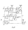
- a CMI signal transmission system which uses the repeater of Fig. 1 comprises a main terminal station 200, repeaters 300A and 300B, and a remote terminal station 400.
- the main terminal station 200 includes a transmission signal generating section 210, an electro-optic converter 220, and a loop-back commanding section 250.
- the section 210 functions to generate a transmission signal by coding a main signal according to a CMI coding rule with some violation caused by a first sub-information signal which is made up of a plurality of different kinds of sub-information which are formatted in a frame.
- the converter 220 serves to convert the transmission signal to an optical signal.
- the main terminal station 200 also receives a transmission signal sent thereto from the terminal station 400 with an opto-electric converter 240 thereof, decodes it with a CMI decoding section 230, and thereby produces a main signal P and a violation signal Q.
- full-duplex communication is held between the main terminal station 200 and the remote terminal station 400.
- the transmission signal generating section 210 adds loop-back command information to the sub-information signal and superposes the resultant signal on the main signal.
- the station 400 on detection of the loop-back command information out of the transmission signal, stops transmission of the own station's main signal and, instead, returns to the main station 200 a signal produced by superposing the own station's sub-information signal on the main signal, which is contained in the received transmission signal.
- the main station 200 checks the violation signal Q for error pulses in order to see the degree of fault occurring in the transmission loop.
- the repeaters 300A and 300B are each constructed in the same manner as the repeater of Fig. 1.
- the station 400 includes an opto-electric converter 410 for converting a transmission signal sent from the repeater 300A to an electric signal, a CMI decoding section 420, a CMI coding section 430, an electro-optic converter 440, a violation signal generating section 450, and a loop-back command information detecting section 460. These sections except for the station 460 may be implemented with the same function blocks as those of the repeater.
- the CMI decoding section 420 in here is a combination of the identifying and regenerating circuit 3, timing circuit 2 and CMI decoding circuit 4 of Fig. 1.
- Figs. 1 and 5 signals which share the same terms as those of Figs. 1 and 5 are designated by like reference numerals for the simplicity of description.
- the CMI decoding section 420 extracts the clock B from the transmission signal and separates a main signal L and a violation signal C.
- the sub-information separating circuit 510A (Fig. 5) in the section 450 separates the sub-information signals DO to D3 and generates error pulses E. Only the own station's sub-information signals D0' to D3' are applied to the sub-information signal multiplexing circuit 510C (Fig. 5) and, via the adder 54, produced as a violation signal J.
- a switch S, and the switch S 2 (Fig. 5) are open to allow the own station's main signal 0 to be fed to the CMI coding section 430.
- the violation signal J is superposed on the own station's main signal O, the composite signal being transmitted via the converter 440. Because the switch S 2 is open, error pulses E associated with the path from the main station 200 to the remote station 400 are not sent out to the path from the station 400 to the station 200.
- the loop-back command information detector 460 detects it out of, among the sub-information signals DO to D3, the one (e.g. signal DO) which is assigned to the loop-back command information, thereby producing a signal T.
- the signal T causes the main signal 0 to be intercepted and the switches S, and S 2 (Fig. 5) to close. Consequently, the main signal L and the violation signal J which includes error pulses E and sub-information signals DO' to D4' are fed to the CMI coder 430. In this instance, the error pulses are not masked by the sub-information signals D0' to D4'.
- the transmission system of Fig. 10 allows the main station 200 to detect errors in the transmission path with remarkably high accuracy since the errors are not masked by any of the repeaters 300A and 300B and the remote station 400.
- error pulses are added in such a manner as not to overlap sub-information superposing bits, no error information can be transmitted without being lost even if sub-information is superposed at a repeater or at a station which is remote from a main station.
Landscapes
- Engineering & Computer Science (AREA)
- Computer Networks & Wireless Communication (AREA)
- Signal Processing (AREA)
- Physics & Mathematics (AREA)
- Spectroscopy & Molecular Physics (AREA)
- Time-Division Multiplex Systems (AREA)
- Dc Digital Transmission (AREA)
Claims (2)
dadurch gekennzeichnet, daß die Störungsanzeigesignal-Erzeugungseinrichtung umfaßt eine Einrichtung zum Erzeugen eines Fehlerpulses, die aus dem Störungssignal einen Zeitschlitz eines Fehlerbits erkennt, das während der Sendung in dem Sendesignal auftritt, eine Einrichtung zum Erzeugen eines zweiten Teilinformationssignals durch Einfügen der Teilinformationssignals der zweiten Station in einen bestimmten Zeitschlitz, eine Fehlerpulsstelle-Veränderungseinrichtung zum Vergleichen des Zeitschlitzes des Fehlerbits und des Zeitschlitzes des zweiten Teilinformationssignals und, wenn die zwei Zeitschlitze nicht miteinander übereinstimmen, zum Erzeugen des Fehlerpulses und, wenn die zwei Zeitschlitze miteinander übereinstimmen, zum Erzeugen eines Fehlerpulses, der gegenüber dem Zeitschlitz des zweiten Teilinformationssignals um eine bestimmte Anzahl von Bits verzögert ist, und eine Einrichtung zum Kombinieren eines Fehlerpulssignals, das von der Fehlerpulsstelle-Veränderungseinrichtung ausgegeben wird, und des zweiten Teilinformationssignals.
Applications Claiming Priority (4)
| Application Number | Priority Date | Filing Date | Title |
|---|---|---|---|
| JP153465/85 | 1985-07-11 | ||
| JP15346585A JPS6214555A (ja) | 1985-07-11 | 1985-07-11 | 誤り重畳回路 |
| JP186539/85 | 1985-08-27 | ||
| JP60186539A JPH0634481B2 (ja) | 1985-08-27 | 1985-08-27 | リモートループバック方式 |
Publications (3)
| Publication Number | Publication Date |
|---|---|
| EP0208558A2 EP0208558A2 (de) | 1987-01-14 |
| EP0208558A3 EP0208558A3 (en) | 1988-01-20 |
| EP0208558B1 true EP0208558B1 (de) | 1990-10-10 |
Family
ID=26482079
Family Applications (1)
| Application Number | Title | Priority Date | Filing Date |
|---|---|---|---|
| EP86305359A Expired EP0208558B1 (de) | 1985-07-11 | 1986-07-11 | Übertragungssystem für CMI-Signale |
Country Status (5)
| Country | Link |
|---|---|
| US (1) | US4783786A (de) |
| EP (1) | EP0208558B1 (de) |
| AU (1) | AU584041B2 (de) |
| CA (1) | CA1258130A (de) |
| DE (1) | DE3674844D1 (de) |
Families Citing this family (6)
| Publication number | Priority date | Publication date | Assignee | Title |
|---|---|---|---|---|
| GB8623610D0 (en) * | 1986-10-01 | 1986-11-05 | Gen Electric | Signalling labelling |
| JPH088561B2 (ja) * | 1988-04-20 | 1996-01-29 | 株式会社日立製作所 | Cmiブロック同期方法 |
| CA2013484A1 (en) * | 1989-06-26 | 1990-12-26 | Can A. Eryaman | Erasure arrangement for an error correction decoder |
| US5113187A (en) * | 1991-03-25 | 1992-05-12 | Nec America, Inc. | CMI encoder circuit |
| JPH07264177A (ja) * | 1994-03-25 | 1995-10-13 | Matsushita Electric Ind Co Ltd | 並列信号光伝送方式 |
| JP3573978B2 (ja) * | 1998-11-10 | 2004-10-06 | 矢崎総業株式会社 | 符号化方法、及び符号化装置 |
Family Cites Families (10)
| Publication number | Priority date | Publication date | Assignee | Title |
|---|---|---|---|---|
| US4006455A (en) * | 1975-10-10 | 1977-02-01 | Texas Instruments Incorporated | Error correction system in a programmable calculator |
| NL7807171A (nl) * | 1978-06-30 | 1980-01-03 | Philips Nv | Ontvanger voor digitale signalen in lijncode. |
| FR2524231A1 (fr) * | 1982-03-29 | 1983-09-30 | Telecommunications Sa | Procede pour transmettre un signal en code hdbn avec un signal binaire auxiliaire, codeur et decodeur selon le procede et systeme de telesurveillance de repeteurs d'une liaison numerique au moyen de tels signaux auxiliaires |
| DE3211977A1 (de) * | 1982-03-31 | 1983-10-06 | Siemens Ag | Betriebsueberwachung von uebertragungsstrecken fuer digitale signale |
| DE3215081A1 (de) * | 1982-04-22 | 1983-11-03 | Siemens AG, 1000 Berlin und 8000 München | System zur uebertragung von informationstelegrammen |
| IT1153596B (it) * | 1982-10-27 | 1987-01-14 | Italtel Spa | Sistema di trasmissione su portante fisico in fibra ottica, di un flusso di dati principale e di un flusso di dati secondario |
| JPS59125144A (ja) * | 1982-12-30 | 1984-07-19 | ソニー株式会社 | デイジタル信号伝送方法 |
| IT8324267A0 (it) * | 1983-12-20 | 1983-12-20 | Italtel Spa | Disposizione circuitale atta a rilevare il tasso di errore in sistemi di trasmissione di tipo numerico. |
| US4642807A (en) * | 1984-12-18 | 1987-02-10 | Motorola, Inc. | Fault tolerant receiver |
| US4677627A (en) * | 1985-06-05 | 1987-06-30 | International Business Machines Corp. | Error correction scheme |
-
1986
- 1986-07-10 CA CA000513450A patent/CA1258130A/en not_active Expired
- 1986-07-11 DE DE8686305359T patent/DE3674844D1/de not_active Expired - Lifetime
- 1986-07-11 AU AU60070/86A patent/AU584041B2/en not_active Ceased
- 1986-07-11 US US06/884,525 patent/US4783786A/en not_active Expired - Fee Related
- 1986-07-11 EP EP86305359A patent/EP0208558B1/de not_active Expired
Also Published As
| Publication number | Publication date |
|---|---|
| DE3674844D1 (de) | 1990-11-15 |
| CA1258130A (en) | 1989-08-01 |
| EP0208558A2 (de) | 1987-01-14 |
| EP0208558A3 (en) | 1988-01-20 |
| US4783786A (en) | 1988-11-08 |
| AU6007086A (en) | 1987-01-15 |
| AU584041B2 (en) | 1989-05-11 |
Similar Documents
| Publication | Publication Date | Title |
|---|---|---|
| US4759018A (en) | Higher order digital transmission system including a multiplexer and a demultiplexer | |
| JPH0124385B2 (de) | ||
| EP0015730B1 (de) | Datenübertragungssystem und Verfahren zum Ubermitteln von Daten über ein Datenübertragungssystem | |
| US3902161A (en) | Digital synchronizer system for remotely synchronizing operation of multiple energy sources and the like | |
| US4849995A (en) | Digital signal transmission system having frame synchronization operation | |
| GB1481849A (en) | Digital code transmission systems | |
| EP0208558B1 (de) | Übertragungssystem für CMI-Signale | |
| EP0243938B1 (de) | Ersatzkanalüberwachungssystem unter Verwendung eines Prüfsignals mit zwei verschiedenen, in einer Zufallsfolge angeordneten n-Bit-Kodemustern | |
| US4551830A (en) | Apparatus for providing loopback of signals where the signals being looped back have an overhead data format which is incompatible with a high speed intermediate carrier overhead format | |
| US4232387A (en) | Data-transmission system using binary split-phase code | |
| US4947394A (en) | Spare channel monitor circuit | |
| EP0206409B1 (de) | Digitales Übertragungssystem höherer Ordnung welches einen Multiplexer und einen Demultiplexer enthält | |
| CA1074029A (en) | Framing circuit for digital signals using evenly spaced alternating framing bits | |
| GB1501351A (en) | Protective relaying system | |
| JPH03270526A (ja) | 差動符号化における誤り波及抑圧方式 | |
| JPH08186554A (ja) | 時分割多重伝送装置および復号化回路 | |
| US5222102A (en) | Digital phased locked loop apparatus for bipolar transmission systems | |
| JP2693831B2 (ja) | 補助信号伝送方式 | |
| JP2767107B2 (ja) | フレームフォーマット変換方法 | |
| CA1106086A (en) | Channel monitoring system | |
| Schneider et al. | A N+ 2 protection switching system for synchronous STM-1 signals and plesiochronous 140 Mbit/s signals by using two carrier technique | |
| JPH02226932A (ja) | Cmi符号の受信装置 | |
| JPH04245733A (ja) | データ伝送方式 | |
| JPH03126340A (ja) | フレーム識別符号伝送方式 | |
| JPS6214555A (ja) | 誤り重畳回路 |
Legal Events
| Date | Code | Title | Description |
|---|---|---|---|
| PUAI | Public reference made under article 153(3) epc to a published international application that has entered the european phase |
Free format text: ORIGINAL CODE: 0009012 |
|
| 17P | Request for examination filed |
Effective date: 19860722 |
|
| AK | Designated contracting states |
Kind code of ref document: A2 Designated state(s): DE GB SE |
|
| PUAL | Search report despatched |
Free format text: ORIGINAL CODE: 0009013 |
|
| AK | Designated contracting states |
Kind code of ref document: A3 Designated state(s): DE GB SE |
|
| 17Q | First examination report despatched |
Effective date: 19891117 |
|
| GRAA | (expected) grant |
Free format text: ORIGINAL CODE: 0009210 |
|
| AK | Designated contracting states |
Kind code of ref document: B1 Designated state(s): DE GB SE |
|
| REF | Corresponds to: |
Ref document number: 3674844 Country of ref document: DE Date of ref document: 19901115 |
|
| PGFP | Annual fee paid to national office [announced via postgrant information from national office to epo] |
Ref country code: SE Payment date: 19910626 Year of fee payment: 6 |
|
| PGFP | Annual fee paid to national office [announced via postgrant information from national office to epo] |
Ref country code: GB Payment date: 19910703 Year of fee payment: 6 |
|
| PLBE | No opposition filed within time limit |
Free format text: ORIGINAL CODE: 0009261 |
|
| STAA | Information on the status of an ep patent application or granted ep patent |
Free format text: STATUS: NO OPPOSITION FILED WITHIN TIME LIMIT |
|
| PGFP | Annual fee paid to national office [announced via postgrant information from national office to epo] |
Ref country code: DE Payment date: 19910927 Year of fee payment: 6 |
|
| 26N | No opposition filed | ||
| PG25 | Lapsed in a contracting state [announced via postgrant information from national office to epo] |
Ref country code: GB Effective date: 19920711 |
|
| PG25 | Lapsed in a contracting state [announced via postgrant information from national office to epo] |
Ref country code: SE Effective date: 19920712 |
|
| GBPC | Gb: european patent ceased through non-payment of renewal fee |
Effective date: 19920711 |
|
| PG25 | Lapsed in a contracting state [announced via postgrant information from national office to epo] |
Ref country code: DE Effective date: 19930401 |
|
| EUG | Se: european patent has lapsed |
Ref document number: 86305359.1 Effective date: 19930204 |