EP0210861A2 - Dispositif de détection de mouvement dans une image de télévision - Google Patents
Dispositif de détection de mouvement dans une image de télévision Download PDFInfo
- Publication number
- EP0210861A2 EP0210861A2 EP86305792A EP86305792A EP0210861A2 EP 0210861 A2 EP0210861 A2 EP 0210861A2 EP 86305792 A EP86305792 A EP 86305792A EP 86305792 A EP86305792 A EP 86305792A EP 0210861 A2 EP0210861 A2 EP 0210861A2
- Authority
- EP
- European Patent Office
- Prior art keywords
- data
- difference data
- frame
- circuit
- output
- Prior art date
- Legal status (The legal status is an assumption and is not a legal conclusion. Google has not performed a legal analysis and makes no representation as to the accuracy of the status listed.)
- Granted
Links
Images




Classifications
-
- H—ELECTRICITY
- H04—ELECTRIC COMMUNICATION TECHNIQUE
- H04N—PICTORIAL COMMUNICATION, e.g. TELEVISION
- H04N5/00—Details of television systems
- H04N5/14—Picture signal circuitry for video frequency region
- H04N5/144—Movement detection
-
- G—PHYSICS
- G06—COMPUTING OR CALCULATING; COUNTING
- G06T—IMAGE DATA PROCESSING OR GENERATION, IN GENERAL
- G06T7/00—Image analysis
- G06T7/20—Analysis of motion
- G06T7/254—Analysis of motion involving subtraction of images
Definitions
- This invention relates to apparatus for detecting television image movement.
- Such apparatus is particularly, but not exclusively, suitable for use in a video signal standards conversion circuit.
- a block matching method has been used to detect movement vectors each representing the amount and direction of movement of a television image from one frame to the next in response to frame difference data between present frame data and previous frame data.
- a video signal is divided into a number of segmental areas or blocks for each frame.
- the frame difference data are produced for each of the segmental areas by calculating differences in the positions or coordinates of picture elements representing corresponding segmental areas of successive frames. These calculations are effected by a digital computer operable in accordance with a program stored in the computer memory.
- the frame difference data are produced by calculating differences in the position or coordinates of the pixel representative of a segmental area of one frame relative to the position or coordinates of the respective picture element of the corresponding segmental area of the subsequent frame.
- an apparatus for detecting a movement vector indicating an amount and direction of a movement in a picture defined by a television signal made up of successive intervals comprising:
- apparatus for detecting movement of a television image in response to frame difference data corresponding to a difference between present frame data and previous frame data, and in which a video signal is divided into a plurality of segmental areas for each frame and each segmental area is represented by a representative picture element
- the apparatus comprising: means for producing frame difference data for each of the segmental areas in accordance with differences in the positions of said representative picture element of a respective segmental area in a present frame and a previous frame, respectively;
- a video signal is divided into a plurality of segmental areas for each frame, a pixel is selected to represent each of the segmental areas, frame difference data are produced for each of the segmental areas by calculating differences in the position or coordinates of a pixel representative of a segmental area of a previous frame in respect to the position or coordinates of the respective picture element of the corresponding segmental area of a present frame, and means are provided to omit from the frame difference data and the calculated differences which are smaller than a predetermined magnitude. This is effective to improve the movement vector detection accuracy.
- the movement vector detecting circuit of Figure 1 includes an input terminal 1 to which a digital video signal is applied.
- the digital video signal is supplied from the input terminal 1 to one input of a subtracter 2 and also to a representative pixel extraction circuit 3.
- the extraction circuit 3 extracts a pixel or point representative of each of the segmental areas of one frame and produces pixel data indicative of the position or coordinates of the extracted representative pixel.
- the pixel data are fed from the extraction circuit 3 to, and stored in, a representative pixel memory 4.
- the stored data are read out of the representative pixel memory 4 and applied at appropriate times to another input of the subtracter 2.
- the data fed from the memory 4 to the subtracter 2 are previous frame data, and the digital video signal applied directly from the input terminal 1 to the substracter 2 is present frame data.
- the subtracter 2 produces frame difference data ⁇ F by calculating differences between the position or coordinates of the pixel representative of a segmental area of the previous frame and the position or coordinates of the respective picture element of the corresponding segmental area of the subsequent or present frame.
- the frame difference data ⁇ F are converted by a converter 5 into data
- ⁇ Ft are fed to a summation circuit 6 which adds or sums the absolute values of the differences for the respective picture elements of each of the segmental areas to provide frame difference summation data ⁇ ( ⁇ Fl.
- FI are fed to a minimum data detection circuit 7.
- the minimum data detection circuit 7 receives frame difference summation data ⁇
- Figure 3 depicts the frame difference summation data ⁇
- the minimum frame difference summation data corresponds to a zero movement vector. This means that the apparatus of Figure 1 indicates that the object remains at rest in spite of the fact that the object moves, as indicated at 9 in Figure 3.
- a video signal to be received by an embodiment of movement vector detection circuit in accordance with the present invention is divided into a plurality of segmental video signal areas for each frame.
- Eacn segmental area includes sixty-three picture elements, that is, seven lines each carrying nine picture elements, as shown in Figure 7.
- Each segmental area is represented by the position or coordinates (x, y) of a representative pixel placed at the centre of the segmental area, as designated by the character X in Figure 7.
- the segmental areas may be defined partially to overlap each other.
- an embodiment of movement vector detection circuit includes an input terminal 11 to which a digital video signal is applied.
- the digital video signal is supplied from the input terminal 11 directly to one input of a subtracter 12, and also to a representative pixel extraction circuit 13.
- the extraction circuit 13 extracts a pixel or point representative of each of the segmental areas of one frame and produces pixel data indicative of the position or coordinates of the extracted representative pixel.
- Such pixel data are read into, and stored in a representative pixel memory 14.
- the stored data are read out of the memory 14 and applied, as previous frame data, to another input of the subtracter 12.
- the digital video signal applied directly from the input terminal 11 to the first mentioned input of the subtracter 12 carries present frame data which relate to the positions or coordinates of respective picture elements included in the corresponding segmental area of the present frame. Consequently, the subtracter 12 produces frame difference data A F by calculating differences in the position or coordinates of the pixel representative of the segmental area of the previous frame from the position or coordinates of the respective picture element of the corresponding segmental area of the present frame.
- the frame difference data ⁇ F are converted by a converter 15 into data
- the absolute values of frame difference data (6 F( are fed to a limiter circuit 16 which limits the values of the differences of the data l6 Ft below a predetermined value.
- the output of the limiter circuit 16 is applied to a minimum data detector circuit 20.
- the detector circuit 20 detects the position or address of the picture element for which the absolute value of the frame difference data
- the output of the detector circuit 20 is applied to a decision circuit 21 which determines whether or not the detected picture element is in a small vector region enclosed by the - broken line in Figure 7. If the picture element is in that small vector region, then it means that the movement vector will be too small to be reliably considered and the decision circuit 21 produces a low level control signal. Otherwise, the decision circuit 21 produces a high level control signal which is applied to a switching circuit 18.
- the switching circuit 18 has a first input terminal 19A connected through a delay circuit 17 to the limiter circuit 16, a second input terminal 198 connected to earth or a source of zero data, and an output terminal 19C connected to a summation circuit 22.
- the switching circuit 18 responds to a high level control signal from the decision circuit 21 to cause engagement of the terminals 19A and 19C, and thereby permit the summation circuit 22 to receive the data
- the delay circuit 17 delays the signal from the limiter circuit 16 to the terminal 19A, so as to compensate for the inherent delay in the time of arrival of the control signal at the switching circuit 18.
- the summation circuit 22 sums the absolute values of the data differences for the picture elements of each of the segmental areas to provide frame difference summation data ⁇
- the summation circuit 22 preferably includes a digital integrator for summing the data fed from the terminal 19C to produce frame difference summation data ⁇
- the switching circuit 18 responds to a low level control signal from the decision circuit 21 to cause engagement of the terminals 19B and 19C, and thereby connect the summation circuit 22 to the zero data source.
- are fed from the summation circuit 22 to a minimum data detector circuit 23.
- the minimum data detector circuit 23 receives the frame difference summation data ⁇
- a counter 27 also receives the control signal from the decision circuit 21, and counts the number of occurrences of a low level control signal therefrom for each period during which all of the picture elements included in one segmental area are processed.
- the content of the counter 27 represents the number of frame difference data
- a comparator circuit 29 compares the content of the counter 27 with a reference value fed thereto from a reference generator 28.
- the reference value provided by the reference generator 28 may correspond to 80 percent of the number of the picture elements included in one segmental area. When the content of the counter 27 exceeds such reference value, the comparator circuit 29 supplies a low level control signal to a switching circuit 24.
- the switching circuit 24 has a first input terminal 25A connected to the output of the minimum data detector circuit 23, a second input terminal 25B connected to earth or a source of zero data, and an output terminal 25C connected to an output terminal 26.
- the switching circuit 24 responds to a high level control signal from the comparator circuit 29 to provide a connection between the terminals 25A and 25C so that a signal indicative of the movement vector detected in the minimum data detector circuit 23 appears at the output terminal 26.
- the switching circuit 24 responds to a low level control signal from the comparator circuit 29 to provide a connection between the terminals 25B and 25C, so that a zero movement vector appears at the output terminal 26.
- circuit shown in Figure 6 exhibits generation of an unreliable movement vector by zeroing the detected movement vector when a relatively great number of frame difference data are omitted from the data used in detecting a movement vector.
- the switching circuit 18 forms, in effect, gating means for the data difference (6 Fl so as to supply such data difference
- the decision circuit 21 provides a high level control signal to the switching circuit 18 for supplying data difference (0 Fi to the summation circuit or accumulating means 22 only when the detector circuit 20 and the decision circuit 21 cooperate to indicate that the segmental area of the frame being considered corresponds to a moving object, and not a stationary background portion, in the television image.
- the minimum frame difference summation data correspond to movement of an object, as shown in Figure 8, even when the object moves against a distinct background which changes substantially across the television image. Therefore, this embodiment makes it possible to detect movement vectors with greater accuracy.
- the apparatus of Figure 9 further includes a gate circuit 56 through which the data
- the gate circuit 56 supplies a predetermined value, for example, a quantization level 64, to the summation circuit 60 regardless of the value of the data 16 Ft fed thereto from the converter 15 whenever the picture element is determined to be in a non-movement range, that is, corresponds to a stationary portion of the background of the television image, as described later in detail.
- This determination is made by a circuit including a frame memory 57, a subtracter 58, and a threshold circuit 59.
- the frame memory 57 receives the digital video signal directly from the input terminal 11 and provides previous frame data which relate to the positions or coordinates of the respective picture elements of a segmental area included in the previous frame.
- the previous frame data are fed to the subtracter 58 which also receives present frame data directly from the input terminal 11.
- the present frame data relate to the positions or coordinates of the respective picture elements of the corresponding segmental area included in the present frame.
- the subtracter 58 produces frame difference data representing the difference between the present frame data and the previous frame data by calculating differences between the positions or coordinates of the picture elements of the segmental area of the previous frame and the positions or coordinates of the respective picture elements of the corresponding segmental area of the present frame.
- the subtracter 58 produces a zero output or difference signal, it is established thereby that the corresponding picture element remains at rest, that is, part of a stationary background portion of the television image.
- the difference signal from the subtracter 58 is not zero when a picture element remains at rest.
- the output of the subtracter 58 is coupled to the threshold circuit 59 which compares the difference signal with a preferably adjustable threshold value for determining the non-movement range, and which has its output connected to the gate circuit 56 as a gating signal for the latter.
- the threshold circuit 59 produces a low level decision signal or output to cause the gate circuit 56 to close and to supply the predetermined value corresponding to the quantizing level 64 to the summation circuit 60 when the difference signal from the subtracter 58 is less than the adjustable threshold value. Otherwise, the threshold circuit 59 produces a high level decision signal or output to open the gate circuit 56 for passing the data (L1 Fi from the converter 15 to the summation circuit 60.
- the output of the threshold circuit 59 is also coupled to a counter 63 which counts the number of occurrences of a low level decision signal at the output of the threshold circuit 59. The count of the counter 63 represents the number of the data
- a comparator circuit 66 compares the content of the counter 63 with a reference value fed thereto from a reference generator 65.
- the reference value from the reference generator 65 may correspond to 80 percent of the number of picture elements included in one segmental area.
- the comparator circuit 66 produces a control signal for zeroing a movement vector, as hereinafter described.
- the summation circuit 60 preferably includes a digital integrator for summing the data fed from the gate circuit 56 to produce frame difference summation data ⁇
- the summation circuit 60 also includes a memory having a number of memory sections or addresses corresponding to the number of the segmental areas included in one field for storing the successively produced frame difference summation data in the respective memory sections.
- are fed from the summation circuit 60 to a minimum data detector circuit 61.
- the minimum data detector circuit 61 receives frame difference summation data ⁇
- the output of the threshold circuit 59 which controls the gate circuit 56 is effective to indicate whether the segmental area of the frame being considered is part of stationary background portion of the television image or, is part of a moving object.
- the gate circuit 56 is opened by its control signal from threshold circuit 59 for passing the data difference
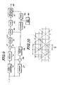
- Figure 10 shows a pattern in which the picture elements of a segmental area may be arranged to improve the capacity for detecting movement of television images having vertical strips or other patterns having high spatial frequencies.
- a pixel representative of a first segmental area and a pixel representative of a second segmental area just below or above the first segmental area are offset X/2 in the horizontal direction to provide a checkerboard-like pattern, in which X is the horizontal distance between two representative pixels adjacent to each other in the horizontal direction.
- the segmental areas may partially overlap each other.
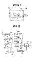
- Figure 11 illustrates an image comprising a car that starts crossing a distinct background.
- a conventional movement vector detecting apparatus no movement vector is detected in the region 718 and movement of the car cannot be detected until it has, at least to some extent, entered the region 71C. Since a low-pass filter is normally used to filter the video signal for suppressing sudden image changes and discontinuous movements, substantial time is required until the movement is corrected after a movement is detected in the region 71C. For these reasons, in the reproduced picture, the car appears to move in an unnatural manner, that is, as if it starts running after the application of braking.
- FIG. 12 shows a television standards conversion system to which an embodiment of movement vector detecting apparatus according to the invention can advantageously be applied.
- the system of Figure 12 includes an input terminal 71 to which a high definition television (HDTV) signal is applied.
- the HDTV signal is supplied from the input terminal 71 to three gate circuits 72A, 72B and 72C.
- the gate circuit 72A serves to pass picture elements included in the left-hand region 71A in Figure 11, and the gate circuits 72B and 72C serve to pass picture elements included in the righthand region 71B and the centre region 71C, respectively.
- a pulse generator 73 triggered by a suitable sync signal applied to a terminal 74, provides suitably timed gating signals to the gate circuits 72A, 72B and 72C.
- the centre region 71C overlaps the output image, and the left-hand and righthand regions 71a and 71B do not overlap the output image, that is, are outside the desired output image.
- the outputs of the gate circuits 72A, 72B and 72C are coupled to movement vector detecting circuits 75A, 75B and 75C, respectively.
- Each of the movement vector detecting circuits 75A, 75B and 75C is substantially the same in structure as that described above in connection with Figure 6 or Figure 9.
- the movement vector detecting circuit 75A serves to detect a movement vector Va corresponding to movement of the car in the left-hand region 71A
- the movement vector detecting circuit 75B serves to detect a movement vector Vb corresponding to movement of the car in the righthand region 71B
- the movement vector detecting circuit 75C serves to detect a movement vector Vc corresponding to movement of the car in the centre region 71C ( Figure 11).
- the movement vectors Va, Vb and Vc are all supplied to a decision circuit 76.
- the movement vector Vc is also supplied to a digital low-pass filter 77 which is effective to suppress sudden movement vector changes so as to minimize large jumping and discontinuous movements.
- the digital low-pass filter 77 is of a known type that changes its characteristics in a manner to retard the time when the movement vector falls, or to advance the time when the movement vector rises In accordance with a control signal fed thereto from the decision circuit 76.
- the decision circuit 76 produces the control signal for the digital low-pass filter 77 on the basis of the movement vectors Va, Vb and Vc detected for the regions 71A, 71B and 71C in Figure 11.
- the control signal for the digital low-pass filter 77 is generated when the object moves out of the output image or when the object moves into the output image. The type of control signal generated in the cases i to iv listed in the table below is described thereafter.
- each sign (/) designates a movement vector that is not considered in the decision circuit 76.
- the object (car) moves out of the output image to the left in case i, and the object moves out of the output image to the right in case ii.
- the decision circuit 76 provides a control signal which is effective to cause the digital low-pass filter 77 to retard the time when the movement vector falls, so as to maintain the magnitude of the movement vector in the centre region 71C ( Figure 11). This is effective to suppress the tendency to decrease the magnitude of the movement vector when the object moves out of the output image, and thereby eliminates the apparent decrease in the speed of movement of the object as it moves out of the output image.
- the object moves into the output image from the right in case iii of the above table, and the object moves into the output image from the left in the case iv.
- the decision circuit 76 provides a control signal which causes the digital low-pass filter 77 to advance the time when the movement vector rises. Therefore, the movement vector in the region 71C can rise as soon as the object arrives at an end of the output image in entering the latter. In cases other than those listed in the above table, the characteristic of the digital low-pass filter 77 is maintained unchanged.
- the movement vector provided at an output terminal 78 may be used for effecting movement correction in a field number conversion circuit of a television standards conversion system, as described below.
- embodiments of the invention may be applied to field number conversion when effecting standards conversion from a HDTV (high definition television) system employing 1125 lines per frame and sixty fields per second, to a PAL TV (phase alternation by line television) system employing 625 lines per frame and fifty fields per second.
- HDTV high definition television
- PAL TV phase alternation by line television
- the television standards conversion system of Figure 13 is shown to include an input terminal 121 which receives a luminance signal included in an HDTV signal. Such luminance signal is applied through a low-pass filter 122 to an analog-to-digital (A/D) converter 123 which converts it into a corresponding digital signal. The digital signal is applied from the A/D converter 123 to a preprocessing circuit 124.
- A/D analog-to-digital
- the preprocessing circuit 124 utilizes a digital frequency conversion technique to convert the line number from 1125 lines to 625 lines, and also a non-interlace technique to provide, from each field of the HDTV signal simultaneously formed first and second fields each consisting of 625 lines and each displaying the same video image, but with the video images of the first and second fields being offset by 0.5 line distance. Moreover, the first and second fields produced from each field of the HDTV signal each occur at the rate of sixty per second.
- the preprocessing circuit 124 simultaneously provides a first digital video signal VD1 made up of only the first field and which contains 625 lines per frame and sixty frames per second, and a second digital video signal VD2 made up of only the second field and which contains 625 lines per frame and sixty frames per second.
- the first digital video signal VD1 is applied to a movement vector detection circuit 125, and also to a first field number conversion circuit 131.
- the second digital video signal VD2 is applied to a second field number conversion circuit 132 which is substantially the same in structure as the first field number conversion circuit 131.
- the movement vector detection circuit 125 detects movement vectors in response to the first digital video signal VD1.
- the non-interlace technique used in the preprocessing circuit 124 permits the movement vector detection circuit 125 to detect movement vectors at time intervals of 1/60 of a second. This is effective to improve the accuracy of detection of movement vectors and facilitate formation of interpolation signals.
- the movement vector detection circuit 125 produces field difference data between present field data and previous field data substantially in the same manner as described in connection with Figure 6 or Figure 9.
- the first field number conversion circuit 131 provides a digital video signal containing a first 625-lines per frame/50-frames per second field to one input of a switching circuit 141 which, at another input thereof, receives a second digital video signal containing a second 625-lines per frame/50-frames per second field and being provided by the second field number conversion circuit 132.
- the switching circuit 141 also receives a suitably generated control signal Sc which inverts at time intervals of 1/50 of a second so that the switching circuit 141 is changed-over at that rate and provides, at its output, a 625-lines per frame/50-fields per second digital luminance signal.
- This digital luminance signal is then applied to a digital-to-analog (D/A) converter 142 which converts it into a corresponding analog signal.
- the analog signal is applied from the D/A converter 142 through a low-pass filter 143 to a PAL colour encoder 144.
- the PAL colour encoder 144 receives additional inputs including red and blue colour difference signals R-Y and B-Y which have been each subjected to line and field-number conversion similar to that described for the luminance signal Y.
- the PAL colour encoder 144 supplies a composite colour television signal according to the PAL standard to an output terminal 145 which is for connection to a PAL colour television monitor or receiver.
- the first field number conversion circuit 131 includes a field memory 133, a movement correction circuit 134, a linear approximation circuit 135, a switching circuit 136, an error processing circuit 137, and a memory 138.
- the field memory 133 receives the first digital video signal VD1 from the preprocessing circuit 124 and provides, at its output, a digital video signal indicative of previous field data.
- the movement correction circuit 134 receives the first digital video signal VD1 indicative of present field data directly from the preprocessing circuit 124, the digital video signal indicative of previous field data from the field memory 133, and a movement vector indication signal from the movement vector detection circuit 125.
- the movement correction circuit 134 operates to reduce the field number by correcting movement of a moving object. This operation will be described in greater detail with reference to Figure 14, in which Fl, F2, F3, F4, F5 and F6 indicate six image fields which appear in this sequence to represent uniform movement of a triangularly-shaped object from the left to the right. In each constant time interval of 1/60 of a second, the object moves a constant distance A which corresponds to the movement vector detected in the movement vector detection circuit 125. In the illustrated case, the six fields Fl to F6 are converted into five fields fl to f5.
- the field number can be reduced from six to five by shifting the image in the field Fl a distance (1/5)A to provide a shifted image in the field fl, shifting the image in the field F2 a distance (2/5)A to provide a shifted image in the field f2, shifting the image in the field F3 a distance (3/5)A to provide a shifted image in the field f3, shifting the image in the field F4 a distance (4/5)A to provide a shifted image in the field f4, and shifting the image in the field F5 a distance A to provide a shifted image in the field f5.
- the image shifting operation can be realized by suitable memory address control.
- the movement correction circuit 134 can achieve complete field number conversion for images obtained during panning or tilting of a television camera if the movement vectors can be detected with high accuracy, problems could occur for images having objects moving simultaneously in various ways.
- FIG. 15 Another way in which field number conversion can be effected by the movement correction circuit 134 is illustrated in Figure 15, in which Fl, F2, F3, F4, F5 and F6 again indicate six image fields which appear in this sequence to represent uniform movement of an object from left to the right.
- the object moves a constant distance A which corresponds to the movement vector detected in the movement vector detection circuit 125.
- the six fields F1 to F6 are converted into five fields fl to f5 using previous and present field data.
- the field number can be reduced from six to five by halving the output signal corresponding to the sum of an image resulting from the shifting of the image in the field Fl by a distance (1/5)A, and an -image resulting from the shifting of the imag in the field F2, by a distance(-4/5)A to provide a shifted image in the field fl; halving the output signal corresponding to the sum of an image resulting from the shifting of the image in the field F2 by a distance (2/5)A and an image resulting from the shifting of the image in the field F3 by a distance (-3/5)A to provide a shifted image in the field f2; halving the output signal corresponding to the sum of an image resulting from the shifting of the image in the field F3 by a distance (3/5)A and an image resulting from the shifting of the image in the field F4 by a distance (-2/5)A to provide a shifted image in the field f3; halving the output signal corresponding to the sum of an image resulting from
- n is an integer from 1 to 5
- these images are desirably added, and the sum then halved, for equalizing the signal-to-noise (S/N) ratio relating to random noises produced during linear approximation and the S/N ratio relating to the random noises produced during movement correction, and also for vignetting the image when the movement vector is erroneously detected.
- S/N signal-to-noise
- the linear approximation circuit 135 operates to reduce the field number by calculating a weighted average of the images in two successive fields to which predetermined wieghts are respectively assigned. This operation will be described in greater detail with reference to Figure 16 in which Fl, F2, F3, F4, F5 and F6 indicate six image fields which appear in this sequence at time intervals of 1/60 of a second.
- the smaller triangle in each field of Figure 16 indicates a moving object.
- the six fields Fl to F6 are converted by a weight (4/5) and the image in field F2 multiplied by a weight (1/5) are combined or averaged to provide an image in the field fl.
- Each triangle indicated in broken lines is the image in the subsequent field.
- the image in the field F2 multiplied by a weight (3/5) and the image in the field F3 multiplied by a weight (2/5) are combined to provide an image in the field f2.
- the image in the field F3 multiplied by a weight (2/5) and the image in the field F4 multiplied by a weight (3/5) are combined to provide an image in the field f3.
- the image in the field F4 multiplied by a weight (1/5) and the image in the field F5 multiplied by a weight (4/5) are combined to provide an image in the field f4.
- the image in the field F6 is used as the image in the field f5.
- linear approximation has a tendency to double or vignette a moving image, it can provide a better stationary image than movement correction.
- the error processing circuit 137 will now be described with reference to Figure 17 in which an input terminal 151 receives a digital video signal corresponding to the previous field Fl ( Figure 18), and an input terminal 152 receives a digital video signal corresponding to the present field F2 ( Figure 18).
- the digital video signals are applied from the terminals 151 and 152 to a subtracter 153 which produces field difference data FL corresponding to the difference between the previous and present field data by calculating differences in the positions or coordinates of the picture elements of the segmental area of the previous field fro the coordinates of the respective picture elements of the corresponding segmental area of the present field.
- the error processing circuit 137 also includes an input terminal 154 receiving a signal corresponding to the field fll ( Figure 18) and an input terminal 155 receiving a signal corresponding to the field fl2 ( Figure 18).
- the image in the previous field Fl is shifted a distance (2/5)A to provide an image in the field fll.
- the image in the present field F2 is shifted a distance (-3/5)A to provide an image in the field f12.
- These signals are supplied to a subtracter 156 which produces field difference data ⁇ f by calculating differences in the positions or coordinates of the picture elements of the segmental area of the field fll relative to the coordinates of the respective picture elements of the corresponding segmental area of field f12.
- the field difference data AFL and the field difference data ⁇ f are compared in a comparator circuit 157.
- the images of the fields fll and f12 are the same in respect to the position of the moving triangularly-shaped object and, thus, the field difference data ⁇ f have no moving portion.
- the images of the fields Fl and F2 are the same in respect to the position of the stationary circular portion. Consequently, it can be determined that movement correction by circuit 134 is reliable when A FL is greater than ⁇ f and that the movement correction is not reliable when AFL is less than ⁇ f.
- the comparator circuit 157 produces a high level signal when AFL is greater than Af and a low level signal when ⁇ FL is less than ⁇ f.
- the output of the comparator circuit 157 is supplied to a majority logic circuit 158 which provides a decision for each of the segmental areas. More particularly, when the number of occurrences of a high level signal at the output of the comparator circuit 157 is greater than the number of occurrences of a low level signal at the output of the comparator circuit 157 for a segmental area, the majority logic circuit 158 provides a high level signal at an output terminal 159. Otherwise, the majority logic circuit 158 produces a low level signal at the output terminal 159 which is coupled to the switching circuit 136 in Figure 13.
- the switching circuit 136 connects the movement correction circuit 134 to the memory 138 in response to a high level control signal from the output terminal 159 to the error processing circuit 137.
- the switching circuit 136 is changed-over so as to connect the linear approximation circuit 135 to the memory 138 in response to a low level control signal from the error processing circuit 137. Therefore, movement correction by the error correction circuit 134 is employed when a moving image is involved, and linear approximation by the linear approximating circuit 135 is employed when a stationary image is being processed.
Landscapes
- Engineering & Computer Science (AREA)
- Multimedia (AREA)
- Signal Processing (AREA)
- Physics & Mathematics (AREA)
- General Physics & Mathematics (AREA)
- Theoretical Computer Science (AREA)
- Computer Vision & Pattern Recognition (AREA)
- Testing, Inspecting, Measuring Of Stereoscopic Televisions And Televisions (AREA)
- Image Analysis (AREA)
- Details Of Television Systems (AREA)
- Closed-Circuit Television Systems (AREA)
- Television Systems (AREA)
- Compression Or Coding Systems Of Tv Signals (AREA)
Priority Applications (1)
| Application Number | Priority Date | Filing Date | Title |
|---|---|---|---|
| AT86305792T ATE78650T1 (de) | 1985-07-26 | 1986-07-28 | Geraet zur feststellung von bewegung im fernsehbild. |
Applications Claiming Priority (8)
| Application Number | Priority Date | Filing Date | Title |
|---|---|---|---|
| JP60165072A JPH0783469B2 (ja) | 1985-07-26 | 1985-07-26 | 動きベクトル検出装置 |
| JP60165071A JPH0720238B2 (ja) | 1985-07-26 | 1985-07-26 | 動きベクトル検出回路 |
| JP60165074A JPH0683436B2 (ja) | 1985-07-26 | 1985-07-26 | 動きベクトル検出方法 |
| JP165074/85 | 1985-07-26 | ||
| JP165073/85 | 1985-07-26 | ||
| JP165072/85 | 1985-07-26 | ||
| JP165071/85 | 1985-07-26 | ||
| JP60165073A JPH0720237B2 (ja) | 1985-07-26 | 1985-07-26 | 動きベクトル検出回路 |
Publications (3)
| Publication Number | Publication Date |
|---|---|
| EP0210861A2 true EP0210861A2 (fr) | 1987-02-04 |
| EP0210861A3 EP0210861A3 (en) | 1988-11-02 |
| EP0210861B1 EP0210861B1 (fr) | 1992-07-22 |
Family
ID=27473971
Family Applications (1)
| Application Number | Title | Priority Date | Filing Date |
|---|---|---|---|
| EP86305792A Expired - Lifetime EP0210861B1 (fr) | 1985-07-26 | 1986-07-28 | Dispositif de détection de mouvement dans une image de télévision |
Country Status (5)
| Country | Link |
|---|---|
| US (1) | US4779131A (fr) |
| EP (1) | EP0210861B1 (fr) |
| AT (1) | ATE78650T1 (fr) |
| AU (1) | AU585040B2 (fr) |
| DE (1) | DE3686104T2 (fr) |
Cited By (5)
| Publication number | Priority date | Publication date | Assignee | Title |
|---|---|---|---|---|
| GB2221367B (en) * | 1988-06-22 | 1992-11-11 | British Broadcasting Corp | Bandwidth reduction system for television |
| US5173770A (en) * | 1990-04-27 | 1992-12-22 | Canon Kabushiki Kaisha | Movement vector detection device |
| EP0415737A3 (en) * | 1989-08-29 | 1993-11-03 | Sony Corp | Motion detecting circuits for video images |
| GB2271036A (en) * | 1992-09-23 | 1994-03-30 | Philips Electronics Nv | Image motion estimation using a composite digital input |
| DE4327779C1 (de) * | 1993-08-18 | 1994-12-08 | Siemens Ag | Verfahren und Schaltungsanordnung für ein Fernsehgerät zur Verminderung des Flimmerns |
Families Citing this family (23)
| Publication number | Priority date | Publication date | Assignee | Title |
|---|---|---|---|---|
| US5029001A (en) * | 1986-08-14 | 1991-07-02 | Sony Corporation | NTSC compatible TV signal transmitting system for improving vertical resolution |
| GB8627787D0 (en) * | 1986-11-20 | 1986-12-17 | British Telecomm | Pattern processing |
| FR2613892A1 (fr) * | 1987-04-10 | 1988-10-14 | Labo Electronique Physique | Procede et dispositif d'estimation de mouvement dans une sequence d'images |
| US5012270A (en) * | 1988-03-10 | 1991-04-30 | Canon Kabushiki Kaisha | Image shake detecting device |
| US4933757A (en) * | 1988-08-20 | 1990-06-12 | Olympus Optical Co., Ltd. | Electronic endoscope apparatus provided with a movement detecting means |
| JP2828105B2 (ja) * | 1988-10-27 | 1998-11-25 | オリンパス光学工業株式会社 | 動き検出回路 |
| US5134472A (en) * | 1989-02-08 | 1992-07-28 | Kabushiki Kaisha Toshiba | Moving object detection apparatus and method |
| US4958378A (en) * | 1989-04-26 | 1990-09-18 | Sun Microsystems, Inc. | Method and apparatus for detecting changes in raster data |
| DK0461209T3 (fr) * | 1989-10-20 | 1997-02-17 | Snell & Wilcox Ltd | |
| JP2576771B2 (ja) * | 1993-09-28 | 1997-01-29 | 日本電気株式会社 | 動き補償予測装置 |
| JP3606597B2 (ja) * | 1994-01-21 | 2005-01-05 | ソニー株式会社 | 動きベクトル検出装置 |
| US5561477A (en) * | 1994-10-26 | 1996-10-01 | Thomson Consumer Electronics, Inc. | System for coding a video signal in the presence of an image intensity gradient |
| US5500689A (en) * | 1994-10-26 | 1996-03-19 | Thomson Consumer Electronics, Inc. | System for detecting a video signal image intensity gradient |
| US6101276A (en) * | 1996-06-21 | 2000-08-08 | Compaq Computer Corporation | Method and apparatus for performing two pass quality video compression through pipelining and buffer management |
| US6496228B1 (en) * | 1997-06-02 | 2002-12-17 | Koninklijke Philips Electronics N.V. | Significant scene detection and frame filtering for a visual indexing system using dynamic thresholds |
| US6359658B1 (en) * | 2000-03-06 | 2002-03-19 | Philips Electronics North America Corporation | Subjective noise measurement on active video signal |
| CN1606758A (zh) * | 2000-08-31 | 2005-04-13 | 雷泰克公司 | 传感器和成像系统 |
| US7321699B2 (en) | 2002-09-06 | 2008-01-22 | Rytec Corporation | Signal intensity range transformation apparatus and method |
| JP4489033B2 (ja) * | 2005-03-25 | 2010-06-23 | 三洋電機株式会社 | フレームレート変換装置、パン・チルト判定装置および映像装置 |
| JP4799330B2 (ja) * | 2006-09-08 | 2011-10-26 | 株式会社東芝 | フレーム補間回路、フレーム補間方法、表示装置 |
| US8432495B2 (en) * | 2006-09-15 | 2013-04-30 | Panasonic Corporation | Video processor and video processing method |
| JP5029543B2 (ja) * | 2008-09-09 | 2012-09-19 | 富士通株式会社 | 符号化装置および符号化プログラム |
| JP5424852B2 (ja) * | 2009-12-17 | 2014-02-26 | キヤノン株式会社 | 映像情報処理方法及びその装置 |
Citations (2)
| Publication number | Priority date | Publication date | Assignee | Title |
|---|---|---|---|---|
| JPS59226604A (ja) | 1983-06-03 | 1984-12-19 | 株式会社日立製作所 | ガス絶縁開閉装置 |
| EP0180446A2 (fr) | 1984-10-27 | 1986-05-07 | Sony Corporation | Procédés pour la détection du mouvement dans des images de télévision |
Family Cites Families (13)
| Publication number | Priority date | Publication date | Assignee | Title |
|---|---|---|---|---|
| US3932703A (en) * | 1968-05-27 | 1976-01-13 | Bolsey Emil J | Image motion and change transducers and systems controlled thereby |
| JPS5240911A (en) * | 1975-09-27 | 1977-03-30 | Kokusai Denshin Denwa Co Ltd <Kdd> | Line number conversion system of tv signal |
| US4240101A (en) * | 1976-10-14 | 1980-12-16 | Micro Consultants, Limited | Television standards conversion |
| US4218703A (en) * | 1979-03-16 | 1980-08-19 | Bell Telephone Laboratories, Incorporated | Technique for estimation of displacement and/or velocity of objects in video scenes |
| GB2050752B (en) * | 1979-06-07 | 1984-05-31 | Japan Broadcasting Corp | Motion compensated interframe coding system |
| GB2114396A (en) * | 1982-01-29 | 1983-08-17 | Philips Electronic Associated | Television line standard conversion |
| JPS60171878A (ja) * | 1984-02-15 | 1985-09-05 | Victor Co Of Japan Ltd | 映像信号処理装置 |
| JPS60189388A (ja) * | 1984-03-09 | 1985-09-26 | Fujitsu Ltd | 動き補償符号化装置 |
| KR930006866B1 (ko) * | 1984-09-07 | 1993-07-24 | 쏘니 가부시기가이샤 | 텔레비젼신호의 움직임검출회로 |
| JPS61114677A (ja) * | 1984-11-09 | 1986-06-02 | Nec Corp | 動画像信号の適応予測符号化復号化方式及びその装置 |
| JPS61114678A (ja) * | 1984-11-09 | 1986-06-02 | Nec Corp | 画像信号用予測符号化装置 |
| US4663665A (en) * | 1985-01-07 | 1987-05-05 | Nippon Hoso Kyokai | TV system conversion apparatus |
| US4661853A (en) * | 1985-11-01 | 1987-04-28 | Rca Corporation | Interfield image motion detector for video signals |
-
1986
- 1986-07-25 US US06/889,224 patent/US4779131A/en not_active Expired - Lifetime
- 1986-07-28 AU AU60618/86A patent/AU585040B2/en not_active Ceased
- 1986-07-28 AT AT86305792T patent/ATE78650T1/de not_active IP Right Cessation
- 1986-07-28 EP EP86305792A patent/EP0210861B1/fr not_active Expired - Lifetime
- 1986-07-28 DE DE8686305792T patent/DE3686104T2/de not_active Expired - Lifetime
Patent Citations (2)
| Publication number | Priority date | Publication date | Assignee | Title |
|---|---|---|---|---|
| JPS59226604A (ja) | 1983-06-03 | 1984-12-19 | 株式会社日立製作所 | ガス絶縁開閉装置 |
| EP0180446A2 (fr) | 1984-10-27 | 1986-05-07 | Sony Corporation | Procédés pour la détection du mouvement dans des images de télévision |
Cited By (7)
| Publication number | Priority date | Publication date | Assignee | Title |
|---|---|---|---|---|
| GB2221367B (en) * | 1988-06-22 | 1992-11-11 | British Broadcasting Corp | Bandwidth reduction system for television |
| EP0415737A3 (en) * | 1989-08-29 | 1993-11-03 | Sony Corp | Motion detecting circuits for video images |
| US5173770A (en) * | 1990-04-27 | 1992-12-22 | Canon Kabushiki Kaisha | Movement vector detection device |
| GB2271036A (en) * | 1992-09-23 | 1994-03-30 | Philips Electronics Nv | Image motion estimation using a composite digital input |
| GB2271036B (en) * | 1992-09-23 | 1996-10-30 | Philips Electronics Nv | Method of and device for estimating motion in an image |
| DE4327779C1 (de) * | 1993-08-18 | 1994-12-08 | Siemens Ag | Verfahren und Schaltungsanordnung für ein Fernsehgerät zur Verminderung des Flimmerns |
| US5708480A (en) * | 1993-08-18 | 1998-01-13 | Siemens Ag | Method and circuit configuration for reducing flicker in a television set |
Also Published As
| Publication number | Publication date |
|---|---|
| EP0210861B1 (fr) | 1992-07-22 |
| AU6061886A (en) | 1987-01-29 |
| DE3686104D1 (de) | 1992-08-27 |
| ATE78650T1 (de) | 1992-08-15 |
| EP0210861A3 (en) | 1988-11-02 |
| AU585040B2 (en) | 1989-06-08 |
| US4779131A (en) | 1988-10-18 |
| DE3686104T2 (de) | 1993-03-04 |
Similar Documents
| Publication | Publication Date | Title |
|---|---|---|
| EP0210861B1 (fr) | Dispositif de détection de mouvement dans une image de télévision | |
| EP0132832B1 (fr) | Circuit détecteur de mouvement d'image dans un signal de télévision interlacé | |
| US5387947A (en) | Motion vector detecting method of a video signal | |
| US4777530A (en) | Apparatus for detecting a motion of a picture of a television signal | |
| US4652907A (en) | Apparatus for adaptively controlling a video signal recursive filter | |
| US4691230A (en) | Motion vector detection system of a moving object on a screen | |
| KR910003394B1 (ko) | 텔레비젼 수신기에 사용된 비디오 신호의 움직임 검출 회로 | |
| EP0242935A1 (fr) | Appareil détecteur de mouvement d'un signal vidéo | |
| US4731651A (en) | Apparatus for compensating a movement of a picture of television signal | |
| EP0376330B1 (fr) | Circuit et méthode de détection de mouvement et de séparation Y/C pour la détection de mouvement dans une image d'affichage télévision | |
| GB2114848A (en) | Color television signal line doubling circuit | |
| US4811092A (en) | Movement detector for composite color television signals | |
| US4613894A (en) | Method and device for detection of moving points in a television image for digital television systems providing bit-rate compression, with conditional-replenishment | |
| US5155582A (en) | Dot crawling interference elimination device and color subcarrier vertical correlation detection device | |
| US5206715A (en) | Circuit for separating luminance and chrominance signals | |
| EP0432205A1 (fr) | Systeme ameliore de television utilisant la transmission des signaux d'erreur. | |
| US4670775A (en) | Inter-dimensional chrominance noise reduction system | |
| US4701785A (en) | Frame comb filter having freeze frame feature | |
| US4688084A (en) | Movement detection circuit for television signals | |
| EP0362747B1 (fr) | Circuiterie de filtrage en peigne de signaux vidéo PAL et NTSC | |
| JP2907663B2 (ja) | 動きベクトル検出方法 | |
| JPH0720238B2 (ja) | 動きベクトル検出回路 | |
| JPS6225589A (ja) | 動きベクトル検出回路 | |
| JPS6225588A (ja) | 動きベクトル検出装置 | |
| JPH0530391A (ja) | 動き検出回路 |
Legal Events
| Date | Code | Title | Description |
|---|---|---|---|
| PUAI | Public reference made under article 153(3) epc to a published international application that has entered the european phase |
Free format text: ORIGINAL CODE: 0009012 |
|
| AK | Designated contracting states |
Kind code of ref document: A2 Designated state(s): AT DE FR GB NL |
|
| PUAL | Search report despatched |
Free format text: ORIGINAL CODE: 0009013 |
|
| AK | Designated contracting states |
Kind code of ref document: A3 Designated state(s): AT DE FR GB NL |
|
| 17P | Request for examination filed |
Effective date: 19890314 |
|
| 17Q | First examination report despatched |
Effective date: 19910514 |
|
| GRAA | (expected) grant |
Free format text: ORIGINAL CODE: 0009210 |
|
| AK | Designated contracting states |
Kind code of ref document: B1 Designated state(s): AT DE FR GB NL |
|
| REF | Corresponds to: |
Ref document number: 78650 Country of ref document: AT Date of ref document: 19920815 Kind code of ref document: T |
|
| REF | Corresponds to: |
Ref document number: 3686104 Country of ref document: DE Date of ref document: 19920827 |
|
| ET | Fr: translation filed | ||
| PLBE | No opposition filed within time limit |
Free format text: ORIGINAL CODE: 0009261 |
|
| STAA | Information on the status of an ep patent application or granted ep patent |
Free format text: STATUS: NO OPPOSITION FILED WITHIN TIME LIMIT |
|
| 26N | No opposition filed | ||
| REG | Reference to a national code |
Ref country code: GB Ref legal event code: IF02 |
|
| PGFP | Annual fee paid to national office [announced via postgrant information from national office to epo] |
Ref country code: NL Payment date: 20050703 Year of fee payment: 20 |
|
| PGFP | Annual fee paid to national office [announced via postgrant information from national office to epo] |
Ref country code: FR Payment date: 20050708 Year of fee payment: 20 |
|
| PGFP | Annual fee paid to national office [announced via postgrant information from national office to epo] |
Ref country code: AT Payment date: 20050713 Year of fee payment: 20 |
|
| PGFP | Annual fee paid to national office [announced via postgrant information from national office to epo] |
Ref country code: DE Payment date: 20050721 Year of fee payment: 20 |
|
| PGFP | Annual fee paid to national office [announced via postgrant information from national office to epo] |
Ref country code: GB Payment date: 20050727 Year of fee payment: 20 |
|
| PG25 | Lapsed in a contracting state [announced via postgrant information from national office to epo] |
Ref country code: GB Free format text: LAPSE BECAUSE OF EXPIRATION OF PROTECTION Effective date: 20060727 |
|
| PG25 | Lapsed in a contracting state [announced via postgrant information from national office to epo] |
Ref country code: NL Free format text: LAPSE BECAUSE OF EXPIRATION OF PROTECTION Effective date: 20060728 |
|
| REG | Reference to a national code |
Ref country code: GB Ref legal event code: PE20 |
|
| NLV7 | Nl: ceased due to reaching the maximum lifetime of a patent |
Effective date: 20060728 |