EP0211599B1 - Flüssigkristallanzeigegerät - Google Patents
Flüssigkristallanzeigegerät Download PDFInfo
- Publication number
- EP0211599B1 EP0211599B1 EP86305822A EP86305822A EP0211599B1 EP 0211599 B1 EP0211599 B1 EP 0211599B1 EP 86305822 A EP86305822 A EP 86305822A EP 86305822 A EP86305822 A EP 86305822A EP 0211599 B1 EP0211599 B1 EP 0211599B1
- Authority
- EP
- European Patent Office
- Prior art keywords
- liquid crystal
- crystal display
- control signal
- signal
- frame
- Prior art date
- Legal status (The legal status is an assumption and is not a legal conclusion. Google has not performed a legal analysis and makes no representation as to the accuracy of the status listed.)
- Expired - Lifetime
Links
Images












Classifications
-
- G—PHYSICS
- G09—EDUCATION; CRYPTOGRAPHY; DISPLAY; ADVERTISING; SEALS
- G09G—ARRANGEMENTS OR CIRCUITS FOR CONTROL OF INDICATING DEVICES USING STATIC MEANS TO PRESENT VARIABLE INFORMATION
- G09G3/00—Control arrangements or circuits, of interest only in connection with visual indicators other than cathode-ray tubes
- G09G3/20—Control arrangements or circuits, of interest only in connection with visual indicators other than cathode-ray tubes for presentation of an assembly of a number of characters, e.g. a page, by composing the assembly by combination of individual elements arranged in a matrix no fixed position being assigned to or needed to be assigned to the individual characters or partial characters
- G09G3/34—Control arrangements or circuits, of interest only in connection with visual indicators other than cathode-ray tubes for presentation of an assembly of a number of characters, e.g. a page, by composing the assembly by combination of individual elements arranged in a matrix no fixed position being assigned to or needed to be assigned to the individual characters or partial characters by control of light from an independent source
- G09G3/36—Control arrangements or circuits, of interest only in connection with visual indicators other than cathode-ray tubes for presentation of an assembly of a number of characters, e.g. a page, by composing the assembly by combination of individual elements arranged in a matrix no fixed position being assigned to or needed to be assigned to the individual characters or partial characters by control of light from an independent source using liquid crystals
- G09G3/3611—Control of matrices with row and column drivers
- G09G3/3614—Control of polarity reversal in general
Definitions
- the present invention relates to a liquid crystal display device and more particularly to a driving circuit for driving a liquid crystal display device.
- the amplitude-selective addressing scheme is usually used as described in U.S-A-3976362 to Kawakami and the polarity of voltage applied to liquid crystal layer is periodically reversed so that the liquid crystal layer has no mean DC level applied to it.
- polarity inversion there are two kinds of methods, one of which is to convert the driving waveforms into alternating waveforms by inverting the polarity within one frame period (the time necessary to scan all scanning lines once), and is hereafter referred to as driving method A, and the other is to convert the driving waveforms into alternating waveforms by inverting the polarity within the period of two frames and is hereafter referred to as driving method B.
- the time multiplex driving for liquid crystal display elements is described in the above-mentioned patent and reference, and at present the driving method B is used mainly with the increase of scanning line numbers for time multiplexing in order to avoid the increase of power consumption of a driver LSI.
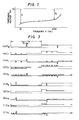
- the threshold voltage of the liquid crystal has a characteristic dependent on the frequency of applied voltage, and in case that the threshold voltage of the liquid crystal, a voltage at which ON-state of liquid crystal display elements begins to be visible, falls largely at lower frequencies, strong blurs occur in display according to particular display patterns when the driving method B is employed. For example, if the liquid crystal has a characteristic in which the threshold voltage V th drops at lower frequencies as is shown in Fig.
- the voltage V1 applied to the elements on A1, A2 and A3 areas with respect to their threshold voltages at their frequency is higher than the voltage V2 applied to the elements on B1 and B2 areas with respect to their threshold voltages at their frequency, and as a result, the degree of darkening of the elements on A1, A2 and A3 areas is higher than that of the non-selected elements on B1 and B2 areas and the phenomenon of blurs occurs around the display.
- the driving waveforms are shown in Figs. 3(a) to 3(j) which are applied to the display elements a1, a2, a3 and a4 shown in Fig. 2 by the driving method B.
- An object of the present invention is to provide a liquid crystal display device free from the blurs in display due to the lowering of the threshold voltage of the liquid crystal with low frequency.
- Another object of the present invention is to provide a liquid crystal device free from spurious signals in display due to the inversion of polarity of voltage applied to liquid crystal display elements.
- Fig. 1 shows the frequency dependence of the threshold voltage
- Fig. 2 is a diagram for illustrating the occurrence of blurs in display in the case of displaying the pattern of the alphabet E on the liquid crystal panel
- Figs.3(a) to 3(j) show timing charts of the operations in Fig. 2
- Fig. 4 is a graph showing variations in threshold voltage which are caused by the frequency
- Fig. 5 is a graph showing changes in luminance versus variations in threshold voltage
- Fig. 1 shows the frequency dependence of the threshold voltage
- Fig. 2 is a diagram for illustrating the occurrence of blurs in display in the case of displaying the pattern of the alphabet E on the liquid crystal panel
- Figs.3(a) to 3(j) show timing charts of the operations in Fig. 2
- Fig. 4 is a graph showing variations in threshold voltage which are caused by the frequency
- Fig. 5 is a graph showing changes in luminance versus variations in threshold voltage
- Fig. 1 shows the frequency dependence of the threshold voltage
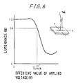
- FIG. 6 is a graph showing relationship between luminance and effective values of applied voltages, this graph being employed for a description of the threshold voltage;
- Figs 7(a) to 7(d) inclusive are charts for describing a method of increasing frequencies of the driving voltage with the help of a new control signal M'';
- Figs 8(a) to 8(e) inclusive are charts for explaining phasic relations between successsive frames and a ratio of the period of the control signal M' to the frame period;
- Figs. 9(a), 9(b) are charts for describing a phasic relation between the control signals M and M';
- Fig. 10 is a block diagram of liquid crystal modules which shows one example of a driving circuit designed for a liquid crystal display device according to the present invention;
- Figs. 10 is a block diagram of liquid crystal modules which shows one example of a driving circuit designed for a liquid crystal display device according to the present invention;
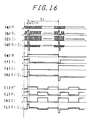
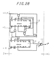
- FIG. 16(a) to 16(1) inclusive are charts of voltage waveforms which show comparison of driving frequencies by the driving methods A, B and the embodiment 1, respectively, when all the picture elements are to be on an ON-state; and Figs 17 to 28 inclusive are circuit diagrams each showing a still another embodiment of the liquid crystal driving circuit connected to that of Fig. 10.
- the frequency f D of a drive voltage appiled to the liquid crystal element is in the range of relation (1) where a frame frequency is f F and the number of scanning lines, namely the number of multiplexing is n. (1/2)f F ⁇ f D ⁇ (1/2)nf F (1)
- the drive frequency f D is, in this case, in the range of relation (2). 20 (Hz) ⁇ f D ⁇ 4500 (Hz) (2)
- Fig. 4 shows changes in threshold voltage Vth resulting from changes in drive frequency in terms of the percentage for the threshold voltage Vth (500 Hz) with drive frequency of 500 Hz
- Fig. 5 shows changes in luminance of liquid crystal display resulting from the change of threshold voltage Vth.
- the threshold voltage Vth is, as shown in Fig. 6, the effective value of the applied voltage in which the luminance observed in the direction inclined at an angle of 10° from the normal to the display surface amounts to 80%, which is designated as
- the threshold voltage Vth is lowered by 5% in the low frequency side as is apparent from Fig. 4 and thereby the luminance of liquid crystal display is changed by 10% or more with reference to Fig. 5, allowing generation of blur in display.
- the change of threshold voltage Vth must be suppressed to about 1.5% or less in view of keeping change of luminance at 10 % or less so that blur in display can not be detected, but the minimum value of drive frequency must be kept at 100 Hz or more in order to suppress changes in threshold voltage Vth to 1% or less considering some margin.
- the period for reversal of polarity of voltage applied to the liquid crystal element must be set larger than that of the driving method A but must be smaller than that of the driving method B.
- An example of drive signal waveform applied to the picture element a3 shown in Fig. 2 will be explained hereinafter. In Fig.
- the waveform (a) is a drive waveform applied to the picture element a3 during the drive by the driving method B
- the waveform (b) is a control signal M for reversing the polarity of voltage applied to liquid crystal layer during the driving method B, namely during the two frame period
- the waveform (c) is a new control signal M'' for increasing frequencies of drive waveform applied to the liquid crystal layer
- the waveform (d) is a drive waveform formed through inversion of polarity by the new control signal M''. Since the frequency of new control signal M'' is equal to triple that of control signal M for the driving method B, the frequency component of drive waveform applied to the picture element a3 is also tripled.
- the minimum frequency component, 20 Hz of the drive voltage in the driving method B can be set higher than the minimum driving frequency 100 Hz for suppressing the change in Vth to 1% or less by inverting the polarity of the drive voltage with the control signal having the period less than 1/5 of that of the control signal M whose period is double the frame period in the driving method B. Meanwhile, if the period of control signal is set excessively short, the driving method becomes similar to the method A and influences by the distortion of drive waveform on the effective value of drive voltage become large, and blurs in display are generated.
- FIG. 8 there are shown phasic relationships between a ratio of the frame period ⁇ F to the period ⁇ M' of the control signal M' and starting ends of successive frames.
- L is a positive integer
- the polarity of the control signal M' at the starting ends of the successive frames does not change.
- L -1/2 ⁇ ⁇ F / ⁇ M' ⁇ L (5) as shown in Figs 8(b), 8(c)
- the polarity of the control signal M'at the starting ends of the successive frames is inverted.
- ⁇ M' is set to a relation such as L -1 ⁇ ⁇ F / ⁇ M' ⁇ L - 1/2 , it is desirable to invert the control signal M' with the frame period ⁇ F .
- control signal M shows a phasic relation between the control signal M and the control signal M' in connection with the period ⁇ ALT , the control signal M' being generated by counting the clock signal and the control signal M being the signal for polarity reversal with the frame period ⁇ F .
- ⁇ ALT 2 . 2K . ⁇ F , Fig.
- Fig. 10 is a block diagram showing one example of the liquid crystal display device comprising a liquid crystal module and a control circuit for controlling this liquid crystal module.
- reference numeral 1 denotes a liquid crystal module comprising a liquid crystal display panel having a plurality of liquid crystal picture elements arranged on a matrix and driving circuits for the liquid crystal
- 2 denotes a control circuit (for example, Control Circuit Board for Graphic LCD display Modules CB 1026R available from Hitachi, Ltd.) for controlling the operation of the liquid crystal module 1.
- Numeral 3 denotes the liquid crystal display panel shown in Fig.
- the numeral 7 denotes a timing circuit for generating the latch signal CL1, data shift signal CL2 and the control signal M for AC driving as the timing signals to operate the liquid crystal module 1, and 8 a power supply for supplying the proper voltage to the power supply 6.
- Symbols D1 and D2 denote data terminals to which ON-OFF information for all picture elements on the signal electrodes Y1, Y2, Y3, ..., Y m are given serially as the inputs and FLM an input terminal to which the frame frequency signal is given as its input. Further explanation is made in "Liquid-Crystal Matrix Display", Image Pickup and Displays, IV Academic Press (1981).
- Figs. 11(a) to 11(d) are timing charts showing the output signals of the control circuit 2 shown in Fig. 10 by the driving method B.
- ON-OFF information signals for all picture elements on a certain scanning line are given to the data terminals D1 and D2 serially as inputs.
- the shift register in the signal electrode driving circuits 4a and 4b shifts the data according to the data shift signal CL2.
- a latch signal CL1 is outputted when the shift register is filled by the serial data and is latched by a latch circuit.
- the latch signal CL1 generates signals at every interval which equals the divided value of the frame period ⁇ F by n, which is the number of time multiplexed scanning lines and latches the data.
- the driving waveforms for the liquid crystal are converted into alternating waveforms by inverting the polarity within two frames and the complete alternating waveforms within the two frames can be obtained by the control signal M having a period which is twice the frame period ⁇ F .
- the lowest frequency component is low and this causes the blurs in display.
- the present invention is therefore characterized such that the new control signal M'' having a period shorther than that of the original control signal M based on the above-described driving method B is generated in place of the control signal M; and the liquid crystal driving waveforms are inverted in polarity for alternation by employing the new control signal M'', thereby driving the liquid crystal display device.
- the minimum driving frequency to be applied to the liquid crystal layer is 70 Hz.
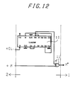
- a circuit is tangibly exemplified.
- a counter circuit 10 for outputting the new control signal M' by counting the latch signal CL1
- an Exclusive-OR circuit 11 for outputting a still newer control signal M'' by utilizing both the control signal M' and the original control signal M based on the driving method B which is outputted from the controller circuit 2.
- ten CL1 pulses are counted, and the CL1 is frequency-divided, thereby obtaining the new control signal M'.
- the still newer control signal M" is the output signal procured by a step wherein the counter output M' and the control signal M based on the driving method B that is outputted from the controller circuit 2 are exclusive-ORed.
- the still newer control signal M'' does not synchronizes with the frame signal FLM and hence the scanning line on which the inversion of polarity of the voltage to be applied to the liquid crystal is started moves per frame.
- an aspect of the movement is depicted by an arrowhead.
- the embodiment 2 involves the same step as that of the embodiment 1 wherein: the time-multiplexing number n is 64; the frame frequency f F is 70 Hz; the minimum driving frequency f Dmin exceeds 200 Hz; and ten CL1 pulses are counted thereby to generate the new control signal M'.
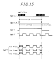
- the frame signal FLM is inputted to the reset signal terminals CLR1, CLR2 of the counter circuit 10, so that the counter circuit 10 synchronizes with the frame signal FLM every time that the same signal is inputted. Thereafter, the counter circuit 10 is reset so as to start counting the latch signal CL1, whereby the new control signal M' is outputted.
- Figs. 15(a) to 15(e) respectively show the timing of each of the signals employed in the embodiment 2.
- the still newer control signal M'' synchronizes with the frame frequency signal FLM and hence the scanning line on which the inversion of polarity of the voltage to be applied to the liquid crystal is started is fixed without moving per frame.
- Fig. 13 shows this situation with the help of an arrowhead.
- the minimum driving fequency can be set to a higher value than that in the conventional driving method B; and it is practicable to improve the display-unevenness that is caused by a decrease in threshold voltage Vth of the liquid crystal on the side of low frequencies.
- Figs 16(a) to 16(l) in combination show the respective driving waveforms of the voltage R1 on the scanning electrode and the signal voltage C1 in case of the all-dot-lighting of the liquid crystal panel shown in Fig. 2 by making a comparison between the driving method A, the driving method B and the driving method of the embodiment 1.
- Figs. 16(a) to 16(d) show the driving waveforms when the driving method A is employed;
- Figs. 16(e) to 16(h) show the driving waveforms when the driving method B is used;
- Figs. 16(i) to 16(1) show the driving waveforms when the driving method of the embodiment 1 is utilized.
- the driving frequency can be set to a value lower than that of the driving method A, while at the same time it can be set to a value higher than that of the driving method B. Hence, it is feasible to improve the above-described unevenness of display.
- the driving circuits depicted in Figs. 12 and 14 according to the present invention are simply constituted such that two pieces of CMOS LSI's are merely added to a conventional circuit. Such a constitution inevitably brings about no large increase in manufacturing costs.
- the configuration is the same as that of the conventional one, and compatibility of the system is favorable.
- FIG. 17 there is a shown a tangible circuit consisting of a binary counter 12 and an Ex-OR circuit 11.
- the still newer control signal M'' does not synchronize with the frame signal FLM. This is the same with the embodiment 1.
- the still newer control signal M'' that synchronizes with the frame signal FLM is similarly generated. This is the same with the embodiment 2.
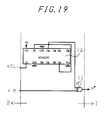
- Fig. 19 shows a concrete example of a circuit constituted by the binary counter 12 and the Ex-OR circuit 11. As in the case of the embodiment 1, the control signal M'' does not synchronize with the frame signal FLM.
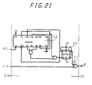
- Fig. 21 tangibly shows a circuit which comprises the binary counter 12, a flip-flop 13 and the Ex-OR circuit 11.
- the flip-flop 13 is herein employed to actualize the control signal M' having 50% duty.
- the control signal M'' does not synchronize with the frame signal FLM, which is the same with the embodiment 1.
- n 171 and the frame frequency f F is 70 Hz
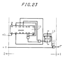
- Fig. 23 tangibly shows a circuit consisting of the binary counter 12, the flip-flop 13 and the Ex-OR circuit 11.
- the control signal M'' does not synchronize with the frame signal FLM. This is the same with the embodiment 1.
- the time-multiplexing n is 171
- the frame frequency f F is 70 Hz
- m is 56, which numerical values are the same as those of the embodiment 9.
- the control signal M'' that synchronizes with the frame signal FLM is generated, this being identical with the embodiment 2.
- Fig. 25 shows a tangible circuit which is constituted by the binary counter 12 and the Ex-OR circuit 11. The control signal M'' does not synchronize with the frame signal FLM. This is the same with the embodiment 1.
- the control signal M'' that synchronizes with the frame signal FLM is generated.
- the control signal M'' does not synchronize with the frame signal FLM, which is the same with the embodiment 1.
- the latch signal is frequency-divided when generating the signal M' in the above-described embodiments.
- the present invention is not, however, confined to this.
Landscapes
- Engineering & Computer Science (AREA)
- Chemical & Material Sciences (AREA)
- Crystallography & Structural Chemistry (AREA)
- Physics & Mathematics (AREA)
- Computer Hardware Design (AREA)
- General Physics & Mathematics (AREA)
- Theoretical Computer Science (AREA)
- Liquid Crystal Display Device Control (AREA)
- Liquid Crystal (AREA)
Claims (12)
- Flüssigkristallanzeigevorrichtung mit:- einem Flüssigkristallmodul (1) mit einem Flüssigkristallanzeigepaneel (3) mit mehreren Flüssigkristallanzeigeelementen, die matrixförmig angeordnet sind, und mit Treiberschaltungen (4a, 4b, 5) zum Anlegen von Treibersignalen an Signalelektroden (Y₁ ... Ym) bzw. an Rasterelektroden (X₁ ... X2n) des Flüssigkristallanzeigepaneels;- einer Steuerschaltung (2) zum Steuern des Betriebs des Flüssigkristallmoduls; und- einer Einrichtung zum Umkehren der Polarität einer Spannung, die an eine Flüssigkristallschicht anzulegen ist, die zwischen eine der Signalelektroden (Y₁ ... Ym) und eine der Rasterelektroden (X₁ ... X2n) eingebettet ist, durch Erzeugen eines Steuersignals,
dadurch gekennzeichnet, daß das Steuersignal M' eine Periode mτ aufweist, welches Signal die Polarität der an die Flüssigkristallschicht anzulegenden Spannung immer dann umkehrt, wenn ein Taktsignal einer Periode τ bis auf einen vorgegebenen Wert m/2 hochgezählt ist, wobei m eine positive gerade Zahl kleiner als 2n ist,- wobei dann, wenn nτ die Vollbildfrequenz und L eine willkürliche positive ganze Zahl ist,(1) m auf 2n/(2L-1) gesetzt wird, oder(2) m auf n/L gesetzt wird und das Steuersignal M' über eine Vollbildperiode im invertierten Zustand gehalten wird und in der nächsten Vollbildperiode im nicht invertierten Zustand gehalten wird, oder(3) m so eingestellt wird, daß es
 (4) m so eingestellt wird, daß es
 - und wobei weiterhin dann, wenn das kleinste gemeinsame Vielfache von 2n und m ein Wert H ist, die Werte von m so eingestellt werden, daß H/(2n) und H/m nicht beide gleichzeitig ungeradzahlige Zahlen sind.
 - Flüssigkristallanzeigevorrichtung nach Anspruch 1, bei der m und n die folgende ungleichung erfüllen: 2,0 ≦ n/m ≦ 6,0.
- Flüssigkristallanzeigevorrichtung nach Anspruch 2, bei der n kein ganzzahliges Vielfaches von m ist.
- Flüssigkristallanzeigevorrichtung nach Anspruch 1, bei der das Steuersignal M' nicht mit der Vollbildfrequenz synchronisiert.
- Flüssigkristallanzeigevorrichtung nach Anspruch 4, bei der sich Rasterelektroden (X₁ ... X2n), bei denen die Polarität der an die Flüssigkristallelemente zu legenden Spannung invertiert wird, um weniger als zehn Rasterelektroden von Vollbild zu Vollbild unterscheiden.
- Flüssigkristallanzeigevorrichtung nach Anspruch 1, bei der das Taktsignal ein Sperrsignal ist, um Informationsdaten für die Anzeige zwischenzuspeichern.
- Flüssigkristallanzeigevorrichtung mit:- einem Flüssigkristallmodul (1) mit einem Flüssigkristallanzeigepaneel (3), das in mehrere Blöcke (3a, 3b) unterteilt ist, mit mehreren in Matrixform angeordneten Flüssigkristallanzeigeelementen und mit Treiberschaltungen (4a, 4b, 5) zum Anlegen von Treibersignalen an Signalelektroden (Y₁ ... Ym) bzw. an Rasterelektroden (X₁ ... X2n) des Flüssigkristallanzeigepaneels;- einer Steuerschaltung (2) zum Steuern des Betriebs des Flüssigkristallmoduls; und- einer Einrichtung zum umkehren der Polarität einer Spannung, die an eine Flüssigkristallschicht anzulegen ist, die zwischen eine der Signalelektroden (Y₁ ... Ym) und eine der Rasterelektroden (X₁ ... X2n) eingebettet ist, durch Erzeugen eines Steuersignals,
dadurch gekennzeichnet, daß das Steuersignal M' eine Periode mτ aufweist, welches Signal die Polarität der an die Flüssigkristallschicht anzulegenden Spannung immer dann umkehrt, wenn ein Taktsignal einer Periode τ bis auf einen vorgegebenen Wert m/2 hochgezählt ist, wobei m eine positive gerade Zahl kleiner als 2n ist,- wobei dann, wenn die nτ Vollbildfrequenz und L eine willkürliche positive ganze Zahl ist,(1) m auf 2n/(2L-1) gesetzt wird, oder(2) m auf n/L gesetzt wird und das Steuersignal M' über eine Vollbildperiode im invertierten Zustand gehalten wird und in der nächsten Vollbildperiode im nicht invertierten Zustand gehalten wird, oder(3) m so eingestellt wird, daß es
 (4) m so eingestellt wird, daß es
 - und wobei weiterhin dann, wenn das kleinste gemeinsame Vielfache von 2n und m ein Wert H ist, die Werte von m so eingestellt werden, daß H/(2n) und H/m nicht beide gleichzeitig ungeradzahlige Zahlen sind.
 - Flüssigkristallanzeigevorrichtung nach Anspruch 7, bei der m und n die folgende ungleichung erfüllen: 2,0 ≦ n/m ≦ 6,0.
- Flüssigkristallanzeigevorrichtung nach Anspruch 8, bei der n kein ganzzahliges Vielfaches von m ist.
- Flüssigkristallanzeigevorrichtung nach Anspruch 7, bei der das Steuersignal M' nicht mit der Vollbildfrequenz synchronisiert.
- Flüssigkristallanzeigevorrichtung nach Anspruch 10, bei der sich Rasterelektroden (X₁ ... X2n), bei denen die Polarität der an die Flüssigkristallelemente zu legenden Spannung invertiert wird, um weniger als zehn Rasterelektroden von Vollbild zu Vollbild unterscheiden.
- Flüssigkristallanzeigevorrichtung nach Anspruch 7, bei der das Taktsignal ein Sperrsignal ist, um Informationsdaten für die Anzeige zwischenzuspeichern.
Applications Claiming Priority (2)
| Application Number | Priority Date | Filing Date | Title |
|---|---|---|---|
| JP60169807A JPS6231825A (ja) | 1985-08-02 | 1985-08-02 | 液晶表示装置用駆動回路 |
| JP169807/85 | 1985-08-02 |
Publications (3)
| Publication Number | Publication Date |
|---|---|
| EP0211599A2 EP0211599A2 (de) | 1987-02-25 |
| EP0211599A3 EP0211599A3 (en) | 1989-02-22 |
| EP0211599B1 true EP0211599B1 (de) | 1993-01-07 |
Family
ID=15893258
Family Applications (1)
| Application Number | Title | Priority Date | Filing Date |
|---|---|---|---|
| EP86305822A Expired - Lifetime EP0211599B1 (de) | 1985-08-02 | 1986-07-29 | Flüssigkristallanzeigegerät |
Country Status (4)
| Country | Link |
|---|---|
| US (1) | US4746197A (de) |
| EP (1) | EP0211599B1 (de) |
| JP (1) | JPS6231825A (de) |
| DE (1) | DE3687435T2 (de) |
Families Citing this family (17)
| Publication number | Priority date | Publication date | Assignee | Title |
|---|---|---|---|---|
| EP0287055B1 (de) * | 1987-04-15 | 1993-09-29 | Sharp Kabushiki Kaisha | Flüssigkristallanzeigegerät |
| US5179371A (en) * | 1987-08-13 | 1993-01-12 | Seiko Epson Corporation | Liquid crystal display device for reducing unevenness of display |
| US5175535A (en) * | 1987-08-13 | 1992-12-29 | Seiko Epson Corporation | Circuit for driving a liquid crystal display device |
| US5202676A (en) * | 1988-08-15 | 1993-04-13 | Seiko Epson Corporation | Circuit for driving a liquid crystal display device and method for driving thereof |
| JP2906057B2 (ja) * | 1987-08-13 | 1999-06-14 | セイコーエプソン株式会社 | 液晶表示装置 |
| US5214417A (en) * | 1987-08-13 | 1993-05-25 | Seiko Epson Corporation | Liquid crystal display device |
| US5184118A (en) * | 1987-08-13 | 1993-02-02 | Seiko Epson Corporation | Liquid crystal display apparatus and method of driving same |
| US5642128A (en) * | 1987-10-02 | 1997-06-24 | Canon Kabushiki Kaisha | Display control device |
| JPH01134497A (ja) | 1987-11-20 | 1989-05-26 | Semiconductor Energy Lab Co Ltd | 液晶表示装置の電源回路 |
| DE69027136T2 (de) * | 1989-02-10 | 1996-10-24 | Sharp Kk | Flüssigkristallanzeigeeinheit und Steuerverfahren dafür |
| EP0384229B1 (de) * | 1989-02-23 | 1995-05-10 | Seiko Epson Corporation | Flüssigkristallanzeigeeinheit |
| US5473338A (en) * | 1993-06-16 | 1995-12-05 | In Focus Systems, Inc. | Addressing method and system having minimal crosstalk effects |
| JP3531164B2 (ja) * | 1992-05-14 | 2004-05-24 | セイコーエプソン株式会社 | 液晶表示装置及びそれを用いた電子機器 |
| US5861869A (en) * | 1992-05-14 | 1999-01-19 | In Focus Systems, Inc. | Gray level addressing for LCDs |
| JP2924623B2 (ja) * | 1994-01-04 | 1999-07-26 | 富士ゼロックス株式会社 | 光書き込み型液晶表示記録装置 |
| KR100224738B1 (ko) * | 1995-12-28 | 1999-10-15 | 손욱 | 단순 행렬형 엘시디의 구동 방법 |
| JP3417514B2 (ja) * | 1996-04-09 | 2003-06-16 | 株式会社日立製作所 | 液晶表示装置 |
Family Cites Families (15)
| Publication number | Priority date | Publication date | Assignee | Title |
|---|---|---|---|---|
| JPS5757718B2 (de) * | 1973-10-19 | 1982-12-06 | Hitachi Ltd | |
| JPS5416894B2 (de) * | 1974-03-01 | 1979-06-26 | ||
| JPS54143093A (en) * | 1978-04-28 | 1979-11-07 | Citizen Watch Co Ltd | Liquid crystal display unit |
| JPS57198491A (en) * | 1981-06-01 | 1982-12-06 | Seiko Instr & Electronics | Image display unit |
| US4404555A (en) * | 1981-06-09 | 1983-09-13 | Northern Telecom Limited | Addressing scheme for switch controlled liquid crystal displays |
| US4525710A (en) * | 1982-02-16 | 1985-06-25 | Seiko Instruments & Electronics Ltd. | Picture display device |
| JPS59113420A (ja) * | 1982-12-21 | 1984-06-30 | Citizen Watch Co Ltd | マトリクス表示装置の駆動方法 |
| JPS6019196A (ja) * | 1983-07-13 | 1985-01-31 | 三菱電機株式会社 | 液晶表示装置の駆動方法及びその装置 |
| JPS6045294A (ja) * | 1983-08-23 | 1985-03-11 | セイコーエプソン株式会社 | 液晶表示パネルの駆動装置 |
| US4651148A (en) * | 1983-09-08 | 1987-03-17 | Sharp Kabushiki Kaisha | Liquid crystal display driving with switching transistors |
| JPS60140297A (ja) * | 1983-12-28 | 1985-07-25 | 松下電器産業株式会社 | ドツトマトリクス液晶表示装置駆動回路 |
| JPH0762788B2 (ja) * | 1984-05-23 | 1995-07-05 | シチズン時計株式会社 | 液晶マトリクス表示パネルの駆動方式 |
| JPS6150119A (ja) * | 1984-08-20 | 1986-03-12 | Hitachi Ltd | 液晶表示装置用駆動回路 |
| US4691200A (en) * | 1984-10-01 | 1987-09-01 | Xerox Corporation | Matrix display with a fast cursor |
| JPH0782167B2 (ja) * | 1984-10-23 | 1995-09-06 | セイコー電子工業株式会社 | 液晶表示装置 |
-
1985
- 1985-08-02 JP JP60169807A patent/JPS6231825A/ja active Pending
-
1986
- 1986-07-24 US US06/888,864 patent/US4746197A/en not_active Expired - Fee Related
- 1986-07-29 EP EP86305822A patent/EP0211599B1/de not_active Expired - Lifetime
- 1986-07-29 DE DE8686305822T patent/DE3687435T2/de not_active Expired - Fee Related
Also Published As
| Publication number | Publication date |
|---|---|
| EP0211599A3 (en) | 1989-02-22 |
| DE3687435T2 (de) | 1993-05-06 |
| EP0211599A2 (de) | 1987-02-25 |
| US4746197A (en) | 1988-05-24 |
| DE3687435D1 (de) | 1993-02-18 |
| JPS6231825A (ja) | 1987-02-10 |
Similar Documents
| Publication | Publication Date | Title |
|---|---|---|
| US4746197A (en) | Driving circuit for liquid crystal display device | |
| US4702560A (en) | Liquid crystal display device | |
| US4926168A (en) | Liquid crystal display device having a randomly determined polarity reversal frequency | |
| US7095397B2 (en) | Drive method, a drive circuit and a display device for liquid crystal cells | |
| US7362294B2 (en) | Low power LCD with gray shade driving scheme | |
| JPWO1993018501A1 (ja) | 液晶素子等の駆動方法と駆動回路および表示装置 | |
| JPH0473845B2 (de) | ||
| JPH0822267A (ja) | 液晶駆動回路と液晶表示装置 | |
| EP0704087B1 (de) | Verfahren zur steuerung eines bildanzeigegeräts | |
| US5754152A (en) | Drive method and drive unit for a liquid crystal display device reducing variation of applied voltage dependent upon display patterns | |
| US4701025A (en) | Liquid crystal display device with driving method to eliminate blur due to frequency dependence | |
| US5541619A (en) | Display apparatus and method of driving display panel | |
| US5216417A (en) | Multi-tone level displaying method by bi-level display devices and multi-tone level displaying unit | |
| US5801671A (en) | Liquid crystal driving device | |
| GB1592795A (en) | Data display screen systems utilising a bistable voltage-controlled medium | |
| US7619601B2 (en) | Display device and display method | |
| JP3015014B2 (ja) | 液晶表示装置 | |
| EP0293235B1 (de) | Anzeigegerät und Ansteuersystem dafür | |
| JP2942229B2 (ja) | 液晶表示装置 | |
| JP3054149B2 (ja) | 液晶表示装置 | |
| JP3146448B2 (ja) | 液晶表示装置 | |
| JP3270086B2 (ja) | 液晶表示装置 | |
| JPH05173508A (ja) | 液晶表示装置の駆動方法 | |
| JP3128551B2 (ja) | 液晶表示装置 | |
| JP3618141B2 (ja) | 画像表示装置の駆動法 |
Legal Events
| Date | Code | Title | Description |
|---|---|---|---|
| PUAI | Public reference made under article 153(3) epc to a published international application that has entered the european phase |
Free format text: ORIGINAL CODE: 0009012 |
|
| AK | Designated contracting states |
Kind code of ref document: A2 Designated state(s): DE FR GB |
|
| RIN1 | Information on inventor provided before grant (corrected) |
Inventor name: KINUGAWA, KIYOSHIGE Inventor name: MATSUDO, TOSHIMITSU Inventor name: SAKUMA, TOSHIYUKI Inventor name: ENDO, SHYUSUKE |
|
| PUAL | Search report despatched |
Free format text: ORIGINAL CODE: 0009013 |
|
| AK | Designated contracting states |
Kind code of ref document: A3 Designated state(s): DE FR GB |
|
| 17P | Request for examination filed |
Effective date: 19890706 |
|
| 17Q | First examination report despatched |
Effective date: 19910712 |
|
| GRAA | (expected) grant |
Free format text: ORIGINAL CODE: 0009210 |
|
| AK | Designated contracting states |
Kind code of ref document: B1 Designated state(s): DE FR GB |
|
| REF | Corresponds to: |
Ref document number: 3687435 Country of ref document: DE Date of ref document: 19930218 |
|
| ET | Fr: translation filed | ||
| PLBE | No opposition filed within time limit |
Free format text: ORIGINAL CODE: 0009261 |
|
| STAA | Information on the status of an ep patent application or granted ep patent |
Free format text: STATUS: NO OPPOSITION FILED WITHIN TIME LIMIT |
|
| 26N | No opposition filed | ||
| PGFP | Annual fee paid to national office [announced via postgrant information from national office to epo] |
Ref country code: FR Payment date: 19970709 Year of fee payment: 12 |
|
| PGFP | Annual fee paid to national office [announced via postgrant information from national office to epo] |
Ref country code: GB Payment date: 19970721 Year of fee payment: 12 |
|
| PGFP | Annual fee paid to national office [announced via postgrant information from national office to epo] |
Ref country code: DE Payment date: 19970801 Year of fee payment: 12 |
|
| PG25 | Lapsed in a contracting state [announced via postgrant information from national office to epo] |
Ref country code: GB Free format text: LAPSE BECAUSE OF NON-PAYMENT OF DUE FEES Effective date: 19980729 |
|
| GBPC | Gb: european patent ceased through non-payment of renewal fee |
Effective date: 19980729 |
|
| PG25 | Lapsed in a contracting state [announced via postgrant information from national office to epo] |
Ref country code: FR Free format text: LAPSE BECAUSE OF NON-PAYMENT OF DUE FEES Effective date: 19990331 |
|
| PG25 | Lapsed in a contracting state [announced via postgrant information from national office to epo] |
Ref country code: DE Free format text: LAPSE BECAUSE OF NON-PAYMENT OF DUE FEES Effective date: 19990501 |
|
| REG | Reference to a national code |
Ref country code: FR Ref legal event code: ST |