EP0212905A2 - Appareil pour décoder des codes d'image - Google Patents
Appareil pour décoder des codes d'image Download PDFInfo
- Publication number
- EP0212905A2 EP0212905A2 EP86306006A EP86306006A EP0212905A2 EP 0212905 A2 EP0212905 A2 EP 0212905A2 EP 86306006 A EP86306006 A EP 86306006A EP 86306006 A EP86306006 A EP 86306006A EP 0212905 A2 EP0212905 A2 EP 0212905A2
- Authority
- EP
- European Patent Office
- Prior art keywords
- image
- code
- codes
- decoding
- discriminating
- Prior art date
- Legal status (The legal status is an assumption and is not a legal conclusion. Google has not performed a legal analysis and makes no representation as to the accuracy of the status listed.)
- Granted
Links
- 238000012544 monitoring process Methods 0.000 claims abstract 3
- 238000007599 discharging Methods 0.000 claims description 9
- 230000000694 effects Effects 0.000 claims description 4
- 235000014676 Phragmites communis Nutrition 0.000 abstract description 4
- 230000015654 memory Effects 0.000 description 35
- 230000006870 function Effects 0.000 description 16
- 238000001514 detection method Methods 0.000 description 13
- 238000010586 diagram Methods 0.000 description 13
- 238000000034 method Methods 0.000 description 13
- 230000008569 process Effects 0.000 description 13
- 230000004044 response Effects 0.000 description 8
- 238000006073 displacement reaction Methods 0.000 description 7
- 230000006835 compression Effects 0.000 description 4
- 238000007906 compression Methods 0.000 description 4
- 230000001172 regenerating effect Effects 0.000 description 4
- 230000000977 initiatory effect Effects 0.000 description 3
- 230000001360 synchronised effect Effects 0.000 description 2
- 230000008859 change Effects 0.000 description 1
- 238000004891 communication Methods 0.000 description 1
- 230000001276 controlling effect Effects 0.000 description 1
- 238000005259 measurement Methods 0.000 description 1
- 230000003287 optical effect Effects 0.000 description 1
- 238000005192 partition Methods 0.000 description 1
- 238000002360 preparation method Methods 0.000 description 1
- 238000001454 recorded image Methods 0.000 description 1
- 230000008929 regeneration Effects 0.000 description 1
- 238000011069 regeneration method Methods 0.000 description 1
- 230000001105 regulatory effect Effects 0.000 description 1
Images






Classifications
-
- H—ELECTRICITY
- H04—ELECTRIC COMMUNICATION TECHNIQUE
- H04N—PICTORIAL COMMUNICATION, e.g. TELEVISION
- H04N1/00—Scanning, transmission or reproduction of documents or the like, e.g. facsimile transmission; Details thereof
- H04N1/41—Bandwidth or redundancy reduction
- H04N1/411—Bandwidth or redundancy reduction for the transmission or storage or reproduction of two-tone pictures, e.g. black and white pictures
- H04N1/413—Systems or arrangements allowing the picture to be reproduced without loss or modification of picture-information
- H04N1/417—Systems or arrangements allowing the picture to be reproduced without loss or modification of picture-information using predictive or differential encoding
- H04N1/4175—Systems or arrangements allowing the picture to be reproduced without loss or modification of picture-information using predictive or differential encoding involving the encoding of tone transitions with respect to tone transitions in a reference line
-
- H—ELECTRICITY
- H03—ELECTRONIC CIRCUITRY
- H03M—CODING; DECODING; CODE CONVERSION IN GENERAL
- H03M7/00—Conversion of a code where information is represented by a given sequence or number of digits to a code where the same, similar or subset of information is represented by a different sequence or number of digits
- H03M7/30—Compression; Expansion; Suppression of unnecessary data, e.g. redundancy reduction
- H03M7/46—Conversion to or from run-length codes, i.e. by representing the number of consecutive digits, or groups of digits, of the same kind by a code word and a digit indicative of that kind
Definitions
- the present invention relates to a decoding apparatus for image codes, and in particular a decoding apparatus for image codes obtained by two-dimensional encoding such as modified Reed (MR) encoding or modified modified Reed (MMR) encoding.
- MR modified Reed
- MMR modified modified Reed
- image transmitting apparatus such as facsimile or image files utilizing optical disks or magnetic disks
- high-speed and efficient transmitting or accumulating operation is achieved through compression of image data.
- MR and MMR encoding processes are generally known as disclosed in the Notification Nos. 1013, 1981 of Japanese Ministry of Postal Service for two-dimensional encoding process and in the Notification Nos. 197, 1985 of Japanese Ministry of Postal Service for high-efficiency two-dimensional encoding process.
- the codes represent the relationship between the image signals of a line to be encoded and the image signals of a preceding line. Consequently the decoding of such two-dimensionally encoded image codes necessitates a complex process for discriminating the relationship between the input image codes and the already decoded image signals of a preceding line, and such process has been conducted by a software for example of a microcomputer. Thus the discrimination of an image code sometimes requires several steps. Therefore high-speed decoding operation is sometimes not possible since a succeeding image code may not be decoded immediately.
- the length of obtained image codes is not necessarily uniform. Consequently, after a decoding operation, in order to prepare a succeeding code ready for decoding, the succeeding code is taken in according to the length of already decoded code. However, if the decoding time is short in comparison with the code length, the decoding operation may be interrupted since the succeeding code may not yet be ready for decoding when the decoding operation should be initiated.
- the relationship between the image signals of a line to be encoded and those of a preceding line is represented by codes of plural modes, and, in the horizontal mode among such plural modes, there are required an identification code indicating the horizontal mode and plural codes indicating the run length.
- the horizontal mode is discriminated by the identification code, and the run length is identified in a next step.
- the decoding operation may be interrupted in such operation, since a succeeding code cannot be processed immediately if the run length is short.
- the encoded image signals are decoded as explained above, and the decoded image signals are then supplied to a process unit such as a printer.
- a process unit such as a printer.
- an object of the present invention is to enable high-speed decoding of image codes.
- Another object of the present invention is to enable decoding of two-dimensionally encoded image codes, such as obtained by MR or MMR encoding, without interruption and without delay in supply to an output unit.
- Still another object of the present invention is to adapt a decoding apparatus to various process units.
- Still another object of the present invention is to enable high-speed decoding operation through high-speed discrimination of the relationship between input image codes and a reference image line by releasing image information of the reference line by a predetermined number of pixels at a time in parallel manner and forming image signals from the result of discrimination of image codes and said image information.
- Still another object of the present invention is to enable high-speed decoding operation without interruption in decoding the image codes of different code lengths, by varying the decoding operation for a succeeding code according to a preceding code discriminated in the decoding operation.
- Still another object of the present invention is to enable high-speed decoding operation without delay in the decoding of two-dimensionally encoded image codes such as obtained by MR or MMR encoding, by simultaneously discriminating an identification code indicating the encoding mode and a succeeding image code.
- Still another object of the present invention is to enable high-speed decoding operation in the decoding of two-dimensionally encoded image codes such as obtained by MR or MMR encoding, by immediately decoding an image code without the release of an identification code indicating the encoding mode.
- Still another object of the present invention is to enable accurate decoding operaiton, by starting the decoding operation after fetching the image signals of a predetermined number of pixels in the reference line necessary for the decoding of image codes.
- Still another object of the present invention is to enable the common use of a decoding apparatus for various output devices, by effecting the decoding operation in synchronization with clock signals thereby enabling to match the decoding operation with the function of such output device, for example a printer.
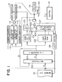
- Fig. 1 showing a block diagram of a decoding circuit embodying the present invention.
- the decoding of MMR encoded image codes but it is also applicable to other two-dimensional encoding such as MR encoding.
- the image line to be encoded is called a coding line
- an image line immediately preceding said coding line is called a reference line.
- the coding line is encoded according to the positional relationship of changing points in said coding line and those in said reference line.
- a memory circuit 101 stores image codes to be decoded (hereinafter simply called codes).
- Said memory circuit 101 stores serial codes, for example received from a communication line as shown in Fig. 2A , after division into parallel data of 16 bits as shown in Fig. 2B , regardless of the partition of the codes.
- Said memory circuit 101 can be composed of random access memories (RAM) or latch circuits.
- the memory circuit 101 is capable of renewing parallel output data BO - B15, in response to an external request signal 201.
- a multiplexer 102 and a register C 103 constitute a bit shifter.
- a code of 16 bits read in parallel manner from the memory circuit 101 is guided through the multiplexer 102 and stored in the register C 103.
- a shift control circuit 108 controls the input and output of the multiplexer 102 to displace the code data in one direction in the register C 103, by a number of bits designated by said shift control circuit 108.
- a code detection logic circuit 104 and a code table ROM 106 constitute a circuit for receiving a code in a predetermined position in the register C 103 to discriminate the content of said code. More specifically, the ROM 106 is provided with a table, storing run lengths and code lengths corresponding to the input codes in the horizontal (H) mode, and is adapted to release corresponding data by making access to said table. The run length data indicating the run length, released from the ROM 106, are supplied to a run length counting circuit 107.
- Said run length counting circuit 107 upon making a count equal to the number from the ROM 107, supplies a count end pulse to an image regenerating circuit 110 etc.
- the code length data obtained as a part of the output from the ROM 106, are supplied to the shift control circuit 108, which thus controls the multiplexer 102 to shift the code data in the register C 103 by the number of bits of code length of thus discriminated code. In this manner a discriminated code is discharged from the register C 103, and a succeeding code is moved to a predetermined position in the register C 103 for enabling discrimination by the ROM 106 etc.
- the shift control circuit 108 sums up the amount of movement of the code instructed to the multiplexer 102, and supplies a new 16-bit code in parallel manner from the memory circuit 101 to the register C 103 through the multiplexer 102 each time said sum reaches a value corresponding to a shift of 16 bits.
- the code detecting logic circuit 104 effects a detecting function when a particular code is present in the register C 103 as will be explained later, and supplies the result of detection to a PV reference circuit 105.
- Code length data of the particular code detected by the code detecting logic circuit 104 are also supplied to the shift control circuit 108, which performs a function as explained before.
- Line buffer memories A 112 and B 113 are respectively capable of storing image of an image line and are composed for example of random access memories.
- Address counters A 111 and B 117 are provided for designating read or write addresses of the buffer memories A 112 and B 113, which constitute a double buffer structure in which either memory is in the write mode while the other is in the read mode.
- Said buffer memories A 112 and B 113 are provided for storing image data of the reference line, required for decoding two-dimensionally encoded image codes obtained for example MR or MMR encoding.
- a control circuit 118 is provided to generate control signals for controlling the function of various circuit blocks shown in Fig. 1, which function in mutual synchronization, utilizing the clock signals generated by the control circuit 118 as common timing signals.
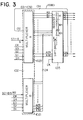
- the multiplexer 102 and the register C 103 constitute a bit shifter as explained before, of a structure as shown in Fig. 3.
- first one word or 16 bits (BO - B15) of the code data stored in the memory circuit 101 as shown in Fig. 2(B) are moved, through a multiplexer B 1021 shown in Fig. 3, to the shift register C 103, of which output is supplied through a multiplexer A 1022, again to the register C 103.
- This operation is interrupted when the first bit of said code appears as the output CO of the register C 103. In this state the preparation for decoding operation is completed.
- the above-explained displacement of code data is controlled by signals El - E4, CR, STl - ST8 from the shift control circuit 108 shown in Fig. 1 and signals SO - S3 from the code detecting logic circuit 104.
- the bit shifter composed of the multiplexer 102 and the register C 103 has two shift functions, i.e., a serial shift of one bit at a time and a jump shift of one to nine bits at a time.
- the register C 103 is composed of a 31-bit parallel-in-parallel-out register, with one- directional shift as indicated by an arrow in Fig. 3.
- the code shown in the register C 103 is an example of the code transferred from the memory circuit 101 to a decoding ready position in said register C 103 by the displacing function of the bit shifter.
- Fig. 4 shows the structure of the code table ROM 106 shown in Fig. 1, wherein provided are ordinary read-only memories (ROM) 401, 402, each having 13-bit address input ports AO - A12, a 1-bit chip enable input port CE and 12-bit data output ports 01 - 012.
- ROM read-only memories
- a signal to the chip enable input port CE selects either the ROM A 401 constituting a white code table or the ROM B 402 constituting a black code table.
- the output signal C3 of the register C 103 shown in Fig. 3 is supplied to the most significant bit (MSB) A12 of the address input ports of the ROM A 401, and the output signals C4 - C15 of said register C 103 are supplied, in parallel manner, to the succeeding address input ports All - A0. Also the input port CE of the ROM A 401 receives a black/white color signal B/W of the code.
- the output signal C3 is the most significant bit of various codes other than an H-mode code "001" representing the H-mode.
- run length data of said code (RL5 - RLO), code length data (CL4 - CLO) and a signal M/T indicating whether said code is a makeup code or a terminating code.
- the run length code is discriminated from the output signals C3 - C15 of the register C 103.
- Example shown in Fig. 4 indicates output signals in case the ROM 106 receives a code for a white run of 18 bits "0100111".
- the run length "18" is represented as a binary compliment of 2, i.e., "101110". Though the run length is usually represented by 12 bits, lower 6 bits alone are released for a terminating code since the upper 6 bits are all "1", and upper 6 bits alone are released for a makeup code since the lower 6 bits are all "0".
- output signals CL4 - CLO are "00111” indicating the code length "7" of the white 18-bit run code.
- the output singal M/T is "0" indicating that the entered code is a terminating code.
- the content of the ROM A 401 is so alotted for each entered code that addresses receiving no entry due to a short length of code have a value "DON'T CARE", and the employed codes are mutually so designed as not to cause confusion by the presence of such "DON'T CARE" bits.
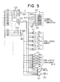
- Fig. 5 shows an example of the structure of the code detecting logic circuit 104 shown in Fig. 1.
- Said circuit discriminates the codes shown in Tables 1 and 2 by means of NAND gates 510, OR gates 511 and inverters 512, and releases a code detection signal, code length data (SO - S4) of the detected code, and run length data (RLO - RL5) thereof.
- a JCD signal 501 indicates the detection of any of the codes shown in Tables 1 and 2. Since the data from the register C 103 shown in Fig. 3 are supplied both to the ROM shown in Fig. 4 and the logic circuit shown in Fig. 5, the decoded data may be obtained from both. Thus, in case the logic circuit shown in Fig. 5 detects a code, the JCD signal cancels the output of the ROM shown in Fig. 4, thus giving priority to the decoding output of the logic'circuit shown in Fig. 5.
- Fig. 5 illustrates detection of P-code "0001", VL(l)-code "010” and W4-code "1011” among those listed in Tables 1 and 2, but other codes can be detected similarly.
- Tables 1 and 2 show codes for which a succeeding code cannot be brought to the decoding position in time by bit-by-bit shifts in the register C 103 of a number of clocks required for forming image data from the code, for example those codes for which the code length is equal to or longer than the run length represented by said codes.
- the predetermined detecting position is defined by a state in which the MSB bit of said code is positioned at CO of the register C 103 shown in Fig. 3.
- said predetermined position is defined by a state in which the MSB bit of said code is positioned at C3 of said register C 103.
- the codes shown in Tables 1 and 2 are collectively called jump codes. Natually other additional codes may be included in such jump codes.
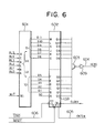
- Fig. 6 shows the detailed structure of the run length count circuit 107 shown in Fig. 1.
- a demultiplexer 601 receives the run length data RL5 - RLO, in the form of a compliment of 2, from the code table ROM 106 shown in Fig. 4, and supplies load (prese) data to a run length counter 602.
- the run length data RL5 - RLO supplied form the code table ROM contain only 6 bits as explained before, and the demultiplexer 601 replenishes lower or upper six bits "1" according to whether the entered code is a makeup code or a terminating code.
- An input signal M/T to the demultiplexer 601 functions as a select signal for determining whether the entered run length data RL5 - RLO are released to output ports Yl or Y2.
- the run length counter 602 is composed of a 12-bit binary counter.
- the run length counter 602 After presetting of an initial value (loading of the output of the multiplexer 601) by a LOAD signal 606 and after being enabled by a CNTEN signal 605, the run length counter 602 counts up the entered clock signals.
- output signals QO - Qll of the counter reach a state of all "1" or (-1)
- a gate 603 releases a zero output whereby an inverter 607 releases a count end pulse HCRO 604 to terminate the counting operation.
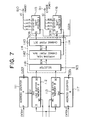
- FIG. 7 for explaining the processing of the image signals read from the line buffer memories A 112 and B 113, under the control of the address counters A 111 and B 117 shown in Fig. 1.
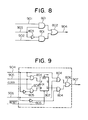
- an image converting circuit 114 is composed of a selector 1141, a hypothetical changing point generating circuit 1142 and a changing point detection circuit 1143. Details of the selector circuit 1141 are shown in Fig. 8, wherein provided are AND gates 801, an OR gate 802 and an inverter 803. Data 901 read from the line buffer memory A 112 and data 902 read from the line buffer memory B 113 are alternately selected as reference image signals 904 for each line by means of a switching signal 903.
- Fig. 9 shows the details of the hypothetical changing point generating circuit 1142, provided with AND gates 804, inverters 805, an OR gate 806 and a flip-flop 907.
- the flip-flop 907 fetches the color of the last pixel of the image signals 904 of each reference line. Then, at the end of a horizontal synchronization signal 906, indicating the effective period of each line, the output Q of the flip-flop 807 is so selected that a succeeding pixel (hypothetical pixel) always assumes a color opposite to that of the pixel latched in the flip-flop 807, thus always forming a changing point.
- Fig. 10 shows the changing point detection circuit 1143, composed of a flip-flop 1001, an exclusive OR gate 1002, and an inverter 1003.
- the output signal 907 of the hypothetical changing point generating circuit 1142 is supplied to the flip-flop 1001 and the exclusive OR gate 1002, and the output Q of said flip-flop 1001 is also supplied to the exclusive OR gate 1002 to detect a color change in neighboring pixels thus releasing a detection signal 909.
- Fig. 11 is a timing chart showing the function of the circuits 1142, 1143 shown in Figs. 9 and 10.
- a 4-bit shift register A 115 shown in Fig. 1 corresponds to that 115 shown in Fig. 7.
- Image data 908 of the reference line supplied from the changing point detection circuit 1143 to a terminal SI are shifted in succession by the clock signals, in the register A 115 in a direction from Q1 to Q4.
- the contents of said 4-bit register A 115 are always released as parallel signals 910 form terminals Cl - C4.
- the shift register A 115 always provides, in parallel manner, color information of four consecutive pixels of the reference line.
- a 4-bit shift register A 116 shown in Fig. 1 corresponds to the register 116 shown in Fig. 7.
- image changing point signal 909 of the reference line supplied from the changing point detection circuit 1143 to a terminal SI is shifted in succession in the shift register B 116, in a direction from Ql to Q4 in response to clock signals.
- the content of said shift register is released as parallel signals 911 composed of B1 - B4.
- the shift register B 116 always releases, in parallel manner, information indicating the presence and position of changing points in consecutive four pixels in the reference line.
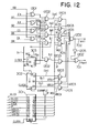
- Fig. 12 shows the details of the PV reference circuit 105 shown in Fig. 1, wherein provided are exclusive OR gates 1201, 703, AND gates 1202, 704, NAND gates 1203, 705, an inverter 1205, and an 8-bit latch circuit 301.
- the code detecting logic circuit 104 shown in Fig. 5 releases data in which a bit corresponding to the detected code alone is "1" and other bits are all "0", and the latch 301 receives and stores said code.
- the stored data are used as reference in the decoding of P- or V-mode.
- singals B1 - B4 correspond to the signal 911 from the register B 116 shown in Fig.
- signals Cl - C4 correspond to the signal 910 from the register A 115 shown in Fig. 7.
- signals a signal a 0 in Fig. 12 corresponds to the symbol a0 in two-dimensional encoding and indicates the color of starting pixel at each point of decoding. In the following other symbols will be represented likewise.
- the execlusive OR gate 703 and AND gate 704 detect that a symbol b 1 is positioned at C4 in the shift register A115 in Fig. 7.
- the flip-flop 303 in Fig. 12 is set by the output signal of the AND gate 704, thus memorizing that the symbol b 1 has been detected in the above-mentioned position.
- a 3-bit shift register 302 receives, through a terminal SI thereof, the symbol b 1 detected by said AND gate 704, and stores said symbol for succeeding three clock signals while it is transferred from Ql to Q3.
- the signal VHiT is released when the output Q2 of the shift register 302 becomes “1” if a signal VR(2) is latched in the latch 301, or when the output of the AND gate 1202 becomes “1” if a signal VL(2) is latched in the latch 301.
- the signal PVHiT indicates the completion of decoding of a V- or P-mode code, and the mode of a succeeding code is discriminated in response to said signal PVHiT.
- Fig. 13 shows the details of the shift control circuit 108 shown in Fig. 1, wherein provided are a 4-bit binary full-adder 1301 and a 4-bit latch 1302 which constitute a 4-bit binary accumulator.
- Input signals SO - S3 to the full-adder 1301 are obtained from the code detecting logic circuit 104 in Fig. 1 or from the code table ROM 106, and said signals indicate the amount of displacement of a code per clock in the register C 103.
- the amount of displacement obtained from the ROM 106 is always "1".
- the accumulator composed of the full-adder 1301 and the latch 1302 accumulates the number of empty bits in the register C, generated by the displacement of data therein.
- a new code of 16 bits read in parallel manner from the memory circuit 101 are added to the positions C7 - C22 in the register C 103 so as not to form a gap between the codes therein.
- the position of the newly added code is controlled by selective function of the multiplexers A 1022 and B 1021, in response to the signals ST1 - ST8 from a decoder 1303 in Fig. 13 and the signals CR and Ll - E4 from the full-adder 1301, in such a manner that effective codes are always present in 16 bits from CO to C15 in the register C 103.
- Fig. 14 shows the details of the image regenerating circuit 110 shown in Fig. 1, wherein provided area an OR gate 1407, inverters 1408, a NAND gate 1409 and AND gates 1410.
- the Q output signal 1402 of a flip-flop 1401 represents an image obtained by the decoding operation, and can be supplied to a printer 119, such as a laser beam printer, as shown in Fig. 1 to print a visible image on a recording sheet.
- the flip-flop 1401 is inverted by the VHiT signal 701 (Fig. 12) indicating that a V-mode code has been compared with the symbol b 1 on the refernece line, or a TEND signal 1404 generated in response to a singal HCRO indicating that the run length counter 602 in Fig.
- a flip-flop 1403 memorizes a fact that the run length counter 602 in Fig. 6 is in a counting operation of the run length indicated by the terminaing code.
- the flip-flop 1401 is not inverted by the HCRO signal 604 at the completion of run length counting of a makeup code, and the image color is not changed.
- the flip-flop 1401 is not inverted by a comparison completion signal PVHiT for a P-mode code.
- a line 1501 is not real but hypothetical.
- a first line 1502 and a third line 1503 are both real time lines, each composed of 16 pixels in the present example.
- pixels 1504, 1505, 1506 are not real images but are hypothetical pixels generated by the hypothetical changing point generated circuit 1142 in Fig. 7.
- a page is composed of two lines, each containing 16 pixels. Therefore, in the following there will be explained a case of obtaining, from the memory circuit 101, code information shown in Fig. 16 obtained by MMR encoding of the image shown in Fig. 15 and regenerating said image.
- the number of pixels in each image line is fixed in a page by the encoding rule and is given to the decoding circuit prior to the decoding operation.
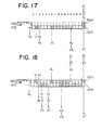
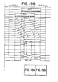
- signals CNTEN1 (1901) and CNTEN2 (1902) respectively enable counting operation of the address counters A 111 and B 117 shown in Fig. 7.
- a signal 1903 represents the output of the address counter A 111 initiating the counting operation by said CNTEN1 signal, and is supplied, as a memory address to the line buffer memory A 112 shown in Fig. 7.
- a signal 1904 represents the memory address of the line buffer memory a in Fig. 7.
- Signals 908, 910, 909 and 911 are input and output signals of the shift registers A 115 and B 116 shown in Fig. 7, and have waveforms corresponding to the image shown in Fig. 15.
- the buffer memories A 112 and B .113 shown in Fig. 7 alternatively perform reading and writing operations in such a manner that the reading said always precedes by a period corresponding to five clocks, since the decoding of code data is rendered possible only when the information on the changing point and color for the first pixel of the reference line reaches the output Q4 of the shift registers B116 and A 115 shown in Fig. 7.
- the number of clocks can be made other than 5, however, by the suitable selection of the number of bits of the shift register or the number of timing latches for decording operation.
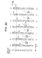
- Fig. 20 shows the displacement of bodes in the register C 103 in the decoding of the first line 1502 shown in Fig. 15..
- the HSYNC1 signal shown in Fig. 19 triggers the decoding operation, thus initiating the reading operation in the buffer memory A shown in Fig. 7.
- the buffer memory A release the data of a reference line in this state, and, according to the encoding rule, the hypothetical line of all white is read as the reference line for decoding the first line. In this manner, in the initial state, the content of the buffer memory A is cleared to all zero.
- a first terminating code of H-mode which is the Wl code in this case, has been detected. Since the Wl code has a code length of 6 and is a jump code as explained before, the register C effects a jump shift of 6 bits in a clock timing. Since the Wl code is a terminating code, the flip-flop 1403 shown in Fig. 14 is set by the signal M/T simultaneously with the loading of said run length, thus memorizing a fact that the terminator value is loaded in the run length counter 602 (signal 1908 in Fi g . 19).
- the register C assumes a state shown in Fig. 20(B), achieved by a 6-bit shift from the state at the time t-1. Then the TEND signal 1404 shown in Fig. 14, is released to invert the output of the flip-flop 1401, at a time tl after t0 by a clock, and the color of the changes from white to black as shown by 1910 in Fig. 19.
- a BlH code is detected (second terminating code in the H-mode) from the output signals C3 - C6 of the register C 103 in the state of Fig. 20(B), in response to the TEND signal corresponding to the HCRO signal.
- the B1H code has a run length 1 (compliment (-1)), a code length 3 and is a jump code.
- (-1) is loaded again in the run length counter 602.
- the decoding operation of the H-mode code is completed, and a succeeding mode is decoded.
- the register C 103 performs a jump shift of 6 bits, which is equal to the sum of the code length 3 of the B1H code and the code length 3 of the H-code, in order to position the leading bit of the succeeding code at the output CO of the register C 103, whereby reached is the state shown in Fig. 20(C).
- the HCRO signal at the time tl inverts the flip-flop 1404 in Fig. 14, at a time t2.
- a B6 code is detected from the register C 103 of a state shown in Fig. 20(D).
- the B6 code has a code length of 4 and is not a jump code.
- the register C 103 performs a stepwise displacement from the time t5 and reaches a state shown in Fig. 20(E) at time t9.
- the B6 code has been detected as a second terminating code in the H-mode, and is further subjected to a 3-bit jump shift at the time t9, in order to position the leading end of a succeeding code at the output CO of the register C 103.
- the register C 103 assumes a state shown in Fig. 20(F) at a time tlO.
- the HCRO signal is released at a time tll, whereby the flip-flop 1401 shown in Fig. 14 is inverted and, from the register C 103, there is detected a succeeding code, which is a V(0) code in the V-mode.
- a signal "1" is set in the V(0) bit of the latch 301 in Fig. 12, while other bits remain as "0". Since the H-mode is not assumed in this state, the run length counter 602 in Fig. 6 is not activated, and the HCRO signal is not released.
- Said V(0) bit of the latch 301 is compared, in the PV reference circuit 105, with the symbol bl from the AND gate 704 receiving the output B4 of the shift register B 116 shown in Fig.
- the flip-flop 1401 shown in Fig. 14 is inverted. In this manner there is regenerated an image as represented by 1901 in Fig. 19.
- the effective period of the regenerated image is indicated by signal 1914 shown in Fig. 19.
- the image 1910 is supplied to the printer 119, and also stored in the line buffer B 113 which is in a parallel writing operation, for use as the reference line for decoding of the second line. Said regenerated image is also used as the symbol a0. The regeneration or decoding of the image is conducted in this manner.
- various circuit blocks of the present embodiment receive common image clock signals from the control circuit 118 shown in Fig. 1, and the decoding operation is conducted in synchronization with said image clock signals, at a speed corresponding to the interval of the clock signals.
- the decoding operation is interrupted if the supply of said clock signals is interrupted for a period. It is therefore rendered possible to control the speed of decoding operation, by regulating the frequency of the clock signals commonly supplied to the various blocks of the decoding circuit.
- the decoding operation can be conducted with a speed matching the processing speed of a succeeding device, such as a printer, by utilizing clock signals synchronized with the speed of said printer. Consequently a decoding circuit can be commonly used for plural printers of different processing speeds. Also in case such succeeding device functions intermittently as in a computer, the decoding operation can also be conducted intermittently by supplying the clock signals only during the data fetching period and interrupting the supply of clock signals in other periods.
- a high-speed decoding operation can be achieved without delay in the decoding of two-dimensionally encoded image codes such as obtained by MR or MMR encoding, since a horizontal-mode identification code and a succeeding run length code are simultaneously discriminated.
- a high-speed decoding operation can be achieved in the decoding of two-dimensionally encoded image codes such as obtained by MR or MMR encoding, since, in the horizontal mode, a run length code can be decoded without the release of a preceding horizontal-mode identification code.
- a high-speed decoding operation can be achieved with satisfactory accuracy, since the decoding operation is initiated after there are fetched image signals of the reference line of a number of pixels necessary for the decoding of image codes.
Landscapes
- Engineering & Computer Science (AREA)
- Theoretical Computer Science (AREA)
- Multimedia (AREA)
- Signal Processing (AREA)
- Compression Of Band Width Or Redundancy In Fax (AREA)
- Compression, Expansion, Code Conversion, And Decoders (AREA)
- Image Processing (AREA)
Applications Claiming Priority (12)
| Application Number | Priority Date | Filing Date | Title |
|---|---|---|---|
| JP17531085A JPS6235779A (ja) | 1985-08-08 | 1985-08-08 | 画像コ−ドの復号装置 |
| JP175308/85 | 1985-08-08 | ||
| JP175310/85 | 1985-08-08 | ||
| JP17530885A JP2774489B2 (ja) | 1985-08-08 | 1985-08-08 | 画像コードの復号装置 |
| JP175307/85 | 1985-08-08 | ||
| JP175306/85 | 1985-08-08 | ||
| JP17530785A JPS6235776A (ja) | 1985-08-08 | 1985-08-08 | 画像コ−ドの復号装置 |
| JP17530985A JPS6235778A (ja) | 1985-08-08 | 1985-08-08 | 画像コ−ドの復号装置 |
| JP175309/85 | 1985-08-08 | ||
| JP17530685A JP2774488B2 (ja) | 1985-08-08 | 1985-08-08 | 画像コードの復号装置 |
| JP175311/85 | 1985-08-08 | ||
| JP17531185A JP2774490B2 (ja) | 1985-08-08 | 1985-08-08 | 画像コードの復号装置 |
Publications (3)
| Publication Number | Publication Date |
|---|---|
| EP0212905A2 true EP0212905A2 (fr) | 1987-03-04 |
| EP0212905A3 EP0212905A3 (en) | 1988-07-20 |
| EP0212905B1 EP0212905B1 (fr) | 1994-06-08 |
Family
ID=27553435
Family Applications (1)
| Application Number | Title | Priority Date | Filing Date |
|---|---|---|---|
| EP86306006A Expired - Lifetime EP0212905B1 (fr) | 1985-08-08 | 1986-08-04 | Appareil pour décoder des codes d'image |
Country Status (5)
| Country | Link |
|---|---|
| US (1) | US4750043A (fr) |
| EP (1) | EP0212905B1 (fr) |
| CN (1) | CN1008501B (fr) |
| CA (1) | CA1259414A (fr) |
| DE (1) | DE3689893T2 (fr) |
Cited By (1)
| Publication number | Priority date | Publication date | Assignee | Title |
|---|---|---|---|---|
| EP0493086A3 (en) * | 1990-12-24 | 1993-05-19 | Xerox Corporation | Data decoding apparatus |
Families Citing this family (10)
| Publication number | Priority date | Publication date | Assignee | Title |
|---|---|---|---|---|
| US4887224A (en) * | 1986-08-28 | 1989-12-12 | Canon Kabushiki Kaisha | Image data processing apparatus capable of high-speed data encoding and/or decoding |
| JPS63138881A (ja) * | 1986-11-29 | 1988-06-10 | Hitachi Ltd | Mr符号伸長装置 |
| EP0624970B1 (fr) * | 1989-09-04 | 1998-11-25 | Canon Kabushiki Kaisha | Dispositif de fac-similé |
| EP0469716B1 (fr) * | 1990-07-03 | 1997-04-23 | Canon Kabushiki Kaisha | Appareil à traitement pour images |
| JP3066909B2 (ja) * | 1990-08-27 | 2000-07-17 | キヤノン株式会社 | 復号装置 |
| JP2794951B2 (ja) * | 1990-12-17 | 1998-09-10 | 村田機械株式会社 | Mr符号の復号化方法 |
| US5229863A (en) * | 1990-12-24 | 1993-07-20 | Xerox Corporation | High speed CCITT decompressor |
| JPH05130434A (ja) * | 1991-10-31 | 1993-05-25 | Canon Inc | 画像圧縮装置 |
| JP2004334295A (ja) * | 2003-04-30 | 2004-11-25 | Yamaha Corp | 記憶装置 |
| CN1330720C (zh) * | 2005-06-16 | 2007-08-08 | 武汉科利尔化工有限公司 | 水基聚氨酯树脂及其电泳漆组合物和制备方法 |
Citations (1)
| Publication number | Priority date | Publication date | Assignee | Title |
|---|---|---|---|---|
| US4156880A (en) | 1976-06-28 | 1979-05-29 | Nippon Telegraph And Telephone Public Corporation | Method for transmitting a facsimile signal by sequential edge differential coding |
Family Cites Families (7)
| Publication number | Priority date | Publication date | Assignee | Title |
|---|---|---|---|---|
| US3941922A (en) * | 1972-11-15 | 1976-03-02 | Matsushita Electric Industrial Co., Ltd. | Facsimile system of run-length |
| DE2458119C3 (de) * | 1974-12-09 | 1980-08-14 | Siemens Ag, 1000 Berlin Und 8000 Muenchen | Verfahren und Anordnung zur Faksimilecodierung |
| JPS5812787B2 (ja) * | 1975-10-16 | 1983-03-10 | ケイディディ株式会社 | フアクシミリシンゴウノジユシンホウシキ |
| JPS53134340A (en) * | 1977-04-28 | 1978-11-22 | Ricoh Co Ltd | Run length coding system |
| JPS54153516A (en) * | 1978-05-25 | 1979-12-03 | Ricoh Co Ltd | Data processing system for facsimile |
| FR2430139A1 (fr) * | 1978-06-28 | 1980-01-25 | Labo Electronique Physique | Dispositif de compression de signaux binaires et systeme de transmission codee de fac-similes equipe de ce dispositif |
| US4610027A (en) * | 1983-12-30 | 1986-09-02 | International Business Machines Corporation | Method for converting a bit map of an image to a run length or run end representation |
-
1986
- 1986-08-04 EP EP86306006A patent/EP0212905B1/fr not_active Expired - Lifetime
- 1986-08-04 US US06/892,114 patent/US4750043A/en not_active Expired - Lifetime
- 1986-08-04 DE DE3689893T patent/DE3689893T2/de not_active Expired - Lifetime
- 1986-08-06 CA CA000515412A patent/CA1259414A/fr not_active Expired
- 1986-08-07 CN CN86106162A patent/CN1008501B/zh not_active Expired
Patent Citations (1)
| Publication number | Priority date | Publication date | Assignee | Title |
|---|---|---|---|---|
| US4156880A (en) | 1976-06-28 | 1979-05-29 | Nippon Telegraph And Telephone Public Corporation | Method for transmitting a facsimile signal by sequential edge differential coding |
Non-Patent Citations (3)
| Title |
|---|
| "Red Book", vol. VII, 18 October 1984, pages: 16 - 48 |
| RED BOOK, vol. VII, 8 October 1984 (1984-10-08), pages 16 - 48 |
| YOSHIDA ET AL.: "Development of Compressor and Expander for 1 second facsimile", 2311 FUJITSU SCIENTIFIC AND TECHNICAL JOURNAL, vol. 19, no. 3, September 1983 (1983-09-01), pages 323 |
Cited By (1)
| Publication number | Priority date | Publication date | Assignee | Title |
|---|---|---|---|---|
| EP0493086A3 (en) * | 1990-12-24 | 1993-05-19 | Xerox Corporation | Data decoding apparatus |
Also Published As
| Publication number | Publication date |
|---|---|
| EP0212905A3 (en) | 1988-07-20 |
| CN1008501B (zh) | 1990-06-20 |
| CA1259414A (fr) | 1989-09-12 |
| DE3689893T2 (de) | 1994-11-03 |
| DE3689893D1 (de) | 1994-07-14 |
| US4750043A (en) | 1988-06-07 |
| CN86106162A (zh) | 1987-04-29 |
| EP0212905B1 (fr) | 1994-06-08 |
Similar Documents
| Publication | Publication Date | Title |
|---|---|---|
| US4500926A (en) | Data-recording apparatus | |
| US4800441A (en) | Binary data compression and expansion processing apparatus | |
| CA1119303A (fr) | Transmission et/ou enregistrement de signaux numeriques | |
| US4131915A (en) | Facsimile signal transmission system | |
| US4376933A (en) | Circuit for compacting data | |
| US5022088A (en) | Image processing apparatus with provision for memory operation | |
| US4750043A (en) | Decoding apparatus for image code | |
| US4134133A (en) | Method for interline-coding facsimile signal | |
| US4760461A (en) | Binary data compression and expansion processing apparatus | |
| US4654719A (en) | Coding circuit for facsimile apparatus | |
| US4758899A (en) | Data compression control device | |
| US4716471A (en) | Data decoding apparatus | |
| CA1291822C (fr) | Methode et dispositif de tratiement d'un signal d'image | |
| US5345316A (en) | Image data encoding/decoding apparatus for concurrent processing of multiple image data streams | |
| US5577182A (en) | Image processing apparatus | |
| US4837634A (en) | Apparatus for decoding image codes obtained by compression process | |
| EP0751675A2 (fr) | Appareil de formation d'image | |
| EP0149893A1 (fr) | Appareil pour coder et décoder des données | |
| US4338637A (en) | Variable scanning device | |
| JP2774490B2 (ja) | 画像コードの復号装置 | |
| EP0667619B1 (fr) | Appareil de traitement de l'information | |
| JP2774489B2 (ja) | 画像コードの復号装置 | |
| JPS6333350B2 (fr) | ||
| JPH0145270B2 (fr) | ||
| JPH06205229A (ja) | 符号化装置 |
Legal Events
| Date | Code | Title | Description |
|---|---|---|---|
| PUAI | Public reference made under article 153(3) epc to a published international application that has entered the european phase |
Free format text: ORIGINAL CODE: 0009012 |
|
| AK | Designated contracting states |
Kind code of ref document: A2 Designated state(s): BE DE FR GB NL SE |
|
| PUAL | Search report despatched |
Free format text: ORIGINAL CODE: 0009013 |
|
| AK | Designated contracting states |
Kind code of ref document: A3 Designated state(s): BE DE FR GB NL SE |
|
| 17P | Request for examination filed |
Effective date: 19881219 |
|
| 17Q | First examination report despatched |
Effective date: 19901010 |
|
| GRAA | (expected) grant |
Free format text: ORIGINAL CODE: 0009210 |
|
| AK | Designated contracting states |
Kind code of ref document: B1 Designated state(s): BE DE FR GB NL SE |
|
| REF | Corresponds to: |
Ref document number: 3689893 Country of ref document: DE Date of ref document: 19940714 |
|
| ET | Fr: translation filed | ||
| EAL | Se: european patent in force in sweden |
Ref document number: 86306006.7 |
|
| PLBE | No opposition filed within time limit |
Free format text: ORIGINAL CODE: 0009261 |
|
| STAA | Information on the status of an ep patent application or granted ep patent |
Free format text: STATUS: NO OPPOSITION FILED WITHIN TIME LIMIT |
|
| 26N | No opposition filed | ||
| REG | Reference to a national code |
Ref country code: GB Ref legal event code: IF02 |
|
| PGFP | Annual fee paid to national office [announced via postgrant information from national office to epo] |
Ref country code: GB Payment date: 20050721 Year of fee payment: 20 |
|
| PGFP | Annual fee paid to national office [announced via postgrant information from national office to epo] |
Ref country code: NL Payment date: 20050815 Year of fee payment: 20 |
|
| PGFP | Annual fee paid to national office [announced via postgrant information from national office to epo] |
Ref country code: FR Payment date: 20050819 Year of fee payment: 20 |
|
| PGFP | Annual fee paid to national office [announced via postgrant information from national office to epo] |
Ref country code: SE Payment date: 20050823 Year of fee payment: 20 |
|
| PGFP | Annual fee paid to national office [announced via postgrant information from national office to epo] |
Ref country code: BE Payment date: 20050915 Year of fee payment: 20 |
|
| PGFP | Annual fee paid to national office [announced via postgrant information from national office to epo] |
Ref country code: DE Payment date: 20051024 Year of fee payment: 20 |
|
| PG25 | Lapsed in a contracting state [announced via postgrant information from national office to epo] |
Ref country code: GB Free format text: LAPSE BECAUSE OF EXPIRATION OF PROTECTION Effective date: 20060803 |
|
| PG25 | Lapsed in a contracting state [announced via postgrant information from national office to epo] |
Ref country code: NL Free format text: LAPSE BECAUSE OF EXPIRATION OF PROTECTION Effective date: 20060804 |
|
| REG | Reference to a national code |
Ref country code: GB Ref legal event code: PE20 |
|
| NLV7 | Nl: ceased due to reaching the maximum lifetime of a patent |
Effective date: 20060804 |
|
| EUG | Se: european patent has lapsed | ||
| BE20 | Be: patent expired |
Owner name: *CANON K.K. Effective date: 20060804 |