EP0213647B1 - Détecteur de phase - Google Patents
Détecteur de phase Download PDFInfo
- Publication number
- EP0213647B1 EP0213647B1 EP86201067A EP86201067A EP0213647B1 EP 0213647 B1 EP0213647 B1 EP 0213647B1 EP 86201067 A EP86201067 A EP 86201067A EP 86201067 A EP86201067 A EP 86201067A EP 0213647 B1 EP0213647 B1 EP 0213647B1
- Authority
- EP
- European Patent Office
- Prior art keywords
- signal
- flipflop
- detection
- phase detector
- data
- Prior art date
- Legal status (The legal status is an assumption and is not a legal conclusion. Google has not performed a legal analysis and makes no representation as to the accuracy of the status listed.)
- Expired
Links
- 238000001514 detection method Methods 0.000 claims abstract description 39
- 238000005259 measurement Methods 0.000 claims abstract description 7
- 230000005540 biological transmission Effects 0.000 claims abstract description 4
- 238000010586 diagram Methods 0.000 description 6
- 238000013500 data storage Methods 0.000 description 1
- 230000001934 delay Effects 0.000 description 1
- 230000001419 dependent effect Effects 0.000 description 1
- 238000001914 filtration Methods 0.000 description 1
Images


Classifications
-
- H—ELECTRICITY
- H03—ELECTRONIC CIRCUITRY
- H03D—DEMODULATION OR TRANSFERENCE OF MODULATION FROM ONE CARRIER TO ANOTHER
- H03D13/00—Circuits for comparing the phase or frequency of two mutually-independent oscillations
- H03D13/003—Circuits for comparing the phase or frequency of two mutually-independent oscillations in which both oscillations are converted by logic means into pulses which are applied to filtering or integrating means
- H03D13/004—Circuits for comparing the phase or frequency of two mutually-independent oscillations in which both oscillations are converted by logic means into pulses which are applied to filtering or integrating means the logic means delivering pulses at more than one terminal, e.g. up and down pulses
Definitions
- This invention relates to a phase detector for generating a measurement signal indicating the extent to which the actual distance ⁇ between the flanks of data pulses generated for serial data transmission and the detection times determined by a detection clock differs from a required distance Tg, in which phase detector, after detection of a flank of a data pulse, a detection signal phase is generated whose pulse width corresponds to the said actual distance c, for which purpose the phase detector is provided with a first D-flipflop controlled by the detection clock and an exclusive OR-gate, the data pulses being fed to the D-input of the first flipflop and the the first input of the exclusive OR-gate, while the output signal of the D-flipflop functioning as detected data is fed to the second input of the exclusive OR-gate, and the detection signal is generated at the output of the exclusive OR-gate, in which phase detector, again after detection of a flank of a data pulse, by means of a second D-flipflop, a reference signal pulse is generated whose pulse width is derived from the detection signal, which width is a
- a phase detector of this kind is known from European patent application No. EP-A 0 0 54 322.
- a reference pulse is delivered whose width is equal to half the clock cycle time.
- the reference signal is fed to a controlled current source, which current source generates a first current.
- the detection signal is also fed to a second controlled current source, which generates a second current whose value is equal to the first current.
- the first current is subtracted from the second current and the differential current is a measure of the difference between the actual distance and the required distance.
- the output of the first flipflop is connected to the input of the second flipflop.
- the second flipflop is controlled by a clock signal 180 ° phase-shifted with respect to the phase of the clock signal of the control for the first flipflop.
- the second flipflop output signal is shifted with respect to the first flipflop output signal.
- Both the output of the first flipflop and the output of the second flipflop are fed to an exclusive OR-gate, which generates a reference pulse at each flank of a data pulse.
- the width of the reference pulse depends on the clock signal duty-cycle. In the case of a reference signal pulse width equal to half the cycle time of a clock signal a duty-cycle of 50% is required.
- the object of the invention is to provide a phase detector whose proper operation is independent of the duty-cycle of the clock signal supplied.
- this object is attained in that the D-input of the second flipflop is connected to the output of the exclusive OR-gate, in that the clock inputs of the first flipflop and second flipflop are directly interconnected, in that the output signal of the second flipflop functions as a reference signal, and in that the phase detector is provided with at least one adjustment circuit, by means of which the amplitude of the detection signal and/or of the reference signal is/are so adjusted before the signals are fed to the subtraction circuit that the ratio between the amplitude of the reference signal and the amplitude of the detection signal after adjustment is equal to Tg/T.
- a reference signal of a width equal to the clock signal cycle time is always fed to the output of the second flipflop.
- the flipflop for determining the reference pulse is controlled by the same clock signal as the first flipflop, so that proper operation of the phase detector is obtained irrespective of the clock signal duty- cylce.
- the second exclusive OR-gate used in the prior art phase detector has become superfluous for generation of the reference pulse.
- the data input signal Din is fed to a flank detector circuit 1 which delivers a signal pulse if a flank is detected.
- the signal is then fed to a one-shot circuit 2.
- a multiplier acting as phase detection element 3 the phase of the date signal is compared with the regenerated clock originating from the oscillator 5.
- the control voltage obtained from this phase detection element is fed via the loop filter 4 to the voltage controlled oscillator (VCO) 5 which is tuned to the clock frequency.
- VCO voltage controlled oscillator
- An extra (adjustable) delay circuit 6 is often required, as a result of the non-linear processing in 1 and the phase detection in 3 and, possibly, as a result of time delays, to position the phase of the regenerated clock fcL in the middle of the bit cell for the purpose of optimum detection of the data in the circuit 7. Since both circuit 1 and circuit 6 are frequency- dependent, frequency deviations may also cause deviations in the detection time.
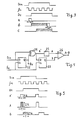
- Fig. 2 represents a phase detector which adjusts the phase of the regenerated clock to the middle of the bit cell by making the distance ⁇ 1 between a flank in the data and the following detection time (positive clock flank) equal to the distance ⁇ 2 between the following flank and the proceeding detection time (positive clock flank).
- This embodiment has two D-type flipflops 11, 12 twoo AND-gates 13, 14, an OR-gate 15 and a differential amplifier 16.
- Fig. 3 represents some waveforms of signals occurring in the phase detector of Fig. 2.
- the data input signal Din is fed to the D-input of the flipflop 11 and to the AND-gates 13, 14.
- the clock fc L regenerated by the phase-lock-loop oscillator is fed to the clock input CL of the flipflop 11, and flipflop 12 respectively.
- the data signal D ⁇ to be regarded as the detected data is fed from the Q(set) output of 11 to the AND-gate 14 and the signal inverted with respect to D ⁇ is fed from the Q (reset) output to the AND-gate 13.
- the output signal b of the AND-gate 14 is fed to the D input of the flipflop 12 and to the minus input of the differential amplifier 16.
- the Q output signal c of the flipflop 12 and the output signal a of the AND-gate 13 are fed to the two inputs of the OR-gate 15.
- the output signal a + c thereof is fed to the plus input of the differential amplifier 16.
- This control voltage is fed to the loop filter.
- the control is such that ⁇ 1 is made equal to ⁇ 2 , in which case the optimum detection time then falls exactly in the middle of the data bit cell. In these conditions the phase information is obtained from two consecutive flanks, i.e. a positive flank and a negative flank, of the data.
- Fig. 4 represents the phase detector according to the invention, in which a complete phase measurement is carried out for each flank in the data.
- the distance between a flank in the data and the following detection time is made equal to half the clock time T.
- this phase detector according to the invention always measures both the said distance and the clock cycle time T.
- the phase detector in Fig. 4 is constructed of just a few elements, i.e. two D-type flipflops 22, 23, an exclusive OR-gate 24, a factor-2 multiplier 25, and a differential amplifier 26.
- Fig. 5 represents some waveforms of signals occurring in the phase detector of Fig. 4.
- the data input signal Di n is fed to the D-input of the flipflop 22 and to one input of the exclusive OR-gate 24.
- This clock fc L regenerated by the loop oscillator is fed to the clock inputs CL of both flipflops 22, 23.
- the data signal D ⁇ taken from the Q(set) output is fed to the other input of the OR-gate 24.
- the output signal A' thereof is fed to the multiplier 25 and to the D-input of the flipflop 23.
- the output signal A of multiplier 25 and the output signal B of the Q-output of the flipflop 23 are fed to the plus input, and the minus input respectively of the differential amplier 26.
- Figs. 6a and 6b represent a practical embodiment of the phase detector illustrated in Fig. 4.
- Fig. 6a includes a plurality of inverters used to form the reference voltage V ref and the other input signal A + B for the differential amplifier 26 (see Fig. 6b).
- Fig. 6b represents how the factor-2 multiplier is constructed by means of a diode F and a resistor Ro. This resistor Ro is switched in only during the inverted pulse ⁇ . Ro is smaller than the resistance R of the other resistors as a result of the voltage drop across the diode F during the pulse T . From the output of the differential amplifier 26 the control voltage is fed to the loop filter.
- phase detector according to the invention.
- the advantages of this phase detector according to the invention are the high reliability of data detection and the small number of components required. Despite the presence of noise or jitter on the flanks, optimum detection is at all times obtained in the middle of the data bit cell, optimum use being made of the clock information present in the data and a complete phase measurement is carried out at each flank in the data.
- the lock-in range of the phase-lock-loop is also improved, i.e. the loop oscillator can have a somewhat greater relative deviation in frequency and yet the loop can still lock. At the same time the risk of false locking is reduced.
- this phase detector can also be used for data processing requiring bit synchronization, such as for data storage.
Landscapes
- Engineering & Computer Science (AREA)
- Power Engineering (AREA)
- Stabilization Of Oscillater, Synchronisation, Frequency Synthesizers (AREA)
- Radar Systems Or Details Thereof (AREA)
- Synchronisation In Digital Transmission Systems (AREA)
- Investigating Or Analyzing Materials By The Use Of Ultrasonic Waves (AREA)
- Investigating Or Analyzing Materials By The Use Of Magnetic Means (AREA)
Claims (1)
Priority Applications (1)
| Application Number | Priority Date | Filing Date | Title |
|---|---|---|---|
| AT86201067T ATE47259T1 (de) | 1985-07-01 | 1986-06-19 | Phasendetektor. |
Applications Claiming Priority (2)
| Application Number | Priority Date | Filing Date | Title |
|---|---|---|---|
| NL8501887 | 1985-07-01 | ||
| NL8501887A NL8501887A (nl) | 1985-07-01 | 1985-07-01 | Fasedetector. |
Publications (2)
| Publication Number | Publication Date |
|---|---|
| EP0213647A1 EP0213647A1 (fr) | 1987-03-11 |
| EP0213647B1 true EP0213647B1 (fr) | 1989-10-11 |
Family
ID=19846229
Family Applications (1)
| Application Number | Title | Priority Date | Filing Date |
|---|---|---|---|
| EP86201067A Expired EP0213647B1 (fr) | 1985-07-01 | 1986-06-19 | Détecteur de phase |
Country Status (6)
| Country | Link |
|---|---|
| US (1) | US4749937A (fr) |
| EP (1) | EP0213647B1 (fr) |
| JP (1) | JPS6243235A (fr) |
| AT (1) | ATE47259T1 (fr) |
| DE (1) | DE3666316D1 (fr) |
| NL (1) | NL8501887A (fr) |
Families Citing this family (3)
| Publication number | Priority date | Publication date | Assignee | Title |
|---|---|---|---|---|
| IT1236578B (it) * | 1989-07-04 | 1993-03-16 | Ind Face Standard S P A Milano | Dispositivo per la trasformazione di un flip flop di tipo d in un flip flop denominato di tipo b in grado di campionare i dati sui fronti di salita e sui fronti di discesa del segnale di clock. |
| JPH04250712A (ja) * | 1991-01-25 | 1992-09-07 | Toshiba Corp | 半導体集積回路 |
| CN1068473C (zh) * | 1994-04-07 | 2001-07-11 | Rca.汤姆森许可公司 | 锁相环的鉴相器 |
Family Cites Families (5)
| Publication number | Priority date | Publication date | Assignee | Title |
|---|---|---|---|---|
| US4222009A (en) * | 1978-11-02 | 1980-09-09 | Sperry Corporation | Phase lock loop preconditioning circuit |
| DE3171263D1 (en) * | 1980-12-12 | 1985-08-08 | Philips Electronic Associated | Phase sensitive detector |
| JPS58182938A (ja) * | 1982-04-21 | 1983-10-26 | Toshiba Corp | Pll形タイミング抽出回路 |
| US4599570A (en) * | 1982-07-21 | 1986-07-08 | Sperry Corporation | Phase detector with independent offset correction |
| US4668917A (en) * | 1984-01-03 | 1987-05-26 | Motorola, Inc. | Phase comparator for use with a digital phase locked loop or other phase sensitive device |
-
1985
- 1985-07-01 NL NL8501887A patent/NL8501887A/nl not_active Application Discontinuation
-
1986
- 1986-06-19 DE DE8686201067T patent/DE3666316D1/de not_active Expired
- 1986-06-19 AT AT86201067T patent/ATE47259T1/de not_active IP Right Cessation
- 1986-06-19 EP EP86201067A patent/EP0213647B1/fr not_active Expired
- 1986-06-27 US US06/879,377 patent/US4749937A/en not_active Expired - Fee Related
- 1986-06-30 JP JP61153949A patent/JPS6243235A/ja active Pending
Also Published As
| Publication number | Publication date |
|---|---|
| EP0213647A1 (fr) | 1987-03-11 |
| JPS6243235A (ja) | 1987-02-25 |
| NL8501887A (nl) | 1987-02-02 |
| ATE47259T1 (de) | 1989-10-15 |
| US4749937A (en) | 1988-06-07 |
| DE3666316D1 (en) | 1989-11-16 |
Similar Documents
| Publication | Publication Date | Title |
|---|---|---|
| EP0709966B1 (fr) | Détecteur de phase à sortie ternaire | |
| US4371974A (en) | NRZ Data phase detector | |
| US4587496A (en) | Fast acquisition phase-lock loop | |
| EP0502739A2 (fr) | Système de récupération de données et d'horloge NRZ utilisant une boucle à verrouillage de phase | |
| US4338569A (en) | Delay lock loop | |
| GB2180708A (en) | Phase-comparator lock-detect circuit for a frequency synthesiser | |
| US4473805A (en) | Phase lock loss detector | |
| EP0094837A2 (fr) | Circuit à boucle d'asservissement de phase à capacité de verrouillage | |
| EP0800061A2 (fr) | Débitmètre à vortex | |
| JPS6340370B2 (fr) | ||
| GB2067371A (en) | Phase lock system | |
| EP0277726A2 (fr) | Boucles d'asservissement de phase | |
| US5956379A (en) | Digital phase lock detector and low-pass filter selector | |
| US4575684A (en) | Differential phase shift keying receiver | |
| US4849704A (en) | Duty cycle independent phase detector | |
| US4080576A (en) | Tow mode harmonic and nonharmonic phase detector | |
| US6757349B1 (en) | PLL frequency synthesizer with lock detection circuit | |
| US4843332A (en) | Wide range digital phase/frequency detector | |
| US5469478A (en) | Digital phase lock loop for jitter filtering and frequency offset compensation | |
| US4801896A (en) | Circuit providing improved lock-in for a phase-locked loop | |
| EP1006660B1 (fr) | Appareil d'identification et de reproduction de signal d'horloge | |
| EP0213647A1 (fr) | Détecteur de phase | |
| GB2161662A (en) | Phase synchronisation circuit | |
| CN113541915B (zh) | 一种宽动态范围的快速时钟恢复实现方法及装置 | |
| US7183863B1 (en) | Self-initializing frequency detector |
Legal Events
| Date | Code | Title | Description |
|---|---|---|---|
| PUAI | Public reference made under article 153(3) epc to a published international application that has entered the european phase |
Free format text: ORIGINAL CODE: 0009012 |
|
| AK | Designated contracting states |
Kind code of ref document: A1 Designated state(s): AT BE CH DE FR GB IT LI NL SE |
|
| 17P | Request for examination filed |
Effective date: 19870807 |
|
| 17Q | First examination report despatched |
Effective date: 19881122 |
|
| GRAA | (expected) grant |
Free format text: ORIGINAL CODE: 0009210 |
|
| AK | Designated contracting states |
Kind code of ref document: B1 Designated state(s): AT BE CH DE FR GB IT LI NL SE |
|
| REF | Corresponds to: |
Ref document number: 47259 Country of ref document: AT Date of ref document: 19891015 Kind code of ref document: T |
|
| REF | Corresponds to: |
Ref document number: 3666316 Country of ref document: DE Date of ref document: 19891116 |
|
| ET | Fr: translation filed | ||
| ITF | It: translation for a ep patent filed | ||
| PGFP | Annual fee paid to national office [announced via postgrant information from national office to epo] |
Ref country code: FR Payment date: 19900510 Year of fee payment: 5 Ref country code: AT Payment date: 19900510 Year of fee payment: 5 |
|
| PGFP | Annual fee paid to national office [announced via postgrant information from national office to epo] |
Ref country code: GB Payment date: 19900515 Year of fee payment: 5 |
|
| PGFP | Annual fee paid to national office [announced via postgrant information from national office to epo] |
Ref country code: SE Payment date: 19900516 Year of fee payment: 5 |
|
| PGFP | Annual fee paid to national office [announced via postgrant information from national office to epo] |
Ref country code: BE Payment date: 19900518 Year of fee payment: 5 |
|
| PGFP | Annual fee paid to national office [announced via postgrant information from national office to epo] |
Ref country code: CH Payment date: 19900522 Year of fee payment: 5 |
|
| PGFP | Annual fee paid to national office [announced via postgrant information from national office to epo] |
Ref country code: DE Payment date: 19900530 Year of fee payment: 5 |
|
| ITTA | It: last paid annual fee | ||
| PGFP | Annual fee paid to national office [announced via postgrant information from national office to epo] |
Ref country code: NL Payment date: 19900630 Year of fee payment: 5 |
|
| PLBE | No opposition filed within time limit |
Free format text: ORIGINAL CODE: 0009261 |
|
| STAA | Information on the status of an ep patent application or granted ep patent |
Free format text: STATUS: NO OPPOSITION FILED WITHIN TIME LIMIT |
|
| 26N | No opposition filed | ||
| PG25 | Lapsed in a contracting state [announced via postgrant information from national office to epo] |
Ref country code: GB Effective date: 19910619 Ref country code: AT Effective date: 19910619 |
|
| PG25 | Lapsed in a contracting state [announced via postgrant information from national office to epo] |
Ref country code: SE Effective date: 19910620 |
|
| PG25 | Lapsed in a contracting state [announced via postgrant information from national office to epo] |
Ref country code: LI Effective date: 19910630 Ref country code: CH Effective date: 19910630 Ref country code: BE Effective date: 19910630 |
|
| BERE | Be: lapsed |
Owner name: OCE-NEDERLAND B.V. Effective date: 19910630 |
|
| PG25 | Lapsed in a contracting state [announced via postgrant information from national office to epo] |
Ref country code: NL Effective date: 19920101 |
|
| GBPC | Gb: european patent ceased through non-payment of renewal fee | ||
| NLV4 | Nl: lapsed or anulled due to non-payment of the annual fee | ||
| PG25 | Lapsed in a contracting state [announced via postgrant information from national office to epo] |
Ref country code: FR Effective date: 19920228 |
|
| REG | Reference to a national code |
Ref country code: CH Ref legal event code: PL |
|
| PG25 | Lapsed in a contracting state [announced via postgrant information from national office to epo] |
Ref country code: DE Effective date: 19920401 |
|
| REG | Reference to a national code |
Ref country code: FR Ref legal event code: ST |
|
| EUG | Se: european patent has lapsed |
Ref document number: 86201067.5 Effective date: 19920109 |
|
| PG25 | Lapsed in a contracting state [announced via postgrant information from national office to epo] |
Ref country code: IT Free format text: LAPSE BECAUSE OF NON-PAYMENT OF DUE FEES;WARNING: LAPSES OF ITALIAN PATENTS WITH EFFECTIVE DATE BEFORE 2007 MAY HAVE OCCURRED AT ANY TIME BEFORE 2007. THE CORRECT EFFECTIVE DATE MAY BE DIFFERENT FROM THE ONE RECORDED. Effective date: 20050619 |