EP0215213A1 - Herstellungsverfahren von Hoch- und Niederspannungstransistoren unter Verwendung von epitaktischen Schichten gleichmässiger Dicke - Google Patents
Herstellungsverfahren von Hoch- und Niederspannungstransistoren unter Verwendung von epitaktischen Schichten gleichmässiger Dicke Download PDFInfo
- Publication number
- EP0215213A1 EP0215213A1 EP86108988A EP86108988A EP0215213A1 EP 0215213 A1 EP0215213 A1 EP 0215213A1 EP 86108988 A EP86108988 A EP 86108988A EP 86108988 A EP86108988 A EP 86108988A EP 0215213 A1 EP0215213 A1 EP 0215213A1
- Authority
- EP
- European Patent Office
- Prior art keywords
- transistor
- epitaxial layer
- region
- base
- collector
- Prior art date
- Legal status (The legal status is an assumption and is not a legal conclusion. Google has not performed a legal analysis and makes no representation as to the accuracy of the status listed.)
- Ceased
Links
Images

Classifications
-
- H—ELECTRICITY
- H10—SEMICONDUCTOR DEVICES; ELECTRIC SOLID-STATE DEVICES NOT OTHERWISE PROVIDED FOR
- H10W—GENERIC PACKAGES, INTERCONNECTIONS, CONNECTORS OR OTHER CONSTRUCTIONAL DETAILS OF DEVICES COVERED BY CLASS H10
- H10W20/00—Interconnections in chips, wafers or substrates
- H10W20/01—Manufacture or treatment
- H10W20/021—Manufacture or treatment of interconnections within wafers or substrates
-
- H—ELECTRICITY
- H10—SEMICONDUCTOR DEVICES; ELECTRIC SOLID-STATE DEVICES NOT OTHERWISE PROVIDED FOR
- H10D—INORGANIC ELECTRIC SEMICONDUCTOR DEVICES
- H10D84/00—Integrated devices formed in or on semiconductor substrates that comprise only semiconducting layers, e.g. on Si wafers or on GaAs-on-Si wafers
- H10D84/60—Integrated devices formed in or on semiconductor substrates that comprise only semiconducting layers, e.g. on Si wafers or on GaAs-on-Si wafers characterised by the integration of at least one component covered by groups H10D10/00 or H10D18/00, e.g. integration of BJTs
- H10D84/641—Combinations of only vertical BJTs
- H10D84/642—Combinations of non-inverted vertical BJTs of the same conductivity type having different characteristics, e.g. Darlington transistors
-
- H—ELECTRICITY
- H10—SEMICONDUCTOR DEVICES; ELECTRIC SOLID-STATE DEVICES NOT OTHERWISE PROVIDED FOR
- H10W—GENERIC PACKAGES, INTERCONNECTIONS, CONNECTORS OR OTHER CONSTRUCTIONAL DETAILS OF DEVICES COVERED BY CLASS H10
- H10W15/00—Highly-doped buried regions of integrated devices
-
- H—ELECTRICITY
- H10—SEMICONDUCTOR DEVICES; ELECTRIC SOLID-STATE DEVICES NOT OTHERWISE PROVIDED FOR
- H10W—GENERIC PACKAGES, INTERCONNECTIONS, CONNECTORS OR OTHER CONSTRUCTIONAL DETAILS OF DEVICES COVERED BY CLASS H10
- H10W15/00—Highly-doped buried regions of integrated devices
- H10W15/01—Manufacture or treatment
Definitions
- This invention relates to a method of fabricating both high voltage and low voltage transistors using an epitaxial layer of uniform thickness.
- NPN bipolar transistors In the manufacture of NPN bipolar transistors at large-scale integration, it is conventional to form a buried layer of n-type material within the p-type substrate, to serve as a subcollector, and to form the base, the emitter and the collector in an epitaxial layer that is deposited on the substrate over the subcollector.
- a heavily-doped contact collector penetrates through the lightly-doped collector region of the epitaxial layer and is contiguous with the subcollector.
- the breakdown current path from the base to the contact collector is through the lightly-doped (high resistivity) active collector region of the epitaxial layer and the heavily-doped (low resistivity) subcollector.
- the base-to-collector breakdown voltage BV CBO of this transistor depends on the doping level of the epitaxial layer, the depth of the subcollector beneath the active base region of the device, and the thickness of the epitaxial layer.
- this presents a problem in the event that it is desired to integrate both high voltage and low voltage devices on the same substrate, since it implies that a thicker epitaxial layer is required for the high voltage device than for the low voltage device, and this in turn implies that additional fabrication steps must be performed.
- an integrated circuit structure comprises a body of semiconductor material and at least first and second transistors formed in a surface region of the body.
- the body of semiconductor material comprises a substrate of silicon doped with a p-type impurity and an epitaxial layer of silicon over selected portions of the substrate.
- the epitaxial layer is of substantially uniform thickness.
- the first transistor comprises a base, an emitter and a collector formed in the epitaxial layer, and a subcollector formed in the substrate and extending beneath the base and collector of the first transistor.
- the second transistor comprises a base, an emitter and an active collector formed in the epitaxial layer, a contact collector formed in the epitaxial layer and laterally spaced from the base and the emitter, and a subcollector formed in the substrate beneath the base, the collector and the contact collector of the second transistor.
- the subcollector of the second transistor contains a lower concentration of impurity than the subcollector of the first transistor, and the contact collector of the second transistor is formed in a region of the epitaxial layer that is separate from the region in which the base and emitter of the second transistor are formed.
- FIG. 1 shows a substrate 2 of silicon that has been doped with a p-type impurity such as boron to a concentration such as to provide a resistivity of 10-50 ⁇ cm.
- a highly mobile n-type impurity such as phosphorus
- the doping concentration and resistivity vary substantially with depth in the region 6, but typically the region 6 has, near its surface, a carrier concentration of about 1015 cm ⁇ 3 and a resistivity of about 2 ⁇ cm (about 1000 ⁇ /sq).
- the depth of the region 6 is about 10 ⁇ m.
- a less mobile n-type impurity such as arsenic or antimony, is then implanted into three separate regions of the surface of the substrate and is diffused for a short time so as to form two smaller and highly doped regions 8 and 10 having a depth of about 2-4 ⁇ m, a carrier concentration of about 1019-1020 cm ⁇ 3 near the surface, and a resistivity of 15-25 ⁇ /sq.
- the region 10 is generally U-shaped in plan, the two limbs of the U being at the oppo site lateral boundaries of the region 6.
- the region 8 is outside the region 6.
- n-type layer 15 of silicon about 1.5 ⁇ m thick and having a conductivity of about 0.2-1.0 ⁇ -cm is deposited epitaxially over the surface of the substrate, burying the regions 6-14.
- a thin layer 16 of silicon nitride is deposited over the surface of the epitaxial layer and is then etched to expose predetermined surface regions of the epitaxial layer 15.
- the epitaxial layer is etched through its exposed surface regions to a depth of about 0.8 ⁇ m, as shown by dashed lines in FIG. 1.
- a p-type impurity such as boron
- boron is implanted into a region of the surface of the epitaxial layer that is between the regions 8 and 10, and is diffused to form a highly doped region 14 having a depth, below the epitaxial layer, of about 1-2 ⁇ m.
- the substrate is then placed in a high pressure oxidation furnace to grow a layer of silicon dioxide 17 (FIG. 2) in those areas that are not masked by the silicon nitride.
- the silicon dioxide penetrates right through the epitaxial layer into the substrate, and thus provides dielectric isolation between the regions 18, 20, 22 and 24 of the epitaxial layer.
- the silicon nitride does not completely prevent formation of silicon dioxide beneath the layer 16, and a so-called bird's beak of silicon dioxide will penetrate beneath the layer 16 by virtue of lateral growth of the oxide layer.
- the silicon nitride layer 16 is then removed.
- the regions 18 and 24 are then masked, and an n-type impurity such as phosphorus is implanted into the regions 20 and 22.
- the regions 20 and 22 are masked and a p-type impurity such as boron is implanted into the regions 18 and 24. Accordingly, in the regions 18 and 24 the epitaxial layer comprises a lower zone 18a, 24a of n-type material and an upper zone 18b, 24b of p-type material.
- One side of the region 18 is masked and a central strip of the region 24 is masked and a p-type impurity is implanted into the exposed zones 18c and 24c (FIG. 3) of the regions 18 and 24 respectively.
- a thin layer 30 of oxide is grown over the regions 18 and 24, and openings 32 are formed by conventional selective etching techniques.
- An n-type impurity is implanted into zones 34 and 36 of the epitaxial layer through the openings 32 and then further openings 38 are cut in the layer 30 to expose the zones 18c and 24c.
- Metal (not shown) is deposited to establish ohmic contact with the zones 18c, 24c, 34 and 36 and the regions 20 and 22.
- the silicon dioxide of the layer 30 that has not previously been removed by formation of the openings 32 and 38 is used as a passivation layer, preventing contact between the metallization and the zones 18b and 24b.
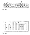
- the device shown in FIG. 3 comprises first and second transistors 40 and 42.
- the transistor 40 has an emitter 34, an active base 18b, a base contact zone 18c, an active collector 18a, a subcollector 8 and a collector contact region 20, while the transistor 42 has an emitter 36, an active base 24b, base contact zones 24c, an active collector (epitaxial zone 24a plus subcollector 6) and a collector contact region 10, 22.
- the subcollector 8 of the transistor 40 is not considered to be part of the active collector of that transistor because its high impurity concentration prevents it from being depleted of charge carriers.
- the first transistor 40 has a relatively low collector-to-base breakdown voltage BV CBO
- the second transistor 42 has a higher value of BV CBO .
- the increased value of BV CBO for the transistor 42 arises without the need for a thicker epitaxial layer beneath the zone 24b than the zone 18b, because the collector contact region 22 is spaced by dielectric isolation from the active region of the transistor (the emitter 36 and the zones 24a and 24b), and the current path between the base and the collector contact region traverses the lightly-doped subcollector 6.
- the subcollector 6 thus serves the purpose of the thick, lightly-doped epitaxial layer in the known high-voltage transistor.
- the heavily-doped region 14a serves as a channel stop between the regions 8 and 10, providing good isolation of the collectors of the two transistors.
- the breakdown voltage BV CBO of the transistor 42 depends on the depth of the zones 24c, the curvature of the boundaries of the zones 24c, the thickness and resistivity of the zone 24a, the lateral spacing between the zone 24c and the region 10, and the doping concentration of the region 6.
- a higher breakdown voltage can be obtained by increasing the radius of curvature of the boundaries of the zones 24c, by increasing the depth of the zones 24c.
- a higher breakdown voltage for the transistor 42 can also be obtained by reducing the thickness and the doping concentration of the zone 24a.
- the zone 24a has a thickness of 0.5-2 ⁇ m and a resistivity of 0.2-2 ⁇ -cm.
- compromises must be made, because reducing the thickness and doping concentration of the zone 24a implies that the thickness and doping concentration of the simultaneously-formed zone 18a will also be reduced, and this reduces the breakdown voltage of the transistor 40.
- the present invention is not restricted to the particular method and structure that have been described with reference to the drawings, and that variations may be made therein without departing from the scope of the invention as defined by the appended claims, and equivalents thereof.
- the invention is not restricted to NPN transistors, and is applicable to PNP transistors also.
- the invention is not restricted to the specific form of dielectric isolation between the collector contact region 22 and the active region of the transistor 42 that has been described, since other dielectric isolation techniques, such as trench and refill (See U. S. Patent No. 4,160,991, for example) and mesa isolation may be used instead.
Landscapes
- Bipolar Transistors (AREA)
- Bipolar Integrated Circuits (AREA)
Applications Claiming Priority (2)
| Application Number | Priority Date | Filing Date | Title |
|---|---|---|---|
| US77631785A | 1985-09-16 | 1985-09-16 | |
| US776317 | 2010-05-07 |
Publications (1)
| Publication Number | Publication Date |
|---|---|
| EP0215213A1 true EP0215213A1 (de) | 1987-03-25 |
Family
ID=25107052
Family Applications (1)
| Application Number | Title | Priority Date | Filing Date |
|---|---|---|---|
| EP86108988A Ceased EP0215213A1 (de) | 1985-09-16 | 1986-07-02 | Herstellungsverfahren von Hoch- und Niederspannungstransistoren unter Verwendung von epitaktischen Schichten gleichmässiger Dicke |
Country Status (2)
| Country | Link |
|---|---|
| EP (1) | EP0215213A1 (de) |
| JP (1) | JPS6265451A (de) |
Families Citing this family (1)
| Publication number | Priority date | Publication date | Assignee | Title |
|---|---|---|---|---|
| JPH03123033A (ja) * | 1989-10-05 | 1991-05-24 | Nec Yamagata Ltd | 半導体装置 |
Citations (2)
| Publication number | Priority date | Publication date | Assignee | Title |
|---|---|---|---|---|
| US3933540A (en) * | 1973-10-17 | 1976-01-20 | Hitachi, Ltd. | Method of manufacturing semiconductor device |
| FR2543740A1 (fr) * | 1983-03-28 | 1984-10-05 | Trt Telecom Radio Electr | Procede de realisation de transistors par integration monolithique en technologie isoplanar et circuits integres ainsi obtenus |
Family Cites Families (2)
| Publication number | Priority date | Publication date | Assignee | Title |
|---|---|---|---|---|
| JPS561826Y2 (de) * | 1973-08-17 | 1981-01-16 | ||
| JPS5623770A (en) * | 1979-08-06 | 1981-03-06 | Toshiba Corp | Manufacture of semiconductor device |
-
1986
- 1986-07-02 EP EP86108988A patent/EP0215213A1/de not_active Ceased
- 1986-09-09 JP JP61212510A patent/JPS6265451A/ja active Pending
Patent Citations (2)
| Publication number | Priority date | Publication date | Assignee | Title |
|---|---|---|---|---|
| US3933540A (en) * | 1973-10-17 | 1976-01-20 | Hitachi, Ltd. | Method of manufacturing semiconductor device |
| FR2543740A1 (fr) * | 1983-03-28 | 1984-10-05 | Trt Telecom Radio Electr | Procede de realisation de transistors par integration monolithique en technologie isoplanar et circuits integres ainsi obtenus |
Non-Patent Citations (3)
| Title |
|---|
| IBM TECHNICAL DISCLOSURE BULLETIN, vol. 22, no. 10, March 1980, pages 4450,4451, New York, US; B.K. AGGARWAL: "Double epitaxy thickness" * |
| JAPANES JOURNAL OF APPLIED PHYSICS, vol. 20, suppl. 20-1, 1981, pages 111-114, Tokyo, JP; I. IMAIZUMI et al.: "150 V high voltage linear IC technology" * |
| PATENTS ABSTRACTS OF JAPAN, vol. 5, no. 159 (E-77)[831], 14th October 1981; & JP-A-56 90 554 (TOKYO SHIBAURA DENKI K.K.) 22-07-1981 * |
Also Published As
| Publication number | Publication date |
|---|---|
| JPS6265451A (ja) | 1987-03-24 |
Similar Documents
| Publication | Publication Date | Title |
|---|---|---|
| US4458158A (en) | IC Including small signal and power devices | |
| US5539237A (en) | Schottky diode with guard ring | |
| US4137109A (en) | Selective diffusion and etching method for isolation of integrated logic circuit | |
| EP0405045B1 (de) | In gemischter Technologie hergestellte integrierte Schaltung mit CMOS-Strukturen und leistungsfähigen lateralen Bipolartransistoren mit erhöhter Early-Spannung und Herstellungsverfahren dafür | |
| EP0036082A1 (de) | Selbstjustierendes Verfahren zur Herstellung eines verbesserten hochqualitativen Bipolartransistors | |
| EP0001300B1 (de) | Verfahren zur Herstellung einer LOCOS Halbleitervorrichtung | |
| EP0685891A1 (de) | Integrierte Halbleiterdiode | |
| EP0290763B1 (de) | Hochleistungstransistor mit Seitenwandemitter | |
| US6670255B2 (en) | Method of fabricating lateral diodes and bipolar transistors | |
| US4260431A (en) | Method of making Schottky barrier diode by ion implantation and impurity diffusion | |
| EP0026276A1 (de) | Verfahren zur Herstellung fadenförmiger Sockeltransistoren | |
| EP0341461B1 (de) | Verfahren zur Herstellung einer bipolaren integrierten Schaltung | |
| EP0233202A1 (de) | Herstellung einer halbleitervorrichtung mit eingebettetem oxyd. | |
| US4819049A (en) | Method of fabricating high voltage and low voltage transistors using an epitaxial layer of uniform thickness | |
| US4860077A (en) | Vertical semiconductor device having a sidewall emitter | |
| EP0489262A1 (de) | Lateraler Bipolartransistor mit seitlich geführtem Basiskontakt und dessen Herstellungsverfahren | |
| EP0215213A1 (de) | Herstellungsverfahren von Hoch- und Niederspannungstransistoren unter Verwendung von epitaktischen Schichten gleichmässiger Dicke | |
| EP0376722B1 (de) | Herstellungsprozess für bipolare Sinkerstruktur | |
| US4326212A (en) | Structure and process for optimizing the characteristics of I2 L devices | |
| JPS6323335A (ja) | 半導体装置及びその製造方法 | |
| EP0718891B1 (de) | Hochleistungs-, Hochspannungs-, nicht-epitaxialer Bipolartransistor | |
| US4860082A (en) | Bipolar transistor | |
| JPH03190139A (ja) | 半導体集積回路装置 | |
| EP0562217B1 (de) | Lateraler Bipolartransistor mit niedrigem Leckstrom zum Substrat, entsprechende integrierte Schaltung und Verfahren zur Herstellung einer solchen integrierten Schaltung | |
| EP0385906B1 (de) | Verfahren zur Herstellung eines lateralen PNP Transistors |
Legal Events
| Date | Code | Title | Description |
|---|---|---|---|
| PUAI | Public reference made under article 153(3) epc to a published international application that has entered the european phase |
Free format text: ORIGINAL CODE: 0009012 |
|
| AK | Designated contracting states |
Kind code of ref document: A1 Designated state(s): DE FR GB NL |
|
| 17P | Request for examination filed |
Effective date: 19870811 |
|
| 17Q | First examination report despatched |
Effective date: 19900530 |
|
| STAA | Information on the status of an ep patent application or granted ep patent |
Free format text: STATUS: THE APPLICATION HAS BEEN REFUSED |
|
| 18R | Application refused |
Effective date: 19910831 |
|
| RIN1 | Information on inventor provided before grant (corrected) |
Inventor name: TANG, ALEX YIU-CHEONG Inventor name: JOHNSTON, ROGER E. |