EP0215298A2 - Laser semi-conducteur - Google Patents
Laser semi-conducteur Download PDFInfo
- Publication number
- EP0215298A2 EP0215298A2 EP86111185A EP86111185A EP0215298A2 EP 0215298 A2 EP0215298 A2 EP 0215298A2 EP 86111185 A EP86111185 A EP 86111185A EP 86111185 A EP86111185 A EP 86111185A EP 0215298 A2 EP0215298 A2 EP 0215298A2
- Authority
- EP
- European Patent Office
- Prior art keywords
- laser
- layer
- quantum well
- regions
- impurity
- Prior art date
- Legal status (The legal status is an assumption and is not a legal conclusion. Google has not performed a legal analysis and makes no representation as to the accuracy of the status listed.)
- Granted
Links
- 239000004065 semiconductor Substances 0.000 title claims abstract description 31
- 239000013078 crystal Substances 0.000 claims abstract description 29
- 239000012535 impurity Substances 0.000 claims abstract description 17
- 239000000758 substrate Substances 0.000 claims abstract description 10
- 239000000969 carrier Substances 0.000 claims abstract description 7
- 229910001218 Gallium arsenide Inorganic materials 0.000 claims description 6
- 238000005468 ion implantation Methods 0.000 claims description 4
- 238000009792 diffusion process Methods 0.000 claims description 3
- 229910000530 Gallium indium arsenide Inorganic materials 0.000 claims 1
- 238000002347 injection Methods 0.000 claims 1
- 239000007924 injection Substances 0.000 claims 1
- 230000010355 oscillation Effects 0.000 abstract description 19
- 238000005253 cladding Methods 0.000 abstract description 10
- 230000004888 barrier function Effects 0.000 description 14
- 150000002500 ions Chemical class 0.000 description 13
- 229910052710 silicon Inorganic materials 0.000 description 8
- 239000010703 silicon Substances 0.000 description 8
- -1 Silicon ions Chemical class 0.000 description 5
- XUIMIQQOPSSXEZ-UHFFFAOYSA-N Silicon Chemical compound [Si] XUIMIQQOPSSXEZ-UHFFFAOYSA-N 0.000 description 4
- 238000002513 implantation Methods 0.000 description 4
- PTFCDOFLOPIGGS-UHFFFAOYSA-N Zinc dication Chemical compound [Zn+2] PTFCDOFLOPIGGS-UHFFFAOYSA-N 0.000 description 3
- 229910052790 beryllium Inorganic materials 0.000 description 3
- ATBAMAFKBVZNFJ-UHFFFAOYSA-N beryllium atom Chemical compound [Be] ATBAMAFKBVZNFJ-UHFFFAOYSA-N 0.000 description 3
- 229910001423 beryllium ion Inorganic materials 0.000 description 3
- 238000000034 method Methods 0.000 description 3
- 230000005476 size effect Effects 0.000 description 3
- VYPSYNLAJGMNEJ-UHFFFAOYSA-N Silicium dioxide Chemical compound O=[Si]=O VYPSYNLAJGMNEJ-UHFFFAOYSA-N 0.000 description 2
- 238000005275 alloying Methods 0.000 description 2
- 229910052782 aluminium Inorganic materials 0.000 description 2
- 230000015572 biosynthetic process Effects 0.000 description 2
- 230000003247 decreasing effect Effects 0.000 description 2
- 238000005755 formation reaction Methods 0.000 description 2
- 230000001965 increasing effect Effects 0.000 description 2
- 238000010884 ion-beam technique Methods 0.000 description 2
- 239000000463 material Substances 0.000 description 2
- 230000005641 tunneling Effects 0.000 description 2
- GYHNNYVSQQEPJS-UHFFFAOYSA-N Gallium Chemical compound [Ga] GYHNNYVSQQEPJS-UHFFFAOYSA-N 0.000 description 1
- AZDRQVAHHNSJOQ-UHFFFAOYSA-N alumane Chemical group [AlH3] AZDRQVAHHNSJOQ-UHFFFAOYSA-N 0.000 description 1
- XAGFODPZIPBFFR-UHFFFAOYSA-N aluminium Chemical compound [Al] XAGFODPZIPBFFR-UHFFFAOYSA-N 0.000 description 1
- 238000000137 annealing Methods 0.000 description 1
- 229910052785 arsenic Inorganic materials 0.000 description 1
- RQNWIZPPADIBDY-UHFFFAOYSA-N arsenic atom Chemical compound [As] RQNWIZPPADIBDY-UHFFFAOYSA-N 0.000 description 1
- 229910052681 coesite Inorganic materials 0.000 description 1
- 239000000470 constituent Substances 0.000 description 1
- 230000000875 corresponding effect Effects 0.000 description 1
- 229910052906 cristobalite Inorganic materials 0.000 description 1
- 230000007547 defect Effects 0.000 description 1
- 230000000694 effects Effects 0.000 description 1
- 230000002708 enhancing effect Effects 0.000 description 1
- 229910052733 gallium Inorganic materials 0.000 description 1
- 239000007943 implant Substances 0.000 description 1
- 230000001939 inductive effect Effects 0.000 description 1
- 230000003993 interaction Effects 0.000 description 1
- 230000003287 optical effect Effects 0.000 description 1
- 230000003071 parasitic effect Effects 0.000 description 1
- 238000005036 potential barrier Methods 0.000 description 1
- 239000000377 silicon dioxide Substances 0.000 description 1
- 235000012239 silicon dioxide Nutrition 0.000 description 1
- 229910052682 stishovite Inorganic materials 0.000 description 1
- 229910052905 tridymite Inorganic materials 0.000 description 1
Images

Classifications
-
- H—ELECTRICITY
- H01—ELECTRIC ELEMENTS
- H01S—DEVICES USING THE PROCESS OF LIGHT AMPLIFICATION BY STIMULATED EMISSION OF RADIATION [LASER] TO AMPLIFY OR GENERATE LIGHT; DEVICES USING STIMULATED EMISSION OF ELECTROMAGNETIC RADIATION IN WAVE RANGES OTHER THAN OPTICAL
- H01S3/00—Lasers, i.e. devices using stimulated emission of electromagnetic radiation in the infrared, visible or ultraviolet wave range
-
- B—PERFORMING OPERATIONS; TRANSPORTING
- B82—NANOTECHNOLOGY
- B82Y—SPECIFIC USES OR APPLICATIONS OF NANOSTRUCTURES; MEASUREMENT OR ANALYSIS OF NANOSTRUCTURES; MANUFACTURE OR TREATMENT OF NANOSTRUCTURES
- B82Y20/00—Nanooptics, e.g. quantum optics or photonic crystals
-
- H—ELECTRICITY
- H01—ELECTRIC ELEMENTS
- H01S—DEVICES USING THE PROCESS OF LIGHT AMPLIFICATION BY STIMULATED EMISSION OF RADIATION [LASER] TO AMPLIFY OR GENERATE LIGHT; DEVICES USING STIMULATED EMISSION OF ELECTROMAGNETIC RADIATION IN WAVE RANGES OTHER THAN OPTICAL
- H01S5/00—Semiconductor lasers
- H01S5/04—Processes or apparatus for excitation, e.g. pumping, e.g. by electron beams
- H01S5/042—Electrical excitation ; Circuits therefor
- H01S5/0421—Electrical excitation ; Circuits therefor characterised by the semiconducting contacting layers
- H01S5/0422—Electrical excitation ; Circuits therefor characterised by the semiconducting contacting layers with n- and p-contacts on the same side of the active layer
- H01S5/0424—Electrical excitation ; Circuits therefor characterised by the semiconducting contacting layers with n- and p-contacts on the same side of the active layer lateral current injection
-
- H—ELECTRICITY
- H01—ELECTRIC ELEMENTS
- H01S—DEVICES USING THE PROCESS OF LIGHT AMPLIFICATION BY STIMULATED EMISSION OF RADIATION [LASER] TO AMPLIFY OR GENERATE LIGHT; DEVICES USING STIMULATED EMISSION OF ELECTROMAGNETIC RADIATION IN WAVE RANGES OTHER THAN OPTICAL
- H01S5/00—Semiconductor lasers
- H01S5/20—Structure or shape of the semiconductor body to guide the optical wave ; Confining structures perpendicular to the optical axis, e.g. index or gain guiding, stripe geometry, broad area lasers, gain tailoring, transverse or lateral reflectors, special cladding structures, MQW barrier reflection layers
-
- H—ELECTRICITY
- H01—ELECTRIC ELEMENTS
- H01S—DEVICES USING THE PROCESS OF LIGHT AMPLIFICATION BY STIMULATED EMISSION OF RADIATION [LASER] TO AMPLIFY OR GENERATE LIGHT; DEVICES USING STIMULATED EMISSION OF ELECTROMAGNETIC RADIATION IN WAVE RANGES OTHER THAN OPTICAL
- H01S5/00—Semiconductor lasers
- H01S5/02—Structural details or components not essential to laser action
- H01S5/0206—Substrates, e.g. growth, shape, material, removal or bonding
- H01S5/0208—Semi-insulating substrates
-
- H—ELECTRICITY
- H01—ELECTRIC ELEMENTS
- H01S—DEVICES USING THE PROCESS OF LIGHT AMPLIFICATION BY STIMULATED EMISSION OF RADIATION [LASER] TO AMPLIFY OR GENERATE LIGHT; DEVICES USING STIMULATED EMISSION OF ELECTROMAGNETIC RADIATION IN WAVE RANGES OTHER THAN OPTICAL
- H01S5/00—Semiconductor lasers
- H01S5/20—Structure or shape of the semiconductor body to guide the optical wave ; Confining structures perpendicular to the optical axis, e.g. index or gain guiding, stripe geometry, broad area lasers, gain tailoring, transverse or lateral reflectors, special cladding structures, MQW barrier reflection layers
- H01S5/2054—Methods of obtaining the confinement
- H01S5/2059—Methods of obtaining the confinement by means of particular conductivity zones, e.g. obtained by particle bombardment or diffusion
-
- H—ELECTRICITY
- H01—ELECTRIC ELEMENTS
- H01S—DEVICES USING THE PROCESS OF LIGHT AMPLIFICATION BY STIMULATED EMISSION OF RADIATION [LASER] TO AMPLIFY OR GENERATE LIGHT; DEVICES USING STIMULATED EMISSION OF ELECTROMAGNETIC RADIATION IN WAVE RANGES OTHER THAN OPTICAL
- H01S5/00—Semiconductor lasers
- H01S5/30—Structure or shape of the active region; Materials used for the active region
- H01S5/34—Structure or shape of the active region; Materials used for the active region comprising quantum well or superlattice structures, e.g. single quantum well [SQW] lasers, multiple quantum well [MQW] lasers or graded index separate confinement heterostructure [GRINSCH] lasers
- H01S5/343—Structure or shape of the active region; Materials used for the active region comprising quantum well or superlattice structures, e.g. single quantum well [SQW] lasers, multiple quantum well [MQW] lasers or graded index separate confinement heterostructure [GRINSCH] lasers in AIIIBV compounds, e.g. AlGaAs-laser, InP-based laser
- H01S5/34313—Structure or shape of the active region; Materials used for the active region comprising quantum well or superlattice structures, e.g. single quantum well [SQW] lasers, multiple quantum well [MQW] lasers or graded index separate confinement heterostructure [GRINSCH] lasers in AIIIBV compounds, e.g. AlGaAs-laser, InP-based laser with a well layer having only As as V-compound, e.g. AlGaAs, InGaAs
- H01S5/3432—Structure or shape of the active region; Materials used for the active region comprising quantum well or superlattice structures, e.g. single quantum well [SQW] lasers, multiple quantum well [MQW] lasers or graded index separate confinement heterostructure [GRINSCH] lasers in AIIIBV compounds, e.g. AlGaAs-laser, InP-based laser with a well layer having only As as V-compound, e.g. AlGaAs, InGaAs the whole junction comprising only (AI)GaAs
Definitions
- the present invention relates to a semiconductor laser capable of modulating laser oscillation at a frequency of l0 GHz or more.
- a semiconductor laser according to the present invention has a current confinement structure, which can result in comfinement of light-emitting region and hence an optical mode confinement structure for enhancing a single mode oscillation by the confinement of light-emitting region, without increasing the electric capacitance of a laser element.
- a semiconductor laser according to the present invention uses a multi quantum well layer which is larger in the height and the width of the quantum barrier compared to the conventional case wherein carriers are injected perpendicularly across the barrier layer and shows a remarkable quantum size effect, as a laser active layer, to increase the carrier density in a laser active region and to generate laser oscillation efficiently. If carriers should be injected by tunneling through the barrier layer or layers, the height and the width of the potential barrier cannot be made too large. Then, the quantum size effect due to confinement in a narrow well cannot be made large.
- the inventive parallel arrangement solves these problems.
- the capacitance of a laser element can be reduced to a least value by disposing the n+ and p+ regions at the ends of a super lattice, and thus the modulation frequency of the laser can be increased in a large degree.
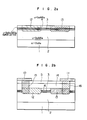
- an undoped Ga 0.5 Al 0.5 As layer 2 (having a thickness of 2 ⁇ m and serving as a cladding layer), an undoped super lattice layer 3 (serving as a laser active layer), an undoped Ga 0.5 Al 0.5 As layer 4 (having a thickness of 2 ⁇ m and serving as another cladding layer), and an undoped GaAs layer 5 (having a thickness of 0.2 ⁇ m and serving as a cap layer) are grown by the molecular beam epitaxial growth method, to form a laser structure on a semi-insulative GaAs substrate l.
- the cladding layers 2 and 4 clad the active layer 3 for generating laser oscillation, and the cap layer 5 encapsulates these structures.
- the term "undoped layer" which is herein used includes an unintentionally doped layer.
- the super lattice layer 3 is formed of GaAs layers each having a thickness of 5 nm and AlAs layers each having a thickness of 5 nm, stacked alternately. Silicon ions are accelerated by an implantation voltage of 2.3 MV and then implanted from the first open area of a mask into the laser crystal at a dose rate of 2 ⁇ l013 cm ⁇ 2 so that an n type region 6 has a silicon concentration of more than l ⁇ l018 cm ⁇ 3.
- aluminum ions are accelerated by an implantation voltage of 2.3 MV, and then implanted from the second open area of the mask into the laser crystal at a dose rate of 4 ⁇ l013 cm ⁇ 2 so that an ion implanted region 7 is formed.
- beryllium ions are accelerated by an implantation voltage of 250 KV, and then implanted from the second open area of the mask into the laser crystal, to implant the p type region 7 with beryllium.
- the ions implanted with high energies will produce a buried doped region below the surfae and that implanted impurity in the superlattice not only serves to afford conductivity but may also serve to induce alloying of the superlattice.
- Aluminum is used mainly for inducing alloying.
- silicon ions and beryllium ions are implanted into the laser crystal so as to form a silicon implanted region 8 and a beryllium implanted region 9, which serve as n-type and p-type contact regions for electrodes, respectively.
- ion implantation is carried out several times in such a manner that the implantation voltage is successively decreased, in order for the regions 8 and 9 to become an n+-type region having a uniform silicon concentration and a p+-type region having a uniform beryllium concentration.
- the laser crystal is annealed at 850°C for five hours in the atmosphere of arsenic, to convert those implanted regions of the super lattice layer 3 which are included in the implanted regions 6 and 7, into a mixed crystal by the impurity induced intermixing of gallium and aluminum atoms.
- thin potential well layers connect the p+ and n+ mixed crystal regions.
- the distance between the first and second open areas of the mask is so selected as to put the width of that region of the super lattice layer 3 which is sandwiched between the mixed crystal regions 6 and 7, in a range from 0.8 to l.5 ⁇ m.
- a super lattice multi-quantum-well
- impurity atoms When a super lattice (multi-quantum-well) includes impurity atoms and is applied with thermal energy of certain order, intermixing of constituent atoms occur among all the barrier and well layers to form a mixed crystal, i.e. vanish MQW.
- the required impurity atoms may be implanted or diffused. The resultant region will have a low resistivity.
- a negative electrode l0 and a positive electrode ll is provided on the same surface of the laser crystal in the form of a stripe having a width of l0 ⁇ m.
- Each electrode has a outwardly protruding pad for bonding, at a central portion thereof.
- the length of a laser cavity is made equal to l50 ⁇ m.
- the above semiconductor laser had an electric capacitance of less than l pF, and the threshold current of laser oscillation was 5 mA. Further, in the room temperature operation generating an output of 5 mW, an output drop of 3 dB was observed at a modulation frequency of l7 GHz. In the case of the l0-mW output, an output drop of 3 dB was observed at a modulation frequency of 23 GHz.
- the present embodiment can modulate laser oscillation at such a high frequency.
- it is not required to inject carriers into the super lattice layer in directions perpendicular thereto, i.e. across the barrier layer.
- the barrier outside a quantum well can be made sufficiently large in height by selecting an appropriate material for the barrier layer, and thus the overflow loss of carriers can be reduced.
- the width of the barrier layer on both sides of a well layer can be made sufficiently wide, and thus the energy state broadening at individual quantum wells by sub-band formation can be prevented. Accordingly, a variation in the amount of injected carriers causes a large change in gain, and hence the present embodiment is high in relaxation oscillation frequency f r .
- the present embodiment can modulate laser oscillation at a high frequency.
- a pn junction is formed in such a manner that the super lattice region having a width of about l ⁇ m is sandwiched between the n-type ion-implanted region 6 and the p-type ion-implanted region 7, each of which has a thickness of thousands of angstroms. Accordingly, the pn junction is far smaller in junction capacitance than the pn junction of an ordinary semiconductor laser.
- the electric resistance between the p-type region 7 and the n-type region 6 is reduced, and thus the capacitance between the ion-implanted regions 6 and 8 and the ion-implanted regions 7 and 9, are as if they are shunted by a low-resistance current path, because the super lattice layer 3 therebetween has a low resistivity. That is, the above capacitance has only a little effect on a modulating operation.
- impurity doping is carried out only by ion implation.
- the present embodiment can modulate laser oscillation at a very high frequency.
- impurity diffusion can be employed as well, e.g. for the formation of the regions 8 and 9. When diffusion is employed, annealing is not always necessary.
- FIG. 2a Another embodiment of a semiconductor laser according to the present invention is formed by using an ion implantor, a molecular beam epitaxial growth apparatus, and an ultra-high vacuum transport chamber disposed between the ion implantor and the molecular beam epitaxial growth apparatus.
- an undoped Ga 0.5 Al 0.5 As layer 2 serving as a cladding layer
- an undoped super lattice layer 3 serving as a laser active layer
- an undoped Ga 0.5 Al 0.5 As layer 4 serving as another cladding layer
- the super lattice layer 3 is formed of Ga 0.9 Al 0.l As layers each having a thicknes of 6 nm and AlAs layers each having a thickness of 8 nm.
- the semiconductor crystal and the substrate are transferred to the ion implantor through the transport chamber, and then silicon ions are implanted into a region l2 through the maskless ion implantation technique using a silicon ion beam.
- zinc ions are implanted into a region l3 by a zinc ion beam.
- the thickness of the cladding layer 4 is made small (for example, equal to 50 nm) so that zinc ions can reach the super lattice layer 3.
- the semiconductor crystal and the substrate are returned to the molecular beam epitaxial growth apparatus through the transport chamber.
- an undoped Ga 0.5 Al 0.5 As layer l4 (serving as an extended portion of the cladding layer 4) and an undoped GaAs layer 5 (serving as a cap layer) are successively grown.
- a laser structure thus obtained is transferred to the ion implantor through the transport chamber, and then silicon ions and beryllium ions are implanted into regions l5 and l6, respectively. Thereafter, the crystal is annealed at 750°C, to activate implanted ions and to convert those regions of the super lattice layer 3 which are included in the ion implanted regions l2 and l3, into a mixed crystal, thereby obtaining the buried heterostructure of super lattice.
- electrodes l0 and ll are formed so as to be put in ohmic contact with the ion implanted regions l5 and l6, respectively.
- the present embodiment having a cavity length of l50 ⁇ m was attached to a high-frequency mount, to study the modulation characteristics of the embodiment. According to the inventor's experiments, in the room temperature operation generating an output of 5 mW, an output drop of 3 dB was observed at a modulation frequency of 20 GHz. In the case of the l0-mW output, an output drop of 3 dB was observed at a modulation frequency of 25 GHz.
- a further embodiment of a semiconductor laser according to the present invention is fabricated in the following manner.
- An undoped InP layer (having a thickness of 2 ⁇ m and serving as a cladding layer), an undoped Al 0.52 In 0.48 As layer (having a thickness of 0.5 ⁇ m and serving as a barrier layer), an undoped multi quantum well layer (having a thickness of 0.5 ⁇ m and serving as a laser active layer), an undoped Al 0.52 In 0.48 As layer (having a thickness of 0.5 ⁇ m and serving as another barrier layer), an undoped InP layer (having a thickness of l.5 ⁇ m and serving as another cladding layer), and an undoped Ga 0.47 In 0.53 As layer (having a thickness of 0.l ⁇ m and serving as a cap layer) are grown in this order by the molecular beam epitaxial growth method using gas sources, to form a laser structure on a semi-insulative InP substrate.
- the multi quantum well layer is formed in such a manner that a Ga 0.47 In 0.53 As layer (having a thickness of l0 nm and serving as a quantum well layer) and an Al 0.52 In 0.48 As layer (having a thickness of l0 nm and serving as a barrier layer) are alternately and repeatedly grown.
- the structure thus obtained is subjected to the same processing as described in the EMBODIMENT I. That is, the laser structure is implanted with impurity ions and is then annealed so that the ion implanted region of the multi quantum well layer (namely, the super lattice layer) is converted into a mixed crystal layer and ion implanted regions make up such a current path as shown in Fig. l.
- the above embodiment generated laser oscillation having a single transverse mode, had an oscillation wavelength of l.52 ⁇ m, and was able to modulate laser oscillation at a very high frequency. That is, the modulation frequency corresponding to an output drop of 3 dB was l6 GHz.
- the thickness of each of quantum well layers included in the multi quantum well layer lies in a range from 3 to 20 nm and the thickness of each of barrier layers included in the multi quantum well layer lies in a range from 2 to 40 nm.
- the thickness of each quantum well layer and that of each barrier layer are made too small to lie below the respective ranges, a mutual interaction will abruptly increase between quantum wells, and thus the function of quantum well is lost.
- the thickness of each quantum well layer and that of each barrier layer are made so large as to exceed the respective upper limits. The quantum size effect of the quantum well layer is alruptly decreased, and thus it becomes impossible to modulate laser oscillation at a very high frequency and to control the mode of laser oscillation.
- the total thickness of the multi quantum well layer in a range from 0.0l to 0.l5 ⁇ m.
Landscapes
- Physics & Mathematics (AREA)
- Optics & Photonics (AREA)
- Electromagnetism (AREA)
- Engineering & Computer Science (AREA)
- Condensed Matter Physics & Semiconductors (AREA)
- General Physics & Mathematics (AREA)
- Nanotechnology (AREA)
- Chemical & Material Sciences (AREA)
- Biophysics (AREA)
- Crystallography & Structural Chemistry (AREA)
- Life Sciences & Earth Sciences (AREA)
- Geometry (AREA)
- Plasma & Fusion (AREA)
- Semiconductor Lasers (AREA)
Applications Claiming Priority (2)
| Application Number | Priority Date | Filing Date | Title |
|---|---|---|---|
| JP60206444A JPS6267890A (ja) | 1985-09-20 | 1985-09-20 | 半導体レ−ザ |
| JP206444/85 | 1985-09-20 |
Publications (3)
| Publication Number | Publication Date |
|---|---|
| EP0215298A2 true EP0215298A2 (fr) | 1987-03-25 |
| EP0215298A3 EP0215298A3 (en) | 1990-01-24 |
| EP0215298B1 EP0215298B1 (fr) | 1992-11-11 |
Family
ID=16523474
Family Applications (1)
| Application Number | Title | Priority Date | Filing Date |
|---|---|---|---|
| EP86111185A Expired - Lifetime EP0215298B1 (fr) | 1985-09-20 | 1986-08-12 | Laser semi-conducteur |
Country Status (5)
| Country | Link |
|---|---|
| US (1) | US4752934A (fr) |
| EP (1) | EP0215298B1 (fr) |
| JP (1) | JPS6267890A (fr) |
| KR (1) | KR900000022B1 (fr) |
| DE (1) | DE3687102T2 (fr) |
Cited By (9)
| Publication number | Priority date | Publication date | Assignee | Title |
|---|---|---|---|---|
| GB2200248A (en) * | 1986-12-15 | 1988-07-27 | Sharp Kk | A semiconductor laser device |
| US4852111A (en) * | 1986-12-15 | 1989-07-25 | 501 Sharp Kabushiki Kaisha | Semiconductor laser device |
| US4860299A (en) * | 1987-05-19 | 1989-08-22 | Sharp Kabushiki Kaisha | Semiconductor laser device |
| US4862470A (en) * | 1987-04-28 | 1989-08-29 | Sharp Kabushiki Kaisha | Semiconductor laser device |
| US4862472A (en) * | 1987-01-16 | 1989-08-29 | Sharp Kabushiki Kaisha | Semiconductor laser device |
| US4868838A (en) * | 1986-07-10 | 1989-09-19 | Sharp Kabushiki Kaisha | Semiconductor laser device |
| US4894836A (en) * | 1987-02-24 | 1990-01-16 | Sharp Kabushiki Kaisha | Semiconductor device |
| US4910744A (en) * | 1986-12-09 | 1990-03-20 | Sharp Kabushiki Kaisha | Buried heterostructure semiconductor laser device |
| EP0293000A3 (en) * | 1987-05-29 | 1990-08-08 | Hitachi, Ltd. | Light emitting device |
Families Citing this family (13)
| Publication number | Priority date | Publication date | Assignee | Title |
|---|---|---|---|---|
| US4786951A (en) * | 1985-02-12 | 1988-11-22 | Mitsubishi Denki Kabushiki Kaisha | Semiconductor optical element and a process for producing the same |
| JPH0775265B2 (ja) * | 1988-02-02 | 1995-08-09 | 三菱電機株式会社 | 半導体レーザおよびその製造方法 |
| US4987468A (en) * | 1988-06-17 | 1991-01-22 | Xerox Corporation | Lateral heterojunction bipolar transistor (LHBT) and suitability thereof as a hetero transverse junction (HTJ) laser |
| US5164797A (en) * | 1988-06-17 | 1992-11-17 | Xerox Corporation | Lateral heterojunction bipolar transistor (LHBT) and suitability thereof as a hetero transverse junction (HTJ) laser |
| US4873696A (en) * | 1988-10-31 | 1989-10-10 | The Regents Of The University Of California | Surface-emitting lasers with periodic gain and a parallel driven nipi structure |
| JPH0777278B2 (ja) * | 1988-12-09 | 1995-08-16 | 三菱電機株式会社 | 半導体レーザおよびその製造方法 |
| JPH02196486A (ja) * | 1989-01-24 | 1990-08-03 | Mitsubishi Electric Corp | 半導体レーザの製造方法 |
| US5063569A (en) * | 1990-12-19 | 1991-11-05 | At&T Bell Laboratories | Vertical-cavity surface-emitting laser with non-epitaxial multilayered dielectric reflectors located on both surfaces |
| JPH04291304A (ja) * | 1991-03-20 | 1992-10-15 | Fujitsu Ltd | 光導波路および光信号の制御方法 |
| US5406574A (en) * | 1991-10-23 | 1995-04-11 | Kabushiki Kaisha Toshiba | Semiconductor laser device |
| JP2677232B2 (ja) * | 1995-02-23 | 1997-11-17 | 日本電気株式会社 | 長波長半導体レーザおよびその製造方法 |
| US5661740A (en) * | 1996-04-16 | 1997-08-26 | The United States Of America As Represented By The Secretary Of The Army | TEM mode quantum wire or well structure |
| US6369403B1 (en) * | 1999-05-27 | 2002-04-09 | The Board Of Trustees Of The University Of Illinois | Semiconductor devices and methods with tunnel contact hole sources and non-continuous barrier layer |
Family Cites Families (8)
| Publication number | Priority date | Publication date | Assignee | Title |
|---|---|---|---|---|
| JPS5511371A (en) * | 1978-07-10 | 1980-01-26 | Mitsubishi Electric Corp | Semiconductor laser system |
| US4511408A (en) * | 1982-04-22 | 1985-04-16 | The Board Of Trustees Of The University Of Illinois | Semiconductor device fabrication with disordering elements introduced into active region |
| US4594603A (en) * | 1982-04-22 | 1986-06-10 | Board Of Trustees Of The University Of Illinois | Semiconductor device with disordered active region |
| JPS58225680A (ja) * | 1982-06-23 | 1983-12-27 | Nec Corp | 半導体レ−ザ |
| JPS5944797B2 (ja) * | 1982-07-28 | 1984-11-01 | 工業技術院長 | 半導体レ−ザ装置の製造方法 |
| JPS5923584A (ja) * | 1982-07-29 | 1984-02-07 | Nec Corp | 半導体レ−ザ |
| JPS607789A (ja) * | 1983-06-28 | 1985-01-16 | Agency Of Ind Science & Technol | プレ−ナ型半導体発光装置 |
| NL8304008A (nl) * | 1983-11-22 | 1985-06-17 | Philips Nv | Halfgeleiderinrichting voor het opwekken van elektro-magnetische straling. |
-
1985
- 1985-09-20 JP JP60206444A patent/JPS6267890A/ja active Pending
-
1986
- 1986-07-28 KR KR1019860006144A patent/KR900000022B1/ko not_active Expired
- 1986-08-12 DE DE8686111185T patent/DE3687102T2/de not_active Expired - Fee Related
- 1986-08-12 EP EP86111185A patent/EP0215298B1/fr not_active Expired - Lifetime
- 1986-08-20 US US06/898,199 patent/US4752934A/en not_active Expired - Fee Related
Cited By (12)
| Publication number | Priority date | Publication date | Assignee | Title |
|---|---|---|---|---|
| US4868838A (en) * | 1986-07-10 | 1989-09-19 | Sharp Kabushiki Kaisha | Semiconductor laser device |
| US4910744A (en) * | 1986-12-09 | 1990-03-20 | Sharp Kabushiki Kaisha | Buried heterostructure semiconductor laser device |
| GB2200248A (en) * | 1986-12-15 | 1988-07-27 | Sharp Kk | A semiconductor laser device |
| US4852111A (en) * | 1986-12-15 | 1989-07-25 | 501 Sharp Kabushiki Kaisha | Semiconductor laser device |
| US4887274A (en) * | 1986-12-15 | 1989-12-12 | Sharp Kabushiki Kaisha | Deterioration-resistant superlattice semiconductor laser device |
| US4907239A (en) * | 1986-12-15 | 1990-03-06 | Sharp Kabushiki Kaisha | Semiconductor laser device |
| GB2200248B (en) * | 1986-12-15 | 1991-03-20 | Sharp Kk | A semiconductor laser device |
| US4862472A (en) * | 1987-01-16 | 1989-08-29 | Sharp Kabushiki Kaisha | Semiconductor laser device |
| US4894836A (en) * | 1987-02-24 | 1990-01-16 | Sharp Kabushiki Kaisha | Semiconductor device |
| US4862470A (en) * | 1987-04-28 | 1989-08-29 | Sharp Kabushiki Kaisha | Semiconductor laser device |
| US4860299A (en) * | 1987-05-19 | 1989-08-22 | Sharp Kabushiki Kaisha | Semiconductor laser device |
| EP0293000A3 (en) * | 1987-05-29 | 1990-08-08 | Hitachi, Ltd. | Light emitting device |
Also Published As
| Publication number | Publication date |
|---|---|
| EP0215298A3 (en) | 1990-01-24 |
| DE3687102D1 (de) | 1992-12-17 |
| US4752934A (en) | 1988-06-21 |
| KR900000022B1 (ko) | 1990-01-18 |
| KR870003593A (ko) | 1987-04-18 |
| DE3687102T2 (de) | 1993-03-25 |
| JPS6267890A (ja) | 1987-03-27 |
| EP0215298B1 (fr) | 1992-11-11 |
Similar Documents
| Publication | Publication Date | Title |
|---|---|---|
| EP0215298B1 (fr) | Laser semi-conducteur | |
| Maranowski et al. | Native oxide top‐and bottom‐confined narrow stripe p‐n Al y Ga1− y As‐GaAs‐In x Ga1− x As quantum well heterostructure laser | |
| US5202896A (en) | Bipolar inversion channel field effect transistor laser | |
| US5028563A (en) | Method for making low tuning rate single mode PbTe/PbEuSeTe buried heterostructure tunable diode lasers and arrays | |
| EP0210616B1 (fr) | Laser à semi-conducteur | |
| Deppe et al. | Low‐threshold disorder‐defined buried‐heterostructure Al x Ga1− x As‐GaAs quantum well lasers | |
| US6751243B2 (en) | Semiconductor device with quantum dots having high carrier injection efficiency, its manufacture method, and semiconductor laser device | |
| US4937835A (en) | Semiconductor laser device and a method of producing same | |
| EP0400559A2 (fr) | Dispositif optique à semi-conducteur | |
| JPH06104533A (ja) | 青色発光素子およびその製造方法 | |
| US4881235A (en) | Semiconductor laser having a multiple quantum well structure doped with impurities | |
| EP0530942B1 (fr) | Dispositif de commutation opto-électronique à puits quantiques à émission stimulée | |
| GB2252872A (en) | Laser diode and method of manufacture | |
| US4959696A (en) | Three terminal tunneling device and method | |
| US5422902A (en) | BeTe-ZnSe graded band gap ohmic contact to p-type ZnSe semiconductors | |
| US4933728A (en) | Semiconductor optical device | |
| US5107306A (en) | Semiconductor device having a waveguide structure | |
| US7023896B2 (en) | VCSEL structure insensitive to mobile hydrogen | |
| JP3604400B2 (ja) | 半導体レーザ素子 | |
| JPH01198088A (ja) | 半導体レーザおよびその製造方法 | |
| US4943971A (en) | Low tuning rate single mode PbTe/PbEuSeTe buried heterostructure tunable diode lasers and arrays | |
| JPH02121382A (ja) | 埋込みストライプ半導体レーザーの製造方法及びその半導体レーザー | |
| US5119388A (en) | Low tuning rate PbTe/PbEuSeTe buried quantum well tunable diode lasers and arrays | |
| JPH065920A (ja) | 発光素子 | |
| US5567646A (en) | Method of making a stripe-geometry II/VI semiconductor gain-guided injection laser structure using ion implantation |
Legal Events
| Date | Code | Title | Description |
|---|---|---|---|
| PUAI | Public reference made under article 153(3) epc to a published international application that has entered the european phase |
Free format text: ORIGINAL CODE: 0009012 |
|
| AK | Designated contracting states |
Kind code of ref document: A2 Designated state(s): DE FR GB |
|
| PUAL | Search report despatched |
Free format text: ORIGINAL CODE: 0009013 |
|
| AK | Designated contracting states |
Kind code of ref document: A3 Designated state(s): DE FR GB |
|
| 17P | Request for examination filed |
Effective date: 19900629 |
|
| 17Q | First examination report despatched |
Effective date: 19910809 |
|
| GRAA | (expected) grant |
Free format text: ORIGINAL CODE: 0009210 |
|
| AK | Designated contracting states |
Kind code of ref document: B1 Designated state(s): DE FR GB |
|
| REF | Corresponds to: |
Ref document number: 3687102 Country of ref document: DE Date of ref document: 19921217 |
|
| ET | Fr: translation filed | ||
| PLBE | No opposition filed within time limit |
Free format text: ORIGINAL CODE: 0009261 |
|
| STAA | Information on the status of an ep patent application or granted ep patent |
Free format text: STATUS: NO OPPOSITION FILED WITHIN TIME LIMIT |
|
| 26N | No opposition filed | ||
| PGFP | Annual fee paid to national office [announced via postgrant information from national office to epo] |
Ref country code: FR Payment date: 19940621 Year of fee payment: 9 |
|
| PGFP | Annual fee paid to national office [announced via postgrant information from national office to epo] |
Ref country code: GB Payment date: 19940802 Year of fee payment: 9 |
|
| PGFP | Annual fee paid to national office [announced via postgrant information from national office to epo] |
Ref country code: DE Payment date: 19941027 Year of fee payment: 9 |
|
| PG25 | Lapsed in a contracting state [announced via postgrant information from national office to epo] |
Ref country code: GB Effective date: 19950812 |
|
| GBPC | Gb: european patent ceased through non-payment of renewal fee |
Effective date: 19950812 |
|
| PG25 | Lapsed in a contracting state [announced via postgrant information from national office to epo] |
Ref country code: FR Effective date: 19960430 |
|
| PG25 | Lapsed in a contracting state [announced via postgrant information from national office to epo] |
Ref country code: DE Effective date: 19960501 |
|
| REG | Reference to a national code |
Ref country code: FR Ref legal event code: ST |