EP0215436A2 - Méthode de croissance d'une couche mince pour semi-conducteur composite - Google Patents
Méthode de croissance d'une couche mince pour semi-conducteur composite Download PDFInfo
- Publication number
- EP0215436A2 EP0215436A2 EP86112487A EP86112487A EP0215436A2 EP 0215436 A2 EP0215436 A2 EP 0215436A2 EP 86112487 A EP86112487 A EP 86112487A EP 86112487 A EP86112487 A EP 86112487A EP 0215436 A2 EP0215436 A2 EP 0215436A2
- Authority
- EP
- European Patent Office
- Prior art keywords
- substrate
- layer
- composite semiconductor
- molecular beam
- temperature
- Prior art date
- Legal status (The legal status is an assumption and is not a legal conclusion. Google has not performed a legal analysis and makes no representation as to the accuracy of the status listed.)
- Granted
Links
Images


Classifications
-
- C—CHEMISTRY; METALLURGY
- C30—CRYSTAL GROWTH
- C30B—SINGLE-CRYSTAL GROWTH; UNIDIRECTIONAL SOLIDIFICATION OF EUTECTIC MATERIAL OR UNIDIRECTIONAL DEMIXING OF EUTECTOID MATERIAL; REFINING BY ZONE-MELTING OF MATERIAL; PRODUCTION OF A HOMOGENEOUS POLYCRYSTALLINE MATERIAL WITH DEFINED STRUCTURE; SINGLE CRYSTALS OR HOMOGENEOUS POLYCRYSTALLINE MATERIAL WITH DEFINED STRUCTURE; AFTER-TREATMENT OF SINGLE CRYSTALS OR A HOMOGENEOUS POLYCRYSTALLINE MATERIAL WITH DEFINED STRUCTURE; APPARATUS THEREFOR
- C30B29/00—Single crystals or homogeneous polycrystalline material with defined structure characterised by the material or by their shape
- C30B29/10—Inorganic compounds or compositions
- C30B29/40—AIIIBV compounds wherein A is B, Al, Ga, In or Tl and B is N, P, As, Sb or Bi
-
- C—CHEMISTRY; METALLURGY
- C30—CRYSTAL GROWTH
- C30B—SINGLE-CRYSTAL GROWTH; UNIDIRECTIONAL SOLIDIFICATION OF EUTECTIC MATERIAL OR UNIDIRECTIONAL DEMIXING OF EUTECTOID MATERIAL; REFINING BY ZONE-MELTING OF MATERIAL; PRODUCTION OF A HOMOGENEOUS POLYCRYSTALLINE MATERIAL WITH DEFINED STRUCTURE; SINGLE CRYSTALS OR HOMOGENEOUS POLYCRYSTALLINE MATERIAL WITH DEFINED STRUCTURE; AFTER-TREATMENT OF SINGLE CRYSTALS OR A HOMOGENEOUS POLYCRYSTALLINE MATERIAL WITH DEFINED STRUCTURE; APPARATUS THEREFOR
- C30B23/00—Single-crystal growth by condensing evaporated or sublimed materials
- C30B23/02—Epitaxial-layer growth
-
- H—ELECTRICITY
- H10—SEMICONDUCTOR DEVICES; ELECTRIC SOLID-STATE DEVICES NOT OTHERWISE PROVIDED FOR
- H10P—GENERIC PROCESSES OR APPARATUS FOR THE MANUFACTURE OR TREATMENT OF DEVICES COVERED BY CLASS H10
- H10P14/00—Formation of materials, e.g. in the shape of layers or pillars
- H10P14/20—Formation of materials, e.g. in the shape of layers or pillars of semiconductor materials
- H10P14/22—Formation of materials, e.g. in the shape of layers or pillars of semiconductor materials using physical deposition, e.g. vacuum deposition or sputtering
-
- H—ELECTRICITY
- H10—SEMICONDUCTOR DEVICES; ELECTRIC SOLID-STATE DEVICES NOT OTHERWISE PROVIDED FOR
- H10P—GENERIC PROCESSES OR APPARATUS FOR THE MANUFACTURE OR TREATMENT OF DEVICES COVERED BY CLASS H10
- H10P14/00—Formation of materials, e.g. in the shape of layers or pillars
- H10P14/20—Formation of materials, e.g. in the shape of layers or pillars of semiconductor materials
- H10P14/29—Formation of materials, e.g. in the shape of layers or pillars of semiconductor materials characterised by the substrates
- H10P14/2901—Materials
- H10P14/2907—Materials being Group IIIA-VA materials
- H10P14/2909—Phosphides
-
- H—ELECTRICITY
- H10—SEMICONDUCTOR DEVICES; ELECTRIC SOLID-STATE DEVICES NOT OTHERWISE PROVIDED FOR
- H10P—GENERIC PROCESSES OR APPARATUS FOR THE MANUFACTURE OR TREATMENT OF DEVICES COVERED BY CLASS H10
- H10P14/00—Formation of materials, e.g. in the shape of layers or pillars
- H10P14/20—Formation of materials, e.g. in the shape of layers or pillars of semiconductor materials
- H10P14/32—Formation of materials, e.g. in the shape of layers or pillars of semiconductor materials characterised by intermediate layers between substrates and deposited layers
- H10P14/3202—Materials thereof
- H10P14/3214—Materials thereof being Group IIIA-VA semiconductors
- H10P14/3221—Arsenides
-
- H—ELECTRICITY
- H10—SEMICONDUCTOR DEVICES; ELECTRIC SOLID-STATE DEVICES NOT OTHERWISE PROVIDED FOR
- H10P—GENERIC PROCESSES OR APPARATUS FOR THE MANUFACTURE OR TREATMENT OF DEVICES COVERED BY CLASS H10
- H10P14/00—Formation of materials, e.g. in the shape of layers or pillars
- H10P14/20—Formation of materials, e.g. in the shape of layers or pillars of semiconductor materials
- H10P14/34—Deposited materials, e.g. layers
- H10P14/3402—Deposited materials, e.g. layers characterised by the chemical composition
- H10P14/3414—Deposited materials, e.g. layers characterised by the chemical composition being group IIIA-VIA materials
- H10P14/3421—Arsenides
Definitions
- the present invention relates to a method of growth of a thin film for use in a composite semiconductor, and more particularly to a method of growing crystal for providing composite semiconductor thin films for use in microwave elements, photo emissive elements and/or photo receiving elements.
- HEMT high electron mobility transistor
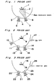
- FIGs. 1,.2 and 3 are schematic diagrams showing top plan view of an apparatus for the process of a so called molecular epitaxial growing (referred to as MBE method) in the conventional III-V composite semiconductor.
- Fig. 1 denotes a holder for holding a substrate 2
- 3 denotes a cell shutter
- 4 denotes III group sample such as Ga or In
- 5 and 7 denote cells
- 6 denotes V group sample such as As or P.
- the V group elements are converted into atomic states or molecular states in the high vacuum growing chamber and radiated from the cell 7, whereby the substrate is heated up to a high temperature by illuminating light to the substrate 2 suppressing removal of the V group elements from the substrate 2 so that the impurities situated on the surface of the substrate are removed.
- the semiconductor chip is heated up above the critical temperature, there may occur an alloying reaction in both thin film of the lower layer and surface electrode metal, then the thin film of the lower layer is damaged.
- the lower layer is formed of multi thin layers, there occurs diffusion of the doping atoms between the two adjacent thin layers and mother atoms, thereby lowering the electronic characteristics on the interface of the thin film and the thin film per se.
- FIG. 2 Another MBE method of growing III-V group composite semiconductor thin layer is shown in Fig. 2, wherein 8 is a substrate holder, 9 is a substrate, 10 is an ion gun, 11 and 14 are cell shutters, 12 is a III group material, 13 and 16 are cells, 15 is V-group material and 17 is an entrance for Argon gas.
- Ar ion beam is projected by the ion gun 10 onto the surface of the substrate 9 by introducing the Ar gas in the vacuum device, whereby the surface of the substrate 9 is cleaned off without temperature rise.
- radiation of the Ar beam causes the surface of the substrate 9 to be remarkably optically damaged and the crystal characteristic is disturbed, whereby a lot of defaults occur. As a result the crystallization and the electronic characteristic of the surface of the top layer grown on the substrate are lowered.
- a further approach is to use so called a vapor phase epitaxial growth as the MBE method wherein there is used as shown in Fig. 3 a chemical vapor phase etching against the surface of the substrate by means of reactive gas such as HCL gas immediately before the crystal growth.
- a chemical vapor phase etching against the surface of the substrate by means of reactive gas such as HCL gas immediately before the crystal growth In Fig. 3, 18 is a substrate holder, 20 and 23 are cell shutters, 21 is a III group material, 22 and 25 are cells, 24 is V group material and 26 is an entrance to introduce the reaction gas.
- the method shown in Fig. 5 it is possible to clean the surface of the substrate without causing the substrate to be heated or damaged.
- reaction gas to introduce the reaction gas into the vacuum device causes the material forming the vacuum device and exhausting path of the vacuam device to be undesirably etched, in addition the reaction gas may reacts with fine wires such as heaters. These phenomena invite serious problems for the stable operation of the vacuum device.
- To etch the members of the device other than the substrate causes to generate impurity gas, thus the electronic characteristic of the III-V group composite semiconductor formed after the etching is lowered.
- the conventional method of making the MSL is to alternatively open and close the shatters 3 and 3'so as to grow the GaAs layer and AlAs layer alternatively periodically and to obtain a hetero interfaces.
- the hetero interfaces grown by the conventional method has a disadvantage that the surface of the hetero interface is not flat but is fluctuated with more than 1 atomic thick.
- Such fluctuation or projection and recess of the surface of the hetero interface causes the light wave length radiated from a quantum well type light emission element to be shifted and lowering the control of the characteristic of the light emission element.
- the hetero interface such as a high electron mobility transistor (HEMT)
- HEMT high electron mobility transistor
- the surface of the hetero interface is fluctuated more than 1 atomic thick it has not been made to form the MSL on over all surface of the wafer of 2 inch diameter.
- An essential object of the present invention is to provide a method of growth of a thin film layer in a composite semiconductor which enables to form the thin film layer having a desired characteristics without being effected by the state of the surface of the substrate and the lower film layer.
- Another object of the present invention is to provide a method of growth of a thin film layer formed by 1 atomic layer correctly without fluctuation of the surface of the thin layer.
- a further object of the present invention is to provide a method of manufacturing a thin film layer of the composite semiconductor in which the impurities in a ssubstrate or a lower layer of the composite semiconductor can be completely removed without causing the surface of the substrate or lower layer to be damaged by radiation of molecular beam.
- a still further object of the present invention is to provide a method of manufacturing a thin film layer of the composite semiconductor in which the high speed electron mobility can be obtained.
- a still further objeqt of the present invention is to provide a method of manufacturing a thin film layer of the composite semiconductor having only 1 atomic thick without projection and recess by an easy control of the molecular beam.
- a method of the production of a composite semiconductor which comprises, a step of removing impurity molecules on a substrate or lower layer of the composite semiconductor by projecting III group molecular beam or V group molecular beam onto a substrate or a lower layer of the composite semiconductor before growth of an epitaxial layer thereon, and a step of growing a thin film layer of III group and V group atom composite semiconductor on the substrate or the lower layer of the composite semiconductor
- the present inventor conducted various studies through Auger electron spectrophotometric analysis of the composite semiconductor substrate and the lower layer of the composite semiconductor substrate. Then the present inventor has discovered the following phenomena. For example, after thermal cleaning of an InP substrate at 400° C for 1 hour under radiation of arsenic (As) molecules of V group elements, there remain impurity atoms such as C (carbon) and 0 (oxygen) on the surface of the InP substrate.. However, in the cleaning process mentioned above,- it has been found that the Auger electron peak caused by the impurity atoms such as oxygen (0) or carbon (C) could be removed as shown in Fig.
- radiation of Sb molecular beam with the number of atoms not more than the number of atoms necessary for one atomic layer enables to remove the impurity atoms on the composite semiconductor substrate or the surface of the lower layer of the composite semiconductor below the critical temperature. Also different from method of radiation of the ion beam, radiation of the neutral atomic beam does not injure the surface of the substrate. Moreover, the method according to the present invention does not etch the vacuum device per se as occur when the reaction gas is used.
- a method of molecular epitaxial growth for growing single crystal on a substrate situated in a growing chamber by projecting material accommodated in a cell to the substrate under a high vacuum comprising a step of keeping a temperature of the substrate after the material is applied to the substrate or keep a temperature after the substrate is heated up to a predetermined temperature, a step of removing excessive atoms which are present to form more than 1 atomic layer so that 1 atomic layer is formed on the substrate, and fitting a different material on the substrate so as to form a flat layer without projection and recess.
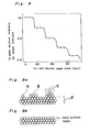
- Fig. 8 shows a result of the Auger electron spectrum analysis in the adjacent analysis chamber keeping a high vacuum with the background vacuum of 5 x 10 - 11 Torr to 1 x 10- 10 Torr without taking the InP substrate out of the vacuum device after application of Ga material onto the surface of InP substrate under As pressure of 1 x 10 -6 Torr to 1 x 10 -5 Torr at the temperature 400° C to 500 °C of the substrate.
- the vertical axis shows the relative peak value of the Auger electron intensity taking the peak intensity of the Auger electron spectro of the InP substrate as 1,0.
- the horizontal axis shows the time during which radiation of Ga material with the Ga cell shutter opened.
- the time shown in Fig. 8 corresponds to the time from the opening of the Ga cell shutter to the closure thereof.
- the time is plotted with the interval of about 4 to 5 seconds, and the plot corresponds to 20 seqonds does not mean that the radiation of the Ga material for 4 seconds is repeated four times but means the radiation for 20 seconds of one time.
- the longer the releasing time of the shutter or evaporation of Ga material the weaker the intensity of the In peak.
- the rate of detection of In Auger electron at the substrate decrease since Ga atoms are applied on the surface of the InP substrate.
- the intensity of the peak is reduced every 15 to 16 seconds abruptly. This means the following phenomenon. For example, from 0 second to 16 second, there is no variation of the peak intensity. In other words, in case Ga cell shutter is opened only for less the 16 seconds, Ga atoms once applied to the surface of InP substrate is away from the surface of the substrate while the temperature of the substrate falls below a room temperature after the Ga cell shutter is closed during 30 minutes, then the surface of the substrate appears again.
- the thickness of GaAs layer when continuous growth is performed for 3 hours with the Ga molecular intensity, As pressure and the substrate temperature are kept unchanged is about 0.19 um, therefore, the thickness of GaAs layer in case of continuous growth is 2.8 A,so that the Ga As thickness corresponds to 1 atomic thickness within the measurement error range. This phenomenon can be explained as follows.
- Fig. 9a There are formed isolated atom A and two dimensional crust B and three dimensional crust C on the outermost surface of the growth layer as shown in Fig. 9a.
- the cross sectional view at the portion near the outermost surface of the growth layer having a complete flat surface can be shown as Fig. 9b with respective to the atom layer level.
- the atoms situated on the outermost surface are conflicted by the four most adjacent atoms by the atomic bonding force.
- the isolated atom A in Fig. 9b is conflicted only by two most adjacent atoms
- the atom in the end of the two dimensional crust B is conflicted only by three most adjacent atoms.
- the atoms on the top are equivalent to the isolated atom and the atoms situated in the two lower atom layers are equivalent to the two dimensional crust. Accordingly, application of the energy such as heat energy by heating with a heater or laser heating) having the amount of energy not to remove the atom form the flat surface of the atom level enables the surface to be flat as shown in Fig. 9b compared to the fluctuated surface as shown in Fig. 9a.
- the energy such as heat energy by heating with a heater or laser heating
- One of them is to grow the layer by applying a relatively strong molecular beam heating the substrate up to such temperature as to remove only the isolated atom A, two dimensional crust B and three dimensional crust C but not to remove the atoms from the flat surface.
- a relatively strong molecular beam heating the substrate up to such temperature as to remove only the isolated atom A, two dimensional crust B and three dimensional crust C but not to remove the atoms from the flat surface.
- the other method is to apply the molecular beam with such a temperature as not to remove the isolated atoms and crust, subsequently to stop the radiation-and to heat the substrate up to such a temperature to remove the isolated atoms and crust in the outermost surface after the radiation is stopped.
- the temperature of the substrate is relatively low, so that the efficiency of the use of the material is high and since it is possible to decrease the intensity of the molecular beam, so that the amount of the impurity gas can be decreased.
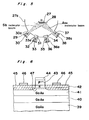
- a substrate holder 27 is situated at the center of a cylindrical vacuum device 27a. Placed on the front surface of the substrate holder 27 is an InP substrate.
- Four cylindrical cells 30, 33, 36 and 38 are disposed so as to radially project from the sylindrical wall of the vacuum device 27a and they are enclosed arm pipes 30a, 33a, 36a and 38a.
- Sb material 29, In material 32 of III group material, Ga material 35 and As material 37 are respectively put in the cells 30, 33, 36 and 38 which are directed toward the substrate holder 27 to radiate respective atomic beams from the materials toward the InP substrate.
- In 0.53 Ga 0.47 As thin Layer of not more than 0.2 p m thick was made using the method of the example 2 in which In molecular beam was used in place of using Ga molecular beam.
- the electron mobility under the room temperature was 10500cm 2 /V.sec., and the carrier density was .1.5 x 10 13 cm 3 . In this case, it was possible to improve the electron characteristics in the thin film layer.
- the same effect could be recognized under the substrate temperature of 300 to 500 °C and it was possible to improve the electron characteristics of In 0.53 Ga 0.47 As thin film layer.
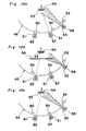
- Ga cell shutter 50 was opened so that Ga material 51 radiated Ga molecular beam and As cell shutter 52 was opened so that As material 53 radiated As molecular beam.
- GaAs layer was grown on the InP substrate laid on the substrate holder 54 for 20 seconds.
- the temperature of the substrate 53 was set at 400 °C to 500 °C.
- a main shutter 56 of a flat plate disposed in from of the substrate 53 was closed to cut off the molecular beams radiated from the cells 51 and 53.
- In cell shutter 60 was opened with the Ga cell shutter 50 closed as shown in Fig. 10 b. This condition was kept for more than about 1 minute. The process mentioned above caused the excessive Ga atoms situated on the most surface of the GaAs thin layer formed on the InP substrate to be released so that a complete planar grown atomic plane could be formed. During this process, Ga cell shutter 50 was closed and In cell shutter 60 was opened, whereby radiation of the impurity gas from Ga cell shutter 50 during reheating thereof could be prevented and fluctuation of the intensity of In molecular beam at the time immediately after the opening of the cell shutter 60 could be suppressed. 61 denotes a Ga material and 62 denotes a Ga cell.
- the main shutter 56 was opened so as to repeat the growth of InAs layer on the thin GaAs layer.
- the same process as mentioned above was repeated for InAs layer and GaAs layer so that alternative InAs layers and GaAs layers each having mono atomic layer super lattice (MSL) were cyclicly formed.
- MSL mono atomic layer super lattice
- a hetero structure as shown in Fig. 12 was prepared wherein each of the interfaces is formed according to the method mentioned above.
- a buffer layer 71 made of Al 0.48 In 0.52 As layer 71, on which a working layer of In 0.53 Ga o.47 As layer , a spacer layer 73 of Al 0.48 In 0.52 As layer and a doping layer 74 of Al 0.48 In 0.52 As layer are respectively formed in turn.
- the condition shown in Fig. 10 b was kept for more than 1 minutes every time the respective interfaces were formed.
- the temperature of the substrate 70 was kept between 400°C and 500°C.
- Fig. 13 the curve X shows the characteristic of the hetero structure according to the present invention and the curve Y shows the characteristic of the hetero structure according to the conventional method. It is understood that the electron mobility of the hetero structure formed by the method according to the present invention is higher than that of the hetero structure made by the conventional method.
- Field effect transistors using MSL consisting of InAs and GaAs made by the present invention and the hetero structure of In 0.53 Ga 0.47 As and Al 0.48 In 0.52 As were also made. They could work with a high speed.
- An advantage of the present invention is to make the time of flattening the surface of the growth layer short by increasing the temperature of the InP substrate in place of keeping the temperature of the substrate constant as mentioned above.
Landscapes
- Chemical & Material Sciences (AREA)
- Engineering & Computer Science (AREA)
- Crystallography & Structural Chemistry (AREA)
- Materials Engineering (AREA)
- Metallurgy (AREA)
- Organic Chemistry (AREA)
- Inorganic Chemistry (AREA)
- Physical Deposition Of Substances That Are Components Of Semiconductor Devices (AREA)
Applications Claiming Priority (6)
| Application Number | Priority Date | Filing Date | Title |
|---|---|---|---|
| JP198878/85 | 1985-09-09 | ||
| JP60198878A JPS6258613A (ja) | 1985-09-09 | 1985-09-09 | 薄膜成長方法 |
| JP200872/85 | 1985-09-10 | ||
| JP60200872A JPS6260218A (ja) | 1985-09-10 | 1985-09-10 | 薄膜成長方法 |
| JP209753/85 | 1985-09-20 | ||
| JP60209753A JPS6269508A (ja) | 1985-09-20 | 1985-09-20 | 化合物半導体装置製造方法 |
Related Child Applications (1)
| Application Number | Title | Priority Date | Filing Date |
|---|---|---|---|
| EP92107691.5 Division-Into | 1986-09-09 |
Publications (3)
| Publication Number | Publication Date |
|---|---|
| EP0215436A2 true EP0215436A2 (fr) | 1987-03-25 |
| EP0215436A3 EP0215436A3 (en) | 1989-02-08 |
| EP0215436B1 EP0215436B1 (fr) | 1993-03-17 |
Family
ID=27327562
Family Applications (2)
| Application Number | Title | Priority Date | Filing Date |
|---|---|---|---|
| EP92107691A Withdrawn EP0499294A1 (fr) | 1985-09-09 | 1986-09-09 | Procédé de croissance moléculaire épitaxiale des couches monocristallines en semi-conducteurs composés |
| EP86112487A Expired - Lifetime EP0215436B1 (fr) | 1985-09-09 | 1986-09-09 | Méthode de croissance d'une couche mince pour semi-conducteur composite |
Family Applications Before (1)
| Application Number | Title | Priority Date | Filing Date |
|---|---|---|---|
| EP92107691A Withdrawn EP0499294A1 (fr) | 1985-09-09 | 1986-09-09 | Procédé de croissance moléculaire épitaxiale des couches monocristallines en semi-conducteurs composés |
Country Status (5)
| Country | Link |
|---|---|
| EP (2) | EP0499294A1 (fr) |
| KR (1) | KR870003552A (fr) |
| CN (2) | CN1004455B (fr) |
| AU (1) | AU590327B2 (fr) |
| DE (1) | DE3688028T2 (fr) |
Cited By (2)
| Publication number | Priority date | Publication date | Assignee | Title |
|---|---|---|---|---|
| EP0250603A4 (fr) * | 1985-12-09 | 1988-11-28 | Nippon Telegraph & Telephone | Procede de formation d'une fine pellicule de semiconducteur compose. |
| KR101282540B1 (ko) * | 2010-11-30 | 2013-07-04 | 미츠비시 쥬고교 가부시키가이샤 | 풍력 발전기 |
Families Citing this family (6)
| Publication number | Priority date | Publication date | Assignee | Title |
|---|---|---|---|---|
| JP3378594B2 (ja) * | 1992-09-25 | 2003-02-17 | 富士通株式会社 | データベース再配置を行う処理装置 |
| US6039809A (en) * | 1998-01-27 | 2000-03-21 | Mitsubishi Materials Silicon Corporation | Method and apparatus for feeding a gas for epitaxial growth |
| US6811814B2 (en) | 2001-01-16 | 2004-11-02 | Applied Materials, Inc. | Method for growing thin films by catalytic enhancement |
| US6838125B2 (en) | 2002-07-10 | 2005-01-04 | Applied Materials, Inc. | Method of film deposition using activated precursor gases |
| CN105986321B (zh) * | 2015-02-16 | 2018-08-28 | 中国科学院苏州纳米技术与纳米仿生研究所 | 在Ge衬底上生长GaAs外延薄膜的方法 |
| CN116145245A (zh) * | 2021-11-21 | 2023-05-23 | 广东众元半导体科技有限公司 | 一种多源在线切换的分子束外延腔体及方法 |
Family Cites Families (7)
| Publication number | Priority date | Publication date | Assignee | Title |
|---|---|---|---|---|
| US3915765A (en) * | 1973-06-25 | 1975-10-28 | Bell Telephone Labor Inc | MBE technique for fabricating semiconductor devices having low series resistance |
| SE393967B (sv) * | 1974-11-29 | 1977-05-31 | Sateko Oy | Forfarande och for utforande av stroleggning mellan lagren i ett virkespaket |
| GB1528192A (en) | 1975-03-10 | 1978-10-11 | Secr Defence | Surface treatment of iii-v compound crystals |
| US4163237A (en) * | 1978-04-24 | 1979-07-31 | Bell Telephone Laboratories, Incorporated | High mobility multilayered heterojunction devices employing modulated doping |
| US4538165A (en) * | 1982-03-08 | 1985-08-27 | International Business Machines Corporation | FET With heterojunction induced channel |
| JPH07120790B2 (ja) * | 1984-06-18 | 1995-12-20 | 株式会社日立製作所 | 半導体装置 |
| US4882609A (en) * | 1984-11-19 | 1989-11-21 | Max-Planck Gesellschaft Zur Forderung Der Wissenschafter E.V. | Semiconductor devices with at least one monoatomic layer of doping atoms |
-
1986
- 1986-09-08 AU AU62456/86A patent/AU590327B2/en not_active Ceased
- 1986-09-09 KR KR1019860007530A patent/KR870003552A/ko not_active Ceased
- 1986-09-09 CN CN86106177.2A patent/CN1004455B/zh not_active Expired
- 1986-09-09 EP EP92107691A patent/EP0499294A1/fr not_active Withdrawn
- 1986-09-09 EP EP86112487A patent/EP0215436B1/fr not_active Expired - Lifetime
- 1986-09-09 DE DE8686112487T patent/DE3688028T2/de not_active Expired - Fee Related
-
1988
- 1988-11-23 CN CN88108172A patent/CN1009885B/zh not_active Expired
Cited By (3)
| Publication number | Priority date | Publication date | Assignee | Title |
|---|---|---|---|---|
| EP0250603A4 (fr) * | 1985-12-09 | 1988-11-28 | Nippon Telegraph & Telephone | Procede de formation d'une fine pellicule de semiconducteur compose. |
| US4829022A (en) * | 1985-12-09 | 1989-05-09 | Nippon Telegraph And Telephone Corporation | Method for forming thin films of compound semiconductors by flow rate modulation epitaxy |
| KR101282540B1 (ko) * | 2010-11-30 | 2013-07-04 | 미츠비시 쥬고교 가부시키가이샤 | 풍력 발전기 |
Also Published As
| Publication number | Publication date |
|---|---|
| AU6245686A (en) | 1987-03-12 |
| DE3688028D1 (de) | 1993-04-22 |
| KR870003552A (ko) | 1987-04-18 |
| EP0215436B1 (fr) | 1993-03-17 |
| AU590327B2 (en) | 1989-11-02 |
| CN1009885B (zh) | 1990-10-03 |
| CN1004455B (zh) | 1989-06-07 |
| EP0215436A3 (en) | 1989-02-08 |
| EP0499294A1 (fr) | 1992-08-19 |
| CN86106177A (zh) | 1987-06-03 |
| CN1032884A (zh) | 1989-05-10 |
| DE3688028T2 (de) | 1993-09-09 |
Similar Documents
| Publication | Publication Date | Title |
|---|---|---|
| US5602418A (en) | Nitride based semiconductor device and manufacture thereof | |
| JP3817206B2 (ja) | 高絶縁性単結晶窒化ガリウム薄膜を有する半導体デバイス | |
| US3751310A (en) | Germanium doped epitaxial films by the molecular beam method | |
| US4960728A (en) | Homogenization anneal of II-VI compounds | |
| EP0127200B1 (fr) | Procédé pour la fabrication d'un dispositif semi-conducteur utilisant la technique des faisceaux moléculaires | |
| EP0875078B1 (fr) | Procede de fabrication d'interface de semiconducteur iii-v/ii-vi | |
| EP0499294A1 (fr) | Procédé de croissance moléculaire épitaxiale des couches monocristallines en semi-conducteurs composés | |
| US4948751A (en) | Moelcular beam epitaxy for selective epitaxial growth of III - V compound semiconductor | |
| US5039626A (en) | Method for heteroepitaxial growth of a two-dimensional material on a three-dimensional material | |
| US4453172A (en) | Field effect transistor with gate insulation of cubic fluoride material | |
| US4831628A (en) | Denices fabricated using method of selective area epitaxial growth using ion beams | |
| US4622093A (en) | Method of selective area epitaxial growth using ion beams | |
| Bosch et al. | Molecular beam epitaxy of InSb (110) | |
| US4233613A (en) | Compound semiconductor wafer | |
| JPS6269508A (ja) | 化合物半導体装置製造方法 | |
| Kuech et al. | Low temperature CVD growth of epitaxial HgTe on CdTe | |
| US5432124A (en) | Method of manufacturing compound semiconductor | |
| Egami et al. | Low‐temperature grain growth of initially< 100> textured polycrystalline silicon films amorphized by silicon ion implantation with normal incident angle | |
| De Jong et al. | Modulation doping structures in silicon by molecular beam epitaxy and off-line ion implantation | |
| JPH0831410B2 (ja) | 半導体装置の製造方法 | |
| JPH0787179B2 (ja) | 超格子半導体装置の製造方法 | |
| WO1990003659A1 (fr) | Fabrication de nanostructures semi-conductrices | |
| JPH05182910A (ja) | 分子線エピタキシャル成長方法 | |
| Aleksandrov et al. | Nucleation of epitaxial films with gas‐transport technique | |
| CN118888635A (zh) | 一种界面电场可调的阻挡杂质带甚长波红外探测器外延方法 |
Legal Events
| Date | Code | Title | Description |
|---|---|---|---|
| PUAI | Public reference made under article 153(3) epc to a published international application that has entered the european phase |
Free format text: ORIGINAL CODE: 0009012 |
|
| AK | Designated contracting states |
Kind code of ref document: A2 Designated state(s): DE FR GB NL |
|
| PUAL | Search report despatched |
Free format text: ORIGINAL CODE: 0009013 |
|
| AK | Designated contracting states |
Kind code of ref document: A3 Designated state(s): DE FR GB NL |
|
| 17P | Request for examination filed |
Effective date: 19890505 |
|
| 17Q | First examination report despatched |
Effective date: 19910502 |
|
| GRAA | (expected) grant |
Free format text: ORIGINAL CODE: 0009210 |
|
| AK | Designated contracting states |
Kind code of ref document: B1 Designated state(s): DE FR GB NL |
|
| XX | Miscellaneous (additional remarks) |
Free format text: TEILANMELDUNG 92107691.5 EINGEREICHT AM 09/09/86. |
|
| REF | Corresponds to: |
Ref document number: 3688028 Country of ref document: DE Date of ref document: 19930422 |
|
| ET | Fr: translation filed | ||
| REG | Reference to a national code |
Ref country code: GB Ref legal event code: 746 Effective date: 19930715 |
|
| REG | Reference to a national code |
Ref country code: FR Ref legal event code: DL |
|
| PLBE | No opposition filed within time limit |
Free format text: ORIGINAL CODE: 0009261 |
|
| STAA | Information on the status of an ep patent application or granted ep patent |
Free format text: STATUS: NO OPPOSITION FILED WITHIN TIME LIMIT |
|
| 26N | No opposition filed | ||
| PGFP | Annual fee paid to national office [announced via postgrant information from national office to epo] |
Ref country code: GB Payment date: 19960902 Year of fee payment: 11 |
|
| PGFP | Annual fee paid to national office [announced via postgrant information from national office to epo] |
Ref country code: FR Payment date: 19960910 Year of fee payment: 11 |
|
| PGFP | Annual fee paid to national office [announced via postgrant information from national office to epo] |
Ref country code: DE Payment date: 19960913 Year of fee payment: 11 |
|
| PGFP | Annual fee paid to national office [announced via postgrant information from national office to epo] |
Ref country code: NL Payment date: 19960930 Year of fee payment: 11 |
|
| PG25 | Lapsed in a contracting state [announced via postgrant information from national office to epo] |
Ref country code: GB Free format text: LAPSE BECAUSE OF NON-PAYMENT OF DUE FEES Effective date: 19970909 |
|
| PG25 | Lapsed in a contracting state [announced via postgrant information from national office to epo] |
Ref country code: FR Free format text: THE PATENT HAS BEEN ANNULLED BY A DECISION OF A NATIONAL AUTHORITY Effective date: 19970930 |
|
| PG25 | Lapsed in a contracting state [announced via postgrant information from national office to epo] |
Ref country code: NL Free format text: LAPSE BECAUSE OF NON-PAYMENT OF DUE FEES Effective date: 19980401 |
|
| GBPC | Gb: european patent ceased through non-payment of renewal fee |
Effective date: 19970909 |
|
| NLV4 | Nl: lapsed or anulled due to non-payment of the annual fee |
Effective date: 19980401 |
|
| PG25 | Lapsed in a contracting state [announced via postgrant information from national office to epo] |
Ref country code: DE Free format text: LAPSE BECAUSE OF NON-PAYMENT OF DUE FEES Effective date: 19980603 |
|
| REG | Reference to a national code |
Ref country code: FR Ref legal event code: ST |