EP0215510A1 - Verarbeitungsgerät zur Beseitigung von verborgenen Seiten für dreidimensionale Bilderzeugung - Google Patents
Verarbeitungsgerät zur Beseitigung von verborgenen Seiten für dreidimensionale Bilderzeugung Download PDFInfo
- Publication number
- EP0215510A1 EP0215510A1 EP86201451A EP86201451A EP0215510A1 EP 0215510 A1 EP0215510 A1 EP 0215510A1 EP 86201451 A EP86201451 A EP 86201451A EP 86201451 A EP86201451 A EP 86201451A EP 0215510 A1 EP0215510 A1 EP 0215510A1
- Authority
- EP
- European Patent Office
- Prior art keywords
- parameters
- polygons
- image
- segments
- coordinates
- Prior art date
- Legal status (The legal status is an assumption and is not a legal conclusion. Google has not performed a legal analysis and makes no representation as to the accuracy of the status listed.)
- Granted
Links
Images




Classifications
-
- G—PHYSICS
- G06—COMPUTING OR CALCULATING; COUNTING
- G06T—IMAGE DATA PROCESSING OR GENERATION, IN GENERAL
- G06T15/00—Three-dimensional [3D] image rendering
- G06T15/10—Geometric effects
- G06T15/40—Hidden part removal
- G06T15/405—Hidden part removal using Z-buffer
Definitions
- the invention relates to a processor of images of objects described in three dimensions, which has means for entering parameters of convex polygons descriptive of these objects in a visualization frame, means for determining, from the parameters of the polygons. , the parameters of the image elements of a two-dimensional transformed image of this object, represented in the display plane of a display device, means for selecting and storing the parameters of all the elements of the most transformed image brought closer to the viewing plane, in order to eliminate the hidden faces of the objects, these being represented from an observation angle chosen from a set of angles.
- It also relates to any system for representing images of objects in three dimensions, using such an image processor.
- Three-dimensional (3D) graphics involves defining the geometry of the object in three dimensions, then moving the object in a coordinate system, finally drawing the object in the plane of a display screen.
- the basic operations of this movement are rotation, translation, scaling, perspective.
- the perspective effect makes it possible to restore the shape of the object in its depth, and this is simulated in a manner analogous to what the human eye perceives.
- the object is first described in a coordinate system, in the form of spatial coordinates, then after the previous displacement operations, this coordinate system is transformed according to the coordinate system of the display device.
- attribute parameters such as om brage, color, texture or transparency which ensure a better rendering of the three-dimensional object on a two-dimensional screen.
- the objects are described according to lines, curves or planes which can themselves be translated into algebraic expressions. According to a widely used procedure, the objects are described according to a set of plane surfaces formed by a series of convex polygons. These must be small enough to represent the curved surfaces adequately.
- the basic method for representing a polygon is to draw up a list of vertex coordinates, the space delimited by the polygons having to be closed. These polygons can then be described for example by plane equations in order to allow the movement of objects in the coordinate system.
- a viewing angle is chosen from which an observer can only observe a certain number of faces of the object, the others being necessarily hidden from him.
- the techniques of representation of three-dimensional images use, to eliminate the hidden faces, the method called "algorithm of depth memory "(Z-buffer in English).
- the principle consists in imagining the display screen in the form of a box of almost infinite depth. The surface of the display screen is broken down into a certain number of image elements regularly distributed in X and in Y. Under the chosen viewing angle, all the polygons are successively analyzed according to this two-dimensional configuration of the elements of picture.
- the stored ZM depth coordinates are initialized with the most distant coordinate admissible by the system. Then the processing of each polygon will be done so that each coordinate Z, associated with each image element contained in a polygon, is compared with the depth coordinate ZM stored in the depth memory. When Z is less than ZM, this ZM coordinate is replaced by the Z coordinate which thus becomes the new ZM coordinate associated with the image element. All the polygons constituting the description of the object are analyzed successively, and are therefore retained for each image element only the ZM data and the attribute parameters C relating only to the points closest to the chosen observation point. . So hidden surfaces are not visible on the screen.
- the attribute parameters associated with each face of the object corresponding to each represented polygon are displayed. These attribute parameters are also stored in an attribute memory. To prevent sudden variations in color or shading from appearing on edges or vertices, you can perform an attribute tween in one or more directions. Thus the attributes are defined for the vertices of each polygon, then the attributes of the intermediate image elements are interpolated to fill the polygon. This makes it possible to give a realistic appearance to the restored image.
- This processing uses the equations of the plane of the polygon, makes the architecture two-dimensional, the coefficients A, B, C, being introduced using a tree structure.
- Such a processor has drawbacks. Firstly, to treat the equation of the plan globally, it is necessary to have a two-dimensional network of basic processing cells. The surface of the integrated circuit is in this case very large. Secondly a consequence of the above is that the operating speed is relatively limited.
- the object of the invention is to eliminate these drawbacks and to define a processor whose operating organization allows very rapid processing of information, with a very small surface occupied on the semiconductor which composes the integrated circuit.
- the invention therefore gives the processor a block structure operating in serial mode, with a pipeline-type processing distributed between the parameters relating to the picture elements: (X, Y), Z, attributes.
- the invention operates an analysis of the line of line display plane.
- another object of the invention is to allow the renewable cyclic introduction of the coordinates and the increments given to the parameters characterizing the polygons.
- the invention as defined in the preamble is remarkable in that it comprises serial processing means, of the pipeline type, of parameters of a set of ble of segments which constitute the intersections of the set of polygons with each display line of the display device, several segments being processed simultaneously, said parameters of the segments being obtained by prior conversion of the parameters of the polygons.
- the parameters of the segments can be introduced bit by bit in the serial processing means of the pipeline type. They can also be entered in groups of bits.
- the set of segment coordinates concerns i segments with 1 ⁇ i ⁇ m or (XM 0i , XN 0i ). Any data of type A (X, Z, ...) linked to segment i propagates successively in the n blocks indicated by k. In each block this datum A k i undergoes elementary processing before its transmission to block k + 1. To simplify the ratings, the segment index i has been omitted above.
- the initial representation of the polygons by their vertices and their edges is transformed into a representation by segments corresponding to the intersection of each polygon with a scanning plane perpendicular to the viewing plane.
- Each polygon Pm, the intersection of which with the display line is not empty, will cut the scanning plane according to a segment.
- the image processor comprises means of serial processing of the pipeline type of the parameters of the segments, to which are supplied the parameters of m polygons Pm converted into a set of segment coordinates (XM 0 , XN 0 ), as well as parameters and increments of depth Zo and dZ 0 , and parameters and increments of attributes C 0 and dC 0 relating to each segment (MO , No ) .
- a vertex of a polygon goes be identified by the coordinates Xu, Yu, Zu, Cu.
- the following increments are defined: where u characterizes a vertex and u + 1 the adjacent vertex.
- Each segment can then be represented by its extreme parameters (XM O , XN 0 ), (ZM O , ZNn), (CM O , CN O ), the analogous consecutive values of the other segments deducing from each other by an increment IX in the direction X, IZ in the direction Z and IC according to the "direction" C.
- XM O , XN 0 extreme parameters
- ZM O , ZNn the analogous consecutive values of the other segments deducing from each other by an increment IX in the direction X, IZ in the direction Z and IC according to the "direction" C.
- dX 1.
- the increment along Z is equal to which is constant for the whole plane and according to C we have:
- the depth register Mp is looped over itself through a multiplexer which allows either to renew the value in memory, or to keep the value previously stored.
- This attribute register is updated at the same time as the depth memory under the control of the same means.
- the data concerning the coordinates XM k , XN k Z k and the attribute C k are processed by the processor according to a pipeline-type procedure.
- the set of n consecutive basic cells, which process an entire line of the display device, are connected to a data output bus which transmits the attribute information from the image processor to a display device.
- the parameters of the polygons are supplied to the image processor in the form of segments (M 0 , N 0 ) which are determined by software processed by a computer connected to the image processor.
- the polygons are converted into segments XMn, XN O using a circuit for converting polygons into segments.
- the invention relates to a scene image processor described in three dimensions, comprising a circuit for converting polygons into segments and serial processing means, of pipeline type, of the parameters of the segments.
- This circuit reads in an image memory the coordinates and the attributes relating to each polygon such as for example that will be indicated later on TABLE 1.
- the principle of this circuit is to circulate all the variables X, (respectively Z), (respectively C) in a shift register at the end of which is placed a cell adding the outgoing data with the data IX, (respectively IZ), (respectively IC) read in the image memory.
- the length of the shift register is constant and can contain a determined number of descriptive parameters of polygons.
- control of the sequencing of the shift register is carried out using a control circuit which takes into account the end of edge and end of polygon tests, and which also controls the operation of an address sequencer. which controls the readings from the image memory, which makes it possible to renew the polygons loaded in the shift register as the data processing proceeds.
- the left and right vertices are identical, point A in the example. In cases by particular where the first edge encountered is parallel to the plane Q, the left and right vertices are different.
- the presentation of an image on a screen requires the definition of a scan plan of the image to ensure a sequential processing of the operations.
- This scanning plane is identified by the letter Q in the drawing of FIG. 1 in the frame XYZ, where the direction Z indicates the direction perpendicular to the screen, behind it.
- the polygon ABCD intersects the plane Q along the segment MN.
- the successive scanning planes will each time cut the polygon ABCD according to segments MN, M'N ', etc.
- the point N' is distant from the point N such that IYN - YN '
- Each scan plane determines each time a line of visualization on the screen.
- the image processor therefore operates the processing of the coordinates XM, XN, Z, the increments dZ 0 and dC 0 and the attribute C concerning all the segments MONO of all the polygons ABCD describing the object.
- the block diagram of the serial processing means of the image processor is shown in FIG. 2.
- the coordinates XM O , XN O of the segment MONO are introduced with the least significant bit at the head in a decrementer 10 1 which subtracts a binary unit from the data.
- the part of the circuit consisting of the decrementer 10 1 , the validation member 11 1 and the base cell 12 1 is repeated n times consecutively (n, number of picture elements in a display line).
- the output of the decrementer 10 1 is connected to the input of the decrementer 10 2 which performs the same type of operation but on the coordinates XM 1 , XN 1 . This is repeated until the 10 n decrementer.
- the validation bodies 11 2 ... 11 n are respectively assigned to the decrementers 10 2 ... 10 n and perform the same tests as the validation body 11 1 .
- the validation bodies 11 1 to 11 n thus respectively control the operation of the basic cells 12 1 to 12 n .
- the decrementers in combination with their respective validation unit are used to determine the position of the segment in the line of visualization being processed.
- the basic cell 12 also receives the data dZ 0 and dC 0 which characterize the segment-specific increments, the data Z 0 and C 0 which characterize the coordinate and the color attribute of the origin of the segment and a signal OE 0 end of line exploration for viewing and initialization of the next line.
- This initialization is carried out by forcing the updating of the parameters Z and C by those of the first re-entrant segment which constitutes the background segment.
- the data XM 0 , XN O , Z 0 , dZ 0 , C 0 , dC 0 are supplied to the serial processing means, of the pipeline type, of the image processor, by means 40 for converting parameters of polygons into parameters of segments.
- the attribute results determined by each basic cell 12 1 ... 12 k ... 12 n are read using an output bus 13.
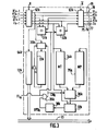
- FIG. 3 represents the block diagram of a basic cell of FIG. 2 constituting the means for processing the depth coordinates and attributes of the image processor.
- the kth base cell 12 k receives, from the base cell which precedes it, the signals Z k - 1 , dZ k - 1 , C k - 1 , dC k-1 , and transmits to the base cell which follows it the signals Z k , dZ k , C k , dC k .
- the kth basic cell 12 k also receives the signal FLk .
- the signals Ck-1 , dCk-1 , Zk-1 , dZk-1 and OE k - 1 enter on a flip-flop with five inputs 62k, controlled by a clock H, respectively on the connections 77, 78, 75, 76, 79 Likewise, the signals C k , dC k , Z k , dZ k and OE k leave a flip-flop with five inputs 63k controlled by the clock H.
- the signal OE k is triggered on the last segment of the line of viewing during processing. For reasons of simplification of writing, the same designation is kept in each case for these different signals on either side of each of the flip-flops.
- the signals Z k-1 and dZ k-1 enter an adder 32 k which performs the operation under the control of the signal FL k from the validation device.
- the value Z k - 1 enters a temporary register MT 34 k .
- the result of the addition Z k Z k - l + FL k .dZ k-1 leaves the basic cell 12 k via connection 75 to be introduced into the following basic cell 12 k + 1 .
- the output of the temporary register MT 34 k enters a 36 k multiplexer whose output enters a depth register MP 35 k .
- the output of the multiplexer 36 k also enters a comparator 37 k which also receives Z k-1 and delivers a comparison signal UPD k which is stored in the flip-flop 38 k .
- the 34k and 35k registers are shift registers.
- the 36 k multiplexer is shown in the Figure 4. It consists of an AND gate 74 k which performs the logical AND operation between the test signal CN k from the gate 39 k and the output of the register 34 k .
- the test signal CN k is inverted by the inverter 73 k , the output of which enters an AND gate 71 k with the output of the register 35 k .
- the outputs of AND gates 71 k and 74 k enter an OR gate 72 k , the output of which enters the register 35 k .
- the AND gate 39 k receives the signal FL k and the output of the flip-flop 38 k .
- the output of the AND gate 39 k controls the operation of a 30 k selector which receives the attribute C k _ 1 ⁇
- the data contained in the attribute register 33 k are placed on a parallel bus 13 common to all the cells via a three-state output circuit 64 k controlled by the signal OE k - 1 . It is also possible to output the color in sequenced serial mode.
- the 34 k and 35 k shift registers synchronize the data stored there.
- the depth register 35 k being looped back on itself via the multiplexer 36 k already indicated, the information that it contains will therefore either be able to reappear regularly on its output, or be replaced by that coming from the register 34k.
- the depth register MP 35 k stores all the information Zc k selected by the multiplexer 36k, after the refresh operation has been carried out and reinserts them cyclically in the comparison procedure until the set of segments for l all the points on the screen have been tested.
- the attribute register 33 k is not subject to any comparison procedure, and stores the attributes C k-1 , for the entire line, under the control of the decision taken for the depth value Z k-1 .
- the mode of operation of the processor-type serial processing means of the processor is as follows.
- the index of the element d image E r and that of the cycle T r are arbitrarily chosen to be identical.
- T r + 1 the operations on the data XM r + 1 and XN r + 1 are carried out simultaneously with the operations on the depth dimension Z r .
- T r + 2 the operations on the data XM r + 2 and XN r + 2 are carried out simultaneously with the operations on the depth dimension Z r + 1 and on the attribute C r .
- This triple pipeline mode allows operations to be carried out in a short time.
- the signal OE k forces the output UPD k of the comparator 38 k to 1, which causes the loading of the parameters Z and C of the background segment.
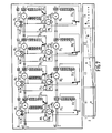
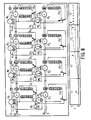
- FIGS. 6, 7 and 8 show the state of these means at the end of three successive steps.
- XM o and XN o are coded on 3 bits and Z o , dZ o , C o and dC o are coded on 6 bits.
- a basic cycle T corresponding to the processing time of a segment, therefore includes 6 elementary clock periods.
- Each elementary cell is assigned to an image point.
- the elementary cell of index 2 is assigned to the image point E2.
- the corresponding references used in the previous electrical diagrams are shown in these illustrations.
- Segment V is treated first.
- the decrementers 10 1 , 10 2 , 10 3 , 10 4 operate on XM o and XN o , and the flags FL 1 , FL 2 , FL 3 , FL 4 are positioned successively at 1 since 4 image points are concerned, and validate segment V in cells E1, E2, E3, E4 at the end of the first cycle time T1.
- FIG. 6 represents the state at the end of the following cycle T2 relative to the cell E1.
- the positions of the flags FL 1 , FL 2 , FL 3 , FL 4 for the segment V are gradually transferred to the flags FL 1 M, FL 2 M, FL 3 M, FL 4 M which keep the positions which will be used with a shift cycle.
- the segment V having previously been validated, the operation Z V + dZ V is carried out, and the result stored in the memories 34 1 , 34 2 , 34 3 , 34 4 .
- the signals UPD k are then presented to the AND gates 39 k to form, with the flags FL k , the signals CN k which will then determine the position of the multiplexers at the output of the registers 34 k and 35 k .
- the decrementers operate on segment B.
- the cells E1, E2, E3 are not concerned.
- the E4 cell is concerned.
- the flags FL 1 , FL 2 and FL 3 are positioned gradually born at 0 in cells E1, E2 and E3, then the flag FL 4 at 1 in cell E4.
- the calculation Z A + dZ A is performed for the seg ment A and compared with the values Z V stored in registers 35 2 and 35 3 of cells E2 and E3, since for segment A only the calculation in cells E2 and E3 is validated.
- Cy + dCy is calculated for segment V in cells E1, E2, E3, E4. Since for the segment V the different flags FL k had the value 1 and since the different signals CN k were also 1, the values Cy + dCy will be stored in the memories 3 3 k.
- FIG. 7 represents the state at the end of the following T4 cycle relative to the cell E1.
- cells E2 and E3 the flags FL 2 M and FL 3 M and the flags UPD2 and UPD3 being positioned at 1, CN 2 and CN 3 are also positioned at 1 and they control the multiplexers in order to substitute in cells E 2 and E 3 Zy of segment V by Z A of segment A because Z A is less than Zy.
- the calculation C A + dC A is carried out in cells E2 and E3 because FL 2 M and FL 3 M are positioned at 1 (cells concerned by this segment). FL 1 M and FL 4 M are positioned at 0. The addition is therefore not made, but the updating is carried out in cells E2 and E3 because CN 2 and CN 3 are positioned at 1.
- FIG. 8 represents the state at the end of the following T5 cycle relative to the cell E1.
- serial processing means of pipeline type, to which are supplied parameters of polygons previously converted according to parameters of a set of segments (M O , N 0 ).
- the conversion means then consist of software operating on a computer, a microcomputer or a microprocessor which also operates the storage of basic data.
- the serial processing means of the pipeline type are then combined, for example in the form of an integrated circuit, and then constitute the image processor according to the invention. It is then connected to a display processor which supplies the restored image.
- the conversion means consist of a circuit for converting parameters of polygons into parameters of segments.
- This can constitute an independent circuit in the form for example of an integrated circuit.
- the image processor then comprises serial processing means, of the pipeline type, and said conversion circuit which receives its basic data from an image memory which stores the parameters of the polygons.
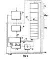
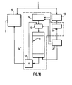
- FIG. 9 represents the block diagram of the conversion means constituted by a conversion circuit 40. They comprise an adder 27 which receives on one input the output of an input register 43 and on the other input the output d a circulating memory 22 which receives on its input the output of the adder 27.
- the circulating memory 22 can consist of a shift register in order to operate in synchronism with the serial processing means of the pipeline type. It stores the DPp information relating to each polygon Pp intercepted by the display line.
- the input register 43 receives the parameters of the polygons from an image memory 25 previously loaded from the outside. The loading of the input register 43 is controlled by a control and test circuit 42 which controls the operation of the conversion circuit as well as the calls to read the image memory through a sequencer 24.
- the parameters of the polygons are stored in the image memory for example with the nature and the ordering of the parameters indicated in table 1 above.
- the commands (RAZO) 47 and (RAZ) 48 the input register 43 and the circulating memory 22 are set to zero in order to initialize the loading of the data.
- the command (LOAD) 45 performs the loading of the input register 43.
- the sequencer 24 receives a command 81 from the test and control circuit 42 which will cause the reading of data in the image memory.
- These data will be transmitted through the input register 43 and the adder 27 to the circulating memory 22 which will thus be loaded with dZ, CM O , XM O , LYd, ZN O , CN O , XN O , LYg of the polygon.
- this memory 22 Since this memory 22 operates in a loop, it is necessary to give it a sufficient size but not excessive so as not to lengthen the duration of the treatment. With the number of parameters selected for each polygon such as those indicated in Table 1, the possibility of storing 32 polygons is an acceptable dimension. It allows processing in real time.
- the dZ parameter of a polygon is a constant for each polygon and must not be modified. However, for reasons of simplification of processing, it is introduced into the parameters of the polygons, but its passage through the adder 27 does not alter it by positioning the output of the input register 43 at zero using the command. RESET 47.
- the control and test circuit 42 performs the test of the length of the right and left edges of the polygons. When after processing the circulating length LY reaches the value zero, the edge concerned has finished being used and must be replaced by the next edge if the polygon has not finished being processed, or by a new polygon otherwise.
- a multiplexer 53 selects the output of an input battery 54 or that of an adder 52 under the control of the control and test circuit 42. The operations are sequenced as follows.
- a line counter 56 is incremented on each line.
- the addresses of the polygons starting at this line are loaded into the input stack 54. These addresses are generated externally in the generator 55 which receives instructions from a central unit.
- An offset is made to the address register 51 every 8 elementary clock periods, which corresponds to the following 8 operations for processing the polygon: So every 8 elementary clock periods u, which corresponds to the determination of the parameters of the segment determined by the intersection of the polygon with the display line, a new polygon address is presented at the output of the register 51 to process the polygon following.
- the address sequencer 24 then generates the addresses of the various data sought in the image memory. This sequence of addresses is linked to the values of the flags PA, DP, Dg, Dd. These read data are then sent to the input register 43.
- the address word stored in the register 51 for each polygon first presents a first field constituted killed by APp, Narg, Ng, Nard, Nd, (APp polygon index) which generates the addresses of the data and a second field consisting of PA, DP, Dd, Dg which indicate the state of the polygon.
- This register 51 stores one address word per polygon having the composition:
- each processor delivers not only the parameters C, but also the parameters Z, by simultaneously and separately processing two sets of segments relating to the same display line.
- a comparison of the Z parameters makes it possible to make a selection of the color to be displayed.
- a transparency flag can be assigned to a segment which intervenes on the signals CN k to inhibit, for example one clock out of two, the updating of the parameters Z k and C k of the transparent segment.
Landscapes
- Physics & Mathematics (AREA)
- Engineering & Computer Science (AREA)
- Geometry (AREA)
- Computer Graphics (AREA)
- General Physics & Mathematics (AREA)
- Theoretical Computer Science (AREA)
- Image Generation (AREA)
- Processing Or Creating Images (AREA)
Applications Claiming Priority (2)
| Application Number | Priority Date | Filing Date | Title |
|---|---|---|---|
| FR8512925A FR2586838B1 (fr) | 1985-08-30 | 1985-08-30 | Processeur d'elimination de faces cachees pour la synthese d'images a trois dimensions |
| FR8512925 | 1985-08-30 |
Publications (2)
| Publication Number | Publication Date |
|---|---|
| EP0215510A1 true EP0215510A1 (de) | 1987-03-25 |
| EP0215510B1 EP0215510B1 (de) | 1993-07-07 |
Family
ID=9322498
Family Applications (1)
| Application Number | Title | Priority Date | Filing Date |
|---|---|---|---|
| EP86201451A Expired - Lifetime EP0215510B1 (de) | 1985-08-30 | 1986-08-22 | Verarbeitungsgerät zur Beseitigung von verborgenen Seiten für dreidimensionale Bilderzeugung |
Country Status (5)
| Country | Link |
|---|---|
| US (1) | US4812988A (de) |
| EP (1) | EP0215510B1 (de) |
| JP (1) | JPH0727580B2 (de) |
| DE (1) | DE3688665T2 (de) |
| FR (1) | FR2586838B1 (de) |
Cited By (3)
| Publication number | Priority date | Publication date | Assignee | Title |
|---|---|---|---|---|
| EP0360903A1 (de) * | 1988-09-29 | 1990-04-04 | Kabushiki Kaisha Toshiba | Steuergerät des die Tiefeninformation enthaltenden Buffers |
| EP0314368A3 (de) * | 1987-10-26 | 1991-02-06 | Tektronix, Inc. | Verfahren und Gerät zur Wegnahme von verborgenen Flächen |
| EP0425186A3 (en) * | 1989-10-23 | 1993-02-03 | International Business Machines Corporation | Z-buffer control |
Families Citing this family (47)
| Publication number | Priority date | Publication date | Assignee | Title |
|---|---|---|---|---|
| IL84936A (en) * | 1987-12-23 | 1997-02-18 | Cubital Ltd | Three-dimensional modelling apparatus |
| JPS63271673A (ja) * | 1987-04-30 | 1988-11-09 | Toshiba Corp | 三次元表示装置 |
| JP2653078B2 (ja) * | 1987-05-25 | 1997-09-10 | セイコーエプソン株式会社 | 画像表示制御装置及びこれを具備する電子機器 |
| JPH0634209B2 (ja) * | 1987-07-23 | 1994-05-02 | 株式会社日立製作所 | 表示図形検知方式 |
| US5265214A (en) * | 1987-08-28 | 1993-11-23 | Daikin Industries, Ltd. | Filling processing apparatus and method |
| US4918626A (en) * | 1987-12-09 | 1990-04-17 | Evans & Sutherland Computer Corp. | Computer graphics priority system with antialiasing |
| US5276783A (en) * | 1989-11-21 | 1994-01-04 | International Business Machines Corporation | Tessellating complex polygons in modeling coordinates |
| US5245700A (en) * | 1989-11-21 | 1993-09-14 | International Business Machines Corporation | Adjustment of z-buffer values for lines on the surface of a polygon |
| EP0449478A3 (en) * | 1990-03-29 | 1992-11-25 | Microtime Inc. | 3d video special effects system |
| US5220646A (en) * | 1990-04-30 | 1993-06-15 | International Business Machines Corporation | Single pass hidden line removal using z-buffers |
| JPH07120435B2 (ja) * | 1990-12-06 | 1995-12-20 | インターナショナル・ビジネス・マシーンズ・コーポレイション | 高速zバッファの初期化および更新方法ならびにそのシステム |
| CA2060975C (en) * | 1991-02-25 | 1998-11-10 | Gopalan Ramanujam | Scientific visualization system |
| US5821940A (en) * | 1992-08-03 | 1998-10-13 | Ball Corporation | Computer graphics vertex index cache system for polygons |
| US5973700A (en) * | 1992-09-16 | 1999-10-26 | Eastman Kodak Company | Method and apparatus for optimizing the resolution of images which have an apparent depth |
| JP2710202B2 (ja) * | 1993-03-24 | 1998-02-10 | インターナショナル・ビジネス・マシーンズ・コーポレイション | 閉じた輪郭イメージを凸多角形で境界づける方法及びデータ処理装置 |
| GB9316214D0 (en) * | 1993-08-05 | 1993-09-22 | Philips Electronics Uk Ltd | Image processing |
| US5974539A (en) * | 1993-11-30 | 1999-10-26 | Texas Instruments Incorporated | Three input arithmetic logic unit with shifter and mask generator |
| US6116768A (en) * | 1993-11-30 | 2000-09-12 | Texas Instruments Incorporated | Three input arithmetic logic unit with barrel rotator |
| US6098163A (en) * | 1993-11-30 | 2000-08-01 | Texas Instruments Incorporated | Three input arithmetic logic unit with shifter |
| US5590350A (en) * | 1993-11-30 | 1996-12-31 | Texas Instruments Incorporated | Three input arithmetic logic unit with mask generator |
| US5961635A (en) * | 1993-11-30 | 1999-10-05 | Texas Instruments Incorporated | Three input arithmetic logic unit with barrel rotator and mask generator |
| US5560030A (en) * | 1994-03-08 | 1996-09-24 | Texas Instruments Incorporated | Transfer processor with transparency |
| US5651127A (en) * | 1994-03-08 | 1997-07-22 | Texas Instruments Incorporated | Guided transfers with variable stepping |
| US5487146A (en) * | 1994-03-08 | 1996-01-23 | Texas Instruments Incorporated | Plural memory access address generation employing guide table entries forming linked list |
| US5493646A (en) * | 1994-03-08 | 1996-02-20 | Texas Instruments Incorporated | Pixel block transfer with transparency |
| WO1997044776A2 (en) * | 1996-05-17 | 1997-11-27 | Philips Electronics N.V. | Display device |
| US6618048B1 (en) | 1999-10-28 | 2003-09-09 | Nintendo Co., Ltd. | 3D graphics rendering system for performing Z value clamping in near-Z range to maximize scene resolution of visually important Z components |
| US7119813B1 (en) | 2000-06-02 | 2006-10-10 | Nintendo Co., Ltd. | Variable bit field encoding |
| US7538772B1 (en) | 2000-08-23 | 2009-05-26 | Nintendo Co., Ltd. | Graphics processing system with enhanced memory controller |
| US6825851B1 (en) | 2000-08-23 | 2004-11-30 | Nintendo Co., Ltd. | Method and apparatus for environment-mapped bump-mapping in a graphics system |
| US6700586B1 (en) | 2000-08-23 | 2004-03-02 | Nintendo Co., Ltd. | Low cost graphics with stitching processing hardware support for skeletal animation |
| US6707458B1 (en) | 2000-08-23 | 2004-03-16 | Nintendo Co., Ltd. | Method and apparatus for texture tiling in a graphics system |
| US7184059B1 (en) | 2000-08-23 | 2007-02-27 | Nintendo Co., Ltd. | Graphics system with copy out conversions between embedded frame buffer and main memory |
| US7034828B1 (en) | 2000-08-23 | 2006-04-25 | Nintendo Co., Ltd. | Recirculating shade tree blender for a graphics system |
| US7002591B1 (en) | 2000-08-23 | 2006-02-21 | Nintendo Co., Ltd. | Method and apparatus for interleaved processing of direct and indirect texture coordinates in a graphics system |
| US6636214B1 (en) | 2000-08-23 | 2003-10-21 | Nintendo Co., Ltd. | Method and apparatus for dynamically reconfiguring the order of hidden surface processing based on rendering mode |
| US6980218B1 (en) * | 2000-08-23 | 2005-12-27 | Nintendo Co., Ltd. | Method and apparatus for efficient generation of texture coordinate displacements for implementing emboss-style bump mapping in a graphics rendering system |
| US6937245B1 (en) * | 2000-08-23 | 2005-08-30 | Nintendo Co., Ltd. | Graphics system with embedded frame buffer having reconfigurable pixel formats |
| US7061502B1 (en) | 2000-08-23 | 2006-06-13 | Nintendo Co., Ltd. | Method and apparatus for providing logical combination of N alpha operations within a graphics system |
| US6867781B1 (en) | 2000-08-23 | 2005-03-15 | Nintendo Co., Ltd. | Graphics pipeline token synchronization |
| US7576748B2 (en) * | 2000-11-28 | 2009-08-18 | Nintendo Co. Ltd. | Graphics system with embedded frame butter having reconfigurable pixel formats |
| US6811489B1 (en) | 2000-08-23 | 2004-11-02 | Nintendo Co., Ltd. | Controller interface for a graphics system |
| US7891818B2 (en) | 2006-12-12 | 2011-02-22 | Evans & Sutherland Computer Corporation | System and method for aligning RGB light in a single modulator projector |
| US8358317B2 (en) | 2008-05-23 | 2013-01-22 | Evans & Sutherland Computer Corporation | System and method for displaying a planar image on a curved surface |
| US8702248B1 (en) | 2008-06-11 | 2014-04-22 | Evans & Sutherland Computer Corporation | Projection method for reducing interpixel gaps on a viewing surface |
| US8077378B1 (en) | 2008-11-12 | 2011-12-13 | Evans & Sutherland Computer Corporation | Calibration system and method for light modulation device |
| US9641826B1 (en) | 2011-10-06 | 2017-05-02 | Evans & Sutherland Computer Corporation | System and method for displaying distant 3-D stereo on a dome surface |
Citations (1)
| Publication number | Priority date | Publication date | Assignee | Title |
|---|---|---|---|---|
| FR2406927A1 (fr) * | 1977-10-19 | 1979-05-18 | Inst Avtomatiki Elektrometri | Dispositif de production des images en noir et blanc ou en couleur d'objets tridimensionnels sur ecran de television en temps reel |
Family Cites Families (8)
| Publication number | Priority date | Publication date | Assignee | Title |
|---|---|---|---|---|
| US4208719A (en) * | 1978-08-10 | 1980-06-17 | The Singer Company | Edge smoothing for real-time simulation of a polygon face object system as viewed by a moving observer |
| US4529978A (en) * | 1980-10-27 | 1985-07-16 | Digital Equipment Corporation | Method and apparatus for generating graphic and textual images on a raster scan display |
| US4590465A (en) * | 1982-02-18 | 1986-05-20 | Henry Fuchs | Graphics display system using logic-enhanced pixel memory cells |
| US4570233A (en) * | 1982-07-01 | 1986-02-11 | The Singer Company | Modular digital image generator |
| US4667190A (en) * | 1982-07-30 | 1987-05-19 | Honeywell Inc. | Two axis fast access memory |
| GB8411579D0 (en) * | 1984-05-05 | 1984-06-13 | Ibm | Graphic display systems |
| US4758965A (en) * | 1985-10-09 | 1988-07-19 | International Business Machines Corporation | Polygon fill processor |
| IL79822A (en) * | 1985-12-19 | 1990-03-19 | Gen Electric | Method of comprehensive distortion correction for a computer image generation system |
-
1985
- 1985-08-30 FR FR8512925A patent/FR2586838B1/fr not_active Expired
-
1986
- 1986-08-22 DE DE86201451T patent/DE3688665T2/de not_active Expired - Fee Related
- 1986-08-22 EP EP86201451A patent/EP0215510B1/de not_active Expired - Lifetime
- 1986-08-29 JP JP61201913A patent/JPH0727580B2/ja not_active Expired - Lifetime
- 1986-08-29 US US06/902,372 patent/US4812988A/en not_active Expired - Fee Related
Patent Citations (1)
| Publication number | Priority date | Publication date | Assignee | Title |
|---|---|---|---|---|
| FR2406927A1 (fr) * | 1977-10-19 | 1979-05-18 | Inst Avtomatiki Elektrometri | Dispositif de production des images en noir et blanc ou en couleur d'objets tridimensionnels sur ecran de television en temps reel |
Cited By (3)
| Publication number | Priority date | Publication date | Assignee | Title |
|---|---|---|---|---|
| EP0314368A3 (de) * | 1987-10-26 | 1991-02-06 | Tektronix, Inc. | Verfahren und Gerät zur Wegnahme von verborgenen Flächen |
| EP0360903A1 (de) * | 1988-09-29 | 1990-04-04 | Kabushiki Kaisha Toshiba | Steuergerät des die Tiefeninformation enthaltenden Buffers |
| EP0425186A3 (en) * | 1989-10-23 | 1993-02-03 | International Business Machines Corporation | Z-buffer control |
Also Published As
| Publication number | Publication date |
|---|---|
| US4812988A (en) | 1989-03-14 |
| DE3688665D1 (de) | 1993-08-12 |
| DE3688665T2 (de) | 1994-02-03 |
| FR2586838A1 (fr) | 1987-03-06 |
| JPH0727580B2 (ja) | 1995-03-29 |
| JPS6252682A (ja) | 1987-03-07 |
| EP0215510B1 (de) | 1993-07-07 |
| FR2586838B1 (fr) | 1989-07-28 |
Similar Documents
| Publication | Publication Date | Title |
|---|---|---|
| EP0215510B1 (de) | Verarbeitungsgerät zur Beseitigung von verborgenen Seiten für dreidimensionale Bilderzeugung | |
| Georgoulis et al. | Reflectance and natural illumination from single-material specular objects using deep learning | |
| WO2021164759A1 (en) | Three-dimensional facial reconstruction | |
| EP0458692B1 (de) | Verfahren zur Anzeige eines Bildteiles einer physikalischen Struktur | |
| Carr et al. | Fast GPU ray tracing of dynamic meshes using geometry images. | |
| Bar-Joseph et al. | Texture mixing and texture movie synthesis using statistical learning | |
| Yang et al. | The cluster hair model | |
| FR2583541A1 (fr) | Tampon z a haute vitesse munie d'une memoire dynamique a acces aleatoire | |
| EP4064131A1 (de) | Bilddarstellungsverfahren und -vorrichtung | |
| FR2542470A1 (fr) | Systeme de machine a calculer a multiprocesseur pour convertir des elements-objets definis dans une structure de donnees hierarchique en une representation visuelle coloree | |
| EP4095807A1 (de) | Bildsynthese unter benutzung mehrerer modelle maschinellen lernens | |
| Spick et al. | Naive mesh-to-mesh coloured model generation using 3D GANs | |
| Guennebaud et al. | Deferred splatting | |
| WO2005083671A1 (en) | Using polynomial texture maps for micro-scale occlusions | |
| FR2689272A1 (fr) | Dispositif de traitement d'informations d'images tridimensionnelles, avec extraction de lignes remarquables. | |
| JP2006517705A (ja) | コンピュータグラフィックスシステム及びコンピュータグラフィクイメージのレンダリング方法 | |
| US20240161362A1 (en) | Target-augmented material maps | |
| Kang et al. | Efficient randomized hierarchy construction for interactive visualization of large scale point clouds | |
| EP0368718B1 (de) | Verfahren zur Auswahl eines Objektes in einem n-dimensionalen Referenzsystem und Anzeige des ausgewählten Objektes | |
| CN118247412B (zh) | 材质及三维模型重建方法、装置 | |
| KR100693134B1 (ko) | 3차원 이미지 처리 | |
| CN118864676A (zh) | 三维模型生成方法及装置、计算机程序产品和电子设备 | |
| Gerhards et al. | Partitioned shadow volumes | |
| EP4080462A1 (de) | Bilddarstellungsverfahren und -vorrichtung | |
| Willcocks | Sparse volumetric deformation |
Legal Events
| Date | Code | Title | Description |
|---|---|---|---|
| PUAI | Public reference made under article 153(3) epc to a published international application that has entered the european phase |
Free format text: ORIGINAL CODE: 0009012 |
|
| AK | Designated contracting states |
Kind code of ref document: A1 Designated state(s): DE FR GB IT SE |
|
| 17P | Request for examination filed |
Effective date: 19870702 |
|
| 17Q | First examination report despatched |
Effective date: 19881207 |
|
| RAP1 | Party data changed (applicant data changed or rights of an application transferred) |
Owner name: LABORATOIRES D'ELECTRONIQUE PHILIPS Owner name: N.V. PHILIPS' GLOEILAMPENFABRIEKEN |
|
| GRAA | (expected) grant |
Free format text: ORIGINAL CODE: 0009210 |
|
| AK | Designated contracting states |
Kind code of ref document: B1 Designated state(s): DE FR GB IT SE |
|
| PG25 | Lapsed in a contracting state [announced via postgrant information from national office to epo] |
Ref country code: IT Free format text: LAPSE BECAUSE OF FAILURE TO SUBMIT A TRANSLATION OF THE DESCRIPTION OR TO PAY THE FEE WITHIN THE PRE;WARNING: LAPSES OF ITALIAN PATENTS WITH EFFECTIVE DATE BEFORE 2007 MAY HAVE OCCURRED AT ANY TIME BEFORE 2007. THE CORRECT EFFECTIVE DATE MAY BE DIFFERENT FROM THE ONE RECORDED.SCRIBED TIME-LIMIT Effective date: 19930707 Ref country code: SE Effective date: 19930707 |
|
| REF | Corresponds to: |
Ref document number: 3688665 Country of ref document: DE Date of ref document: 19930812 |
|
| GBT | Gb: translation of ep patent filed (gb section 77(6)(a)/1977) |
Effective date: 19931004 |
|
| PLBE | No opposition filed within time limit |
Free format text: ORIGINAL CODE: 0009261 |
|
| STAA | Information on the status of an ep patent application or granted ep patent |
Free format text: STATUS: NO OPPOSITION FILED WITHIN TIME LIMIT |
|
| 26N | No opposition filed | ||
| REG | Reference to a national code |
Ref country code: FR Ref legal event code: CD Ref country code: FR Ref legal event code: CJ |
|
| PGFP | Annual fee paid to national office [announced via postgrant information from national office to epo] |
Ref country code: GB Payment date: 19960731 Year of fee payment: 11 |
|
| PGFP | Annual fee paid to national office [announced via postgrant information from national office to epo] |
Ref country code: FR Payment date: 19960828 Year of fee payment: 11 |
|
| PGFP | Annual fee paid to national office [announced via postgrant information from national office to epo] |
Ref country code: DE Payment date: 19961025 Year of fee payment: 11 |
|
| PG25 | Lapsed in a contracting state [announced via postgrant information from national office to epo] |
Ref country code: GB Free format text: LAPSE BECAUSE OF NON-PAYMENT OF DUE FEES Effective date: 19970822 |
|
| GBPC | Gb: european patent ceased through non-payment of renewal fee |
Effective date: 19970822 |
|
| PG25 | Lapsed in a contracting state [announced via postgrant information from national office to epo] |
Ref country code: FR Free format text: LAPSE BECAUSE OF NON-PAYMENT OF DUE FEES Effective date: 19980430 |
|
| PG25 | Lapsed in a contracting state [announced via postgrant information from national office to epo] |
Ref country code: DE Free format text: LAPSE BECAUSE OF NON-PAYMENT OF DUE FEES Effective date: 19980501 |
|
| REG | Reference to a national code |
Ref country code: FR Ref legal event code: ST |