EP0216066A2 - Synchronisiersystem für digitale Informationsübertragung - Google Patents
Synchronisiersystem für digitale Informationsübertragung Download PDFInfo
- Publication number
- EP0216066A2 EP0216066A2 EP86110157A EP86110157A EP0216066A2 EP 0216066 A2 EP0216066 A2 EP 0216066A2 EP 86110157 A EP86110157 A EP 86110157A EP 86110157 A EP86110157 A EP 86110157A EP 0216066 A2 EP0216066 A2 EP 0216066A2
- Authority
- EP
- European Patent Office
- Prior art keywords
- bits
- bit
- field
- sync
- signal
- Prior art date
- Legal status (The legal status is an assumption and is not a legal conclusion. Google has not performed a legal analysis and makes no representation as to the accuracy of the status listed.)
- Withdrawn
Links
Images



Classifications
-
- H—ELECTRICITY
- H04—ELECTRIC COMMUNICATION TECHNIQUE
- H04L—TRANSMISSION OF DIGITAL INFORMATION, e.g. TELEGRAPHIC COMMUNICATION
- H04L25/00—Baseband systems
- H04L25/38—Synchronous or start-stop systems, e.g. for Baudot code
- H04L25/40—Transmitting circuits; Receiving circuits
- H04L25/49—Transmitting circuits; Receiving circuits using code conversion at the transmitter; using predistortion; using insertion of idle bits for obtaining a desired frequency spectrum; using three or more amplitude levels ; Baseband coding techniques specific to data transmission systems
-
- H—ELECTRICITY
- H04—ELECTRIC COMMUNICATION TECHNIQUE
- H04L—TRANSMISSION OF DIGITAL INFORMATION, e.g. TELEGRAPHIC COMMUNICATION
- H04L7/00—Arrangements for synchronising receiver with transmitter
- H04L7/04—Speed or phase control by synchronisation signals
- H04L7/041—Speed or phase control by synchronisation signals using special codes as synchronising signal
-
- H—ELECTRICITY
- H04—ELECTRIC COMMUNICATION TECHNIQUE
- H04L—TRANSMISSION OF DIGITAL INFORMATION, e.g. TELEGRAPHIC COMMUNICATION
- H04L7/00—Arrangements for synchronising receiver with transmitter
Definitions
- the present invention relates to an improvement in a frame synchronization method in cyclic digital information transmission.
- a conventional frame synchronization method in cyclic digital information transmission used in a power plant or the like employs a unique pattern method using a fixed bit, as in the "Frame Synchronization Method in Cyclic Digital Information Transmission" described in Japanese Patent Publication No. 56-35059, for the following reason.
- the synchronization of data is broken by a disturbance such as irregular phenomenon of a communication circuit, is pulled out, and is then set in a pull-in start state after elimination of the disturbance.
- pull-in of the synchronization may be performed at a wrong timing if a sync code is not unique. If this occurs, when data of a constant pattern is sent out for a long period of time, wrong information is sent to a given destination for that long period of time. In addition, information is erroneously reset due to this error, resulting in inconvenience.
- a sync code pattern used in a frame synchronization method is a unique pattern which cannot be accidentally created in terms of data structure.
- One frame has a 90-bit length consisting of a 10-bit sync signal, a total of 72 bits of information and check bits, and eight fixed bits each inserted in every 8 information or check bits.
- the sync signal consists of nine continuous "0"s with one bit of "1" following the nine "0"s, i.e., a total of 10 bits. Since the fixed bits are inserted as described above, nine continuous "0"s do not occur except for in the sync signal. The sync signal can thus be discriminated as a so-called unique pattern.
- the present invention has been made in consideration of the above situation, and has as its object to provide a frame synchronization method in a cyclic information transmission system for achieving a unique pattern with a minimum number of fixed bits to improve transmission efficiency.
- the information and check bits within one frame of information to be transmitted are divided into two fields (i.e., a first field not requiring addition of fixed bits, and a second field requiring addition of fixed bits).
- the characteristic inherent to the bit pattern constituted by the second field and the sync signal is not assigned to the bit pattern of the first field, thereby obtaining the frame synchronization method for discriminating the sync signal.
- the number of fixed bits inserted in one frame is decreased to improve transmission efficiency.
- clock generator 20 supplies clocks E20 to the respective components.
- Sync signal generator 21 generates sync signal E21 of nine continuous bits of "0".
- Information bit generator 22 generates signal E22 including information bits to be transmitted.
- Counter 23 counts outputs from generator 20 and generates 44-bit count output E23 corresponding to a first field (A) (to be described later) after generation of sync signals is completed (clock generator 20 supplies clocks to the respective components of Fig. 1 excluding counter 23, and this clock flow, indicated by an arrow, is a conventional technique and is omitted in Fig. 1).
- Fixed bit insertion circuit 24 inserts in signal E21 and E22 one fixed bit of "1" immediately after generation of output E23 from counter 23 and for every 8 information bits, and generates resultant signal E24.
- Check bit generator 25 adds, e.g., a conventional CRC (Cyclic Redundancy Check Code) check code to signal E24 from insertion circuit 24, and generates resultant signal E25.
- Fixed bit insertion circuit 26 inserts one fixed bit of "1" every eight bits for the remaining information bits and the check bits when insertion circuit 24 stops generating the fixed bits while output E23 is being generated by counter 23. Insertion circuit 26 generates signal E26. Outputs E24 and E26 from fixed bit insertion circuits 24 and 26 are combined serially along the time base. The composite signal is modulated by modulator 27 to signal E27 for transmission.
- CRC Cyclic Redundancy Check Code
- Demodulator 28 demodulates signal E27 sent from modulator 27 to an original code form and generates demodulated signal E28.
- Frame sync detector 29 detects pattern FP of the sync signal - (E21) and supplies detected sync output SY to a seri/para converter 30. Using output SY from detector 29 as reference timing of the frame, converter 30 performs serial/parallel conversion of a reception code included in signal E28. Converter 30 then supplies parallel output E30 to reception data processor 31 (output SY represents a boundary between the continuous frames and serves as a start instruction for serial-to-parallel data conversion of each frame of frame data in signal E28).
- Processor 31 comprises a microcomputer (aCPU).
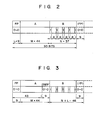
- Fig. 2 shows a format used in the present invention.
- Reference symbol FP denotes a sync signal; and A and B, first and second fields, respectively.
- the first field is formed of one or both of information and check bits.
- the second field is formed of fixed bits and one or both of information and check bits.
- First field A and second field B thus constitute a combination of information bits + check bits + fixed bits.
- Bit length L of sync signal FP has 9 bits, all "0"s.
- Second field B includes end bits, as fixed bits of "1 and information or check bits. One fixed bit of "1 is inserted for every eight bits. The total number of inserted fixed bits is 5.
- Bit length M of field A has 44 bits and bit length N of field B has 37 bits.
- the length of one frame has 90 bits, as in the conventional frame length in Fig. 23.
- Fig. 3 is a code pattern format for explaining an advantage of the format in Fig. 2, showing the case wherein spurious sync signal PFP appears at the end of field A of Fig. 2.
- the spurious sync signal is formed of 9 bits of all "0"s, i.e., the same pattern as signal FP (to be referred to as a sync pattern hereinafter).
- the spurious sync signal is distinguished from signal FP in the following manner.
- Second field B is present immediately before true sync signal FP.
- the sync pattern (nine continuous bits of "0") cannot be produced.
- Fig. 3 shows the relationship between the sync signal of the current frame and the sync signal (FP indicated by the broken line) of the next frame.
- First field A cannot be the same pattern as in the case wherein the sync signal follows second field B. Even if signal PFP appears at a portion excluding the end of field A, the underlined relationship is kept unchanged. Therefore, signal FP can be clearly distinguished from signal PFP.
- Fig. 4 is a block diagram showing an arrangement of a circuit for discriminating the relationship in Fig. 3, i.e., a circuit for detecting true sync signal FP from one-frame data including spurious sync signal PFP.
- the reception code included in decoded signal E28 is stored in shift register 1.
- Content E1 of register 1 is decoded by decoder 2.
- output AFP is generated (i.e., decoder 2 comprises a comparator using the sync pattern as comparison data).
- Code pattern detection by the shift register and the decoder is a conventional technique, and a detailed description thereof will be omitted.
- Output AFP is applied to clear terminal CL of counter 3 so that counter 3 is cleared.
- Counter 3 counts clocks (of the same frequency as that of clock E20 in Fig. 1) synchronized with the reception code.
- Output E4 is delayed by delay element - (D type flip-flop) 5 by one bit. Delayed output E5 is applied to one input terminal of AND gate 6.
- Output AFP is applied to the other input terminal of AND gate 6. Output AFP is produced whether signal E28 includes the true sync signal or whether it includes the spurious sync signal.
- the above circuit extracts sync signal FP from the format in Fig. 2.
- the format in Fig. 2 can be easily created by a conventional technique. However, a method of forming the format of Fig. 2 will be described in detail with reference to Figs. 24 to 26.
- the format in Fig. 2 has the same frame length, i.e., 90 bits, as that of the conventional format in Fig. 23.
- first field A does not require fixed bits so that four bits can be utilized as information bits, thus achieving the prescribed object of an improvement in transmission efficiency.
- transmission efficiency is improved while unique pattern conditions are maintained, thus providing a great practical effect.
- Fig. 5 is a flow chart for discriminating the relationship shown in Fig. 3 by means of software.
- the procedures of a microcomputer constituting frame sync detector 29 of Fig. 1 are shown in Fig. 5.
- a microcomputer fetches the reception code (E28) bit by bit (step SO), and a soft counter (not shown) in the microcomputer is incremented one by one accordingly (step S1).
- step S2 the microcomputer checks whether the bits of the 9-bit reception code E28 are all "0"s. If NO in step S2, the flow ends. However, if YES in step S2, the microcomputer checks the count of counter 3 in step S3.
- the above operations by means of software are the same as those of the hardware in Fig. 4. Thus, software detection of the sync signal - (FP) from the reception code (E28) can be conveniently performed, as shown in Fig. 5.
- Fig. 6 is a format showing a modification of that in Fig. 2. Compared with the format in Fig. 2, the format in Fig. 6 is the same except that first and second fields A and B are reversed.
- Fig. 7 is a code pattern format for explaining an advantage of the format of Fig. 6. More specifically, Fig. 7 explains a pattern discriminated from a pattern wherein second field B follows sync signal FP even if spurious sync signal PFP appears in first field A.
- Fig. 8 is a block diagram of a circuit for discriminating the relationship shown in Fig. 7.
- the arrangement in Fig. 8 is similar to that of Fig. 4, except that in Fig. 8, flip-flop 12 is added, and comparator 13 is used in place of comparator 4 of Fig. 4.
- output AFP is generated from decoder 2 according to the sync pattern included in the reception code - (E28)
- counter 3 is cleared.
- Output AFP is supplied to terminal S of flip-flop 12 so that flip-flop 12 is set and output ASY is output therefrom.
- Output ASY is input to AND gate 6A.
- Fig. 9 is a format showing another modification of that in Fig. 2.
- Fig. 9 only the contents of sync signal FP and the fixed bits of second field B are reversed, compared with those of Fig. 2. More specifically, "1 and "0" are reversed. With such an arrangement, the relationship is kept unchanged.
- Fig. 10 shows a format when the method of the present invention is not used.
- One frame consists of an 8-bit sync signal and other 67 bits, a total of 75 bits.
- the sync signal consists of seven continuous bits of "0" and one bit of "1".
- the fixed bit of "1" is inserted for each information or check bit.
- the sum of information and check bits is a total of 58 bits.
- Fig. 11 shows another format used in the present invention.
- This format has a conspicuous characteristic compared with that in Fig. 10.
- An apparent or spurious sync signal is not produced from field B.
- Fig. 12 is a format showing a modification of that in Fig. 11. Compared with the case in Fig. 11, the positions of fixed bits in second field B are changed. More specifically, at the end of the second field, each fixed bit of "1 is inserted between the three and four information or check bits, and after the three information or check bits. This differs from the case in Fig. 11 wherein the number of information or check bits is six or one. However, a total number of fixed bits in Fig. 12 is equal to that in Fig. 11. The fixed bits are inserted such that the sync pattern is not produced in both Figs. 11 and 12. The same effect as in Fig. 11 can be obtained in Fig. 12.
- Fig. 13 is a format showing a modification of that in Fig. 12.
- the format in Fig. 13 is substantially the same as that in Fig. 12, except that bit assignment at the boundary between sync signal FP1 and second field B1 is different. More specifically, sync signal FP1 consists of one bit of "1 and seven bits of "0" following the one bit of "1 ". No fixed bit is inserted at the end of second field B1. If the last fixed bit "1 " of the second field in Fig. 12 is inserted in the sync signal, the boundary is shifted by one bit. In this sense, the formats in Figs. 12 and 13 are based on an identical concept. Mere modifications such as those shown in Fig. 12 or 13 fall within the scope of the present invention.
- Fig. 14 is a format showing another modification of that in Fig. 12.
- the format in Fig. 14 is substantially the same as that in Fig. 12, except that one fixed bit of "1 " is inserted in first field A. Insertion of the fixed bit is not required in the previous formats. However, in order to indicate a partition boundary between adjacent data strings, the fixed bit is inserted in the first field. In this case, the fixed bit is inserted regardless of length L of the sync signal.
- the characteristic of the bit pattern of first field A is the same as that shown in Fig. 12. Therefore, the modification shown in Fig. 14 can also fall within the scope of the present invention.
- Fig. 15 is a block diagram showing a second embodiment of the present invention, and Figs. 16 to 22 show formats used therein.
- the block diagram in Fig. 15 is substantially the same as that in Fig. 1, except that operations of components 21 A, 23A, 24A and 26A are slightly different from components 21, 23, 24, and 26 in Fig. 1, respectively.
- Sync signal generator 21A generates 8-bit sync signal E21A consisting of seven bits of "0" and one bit of "1" following the seven bits.
- Counter 23A generates output E23A 36 bits after the end of sync signal E21A.
- Fixed bit insertion circuit 24A inserts one fixed bit of "1 immediately after generation of output E23A from counter 23A or for every six information bits.
- Fixed bit insertion circuit 26A generates one fixed bit of "1 for every six bits in the remaining string of information and check bits.
- Other arrangements of Fig. 15 are the same as those of Fig. 1.
- Fig. 16 is a format used in the second embodiment of the present invention.
- One frame consists of 8-bit sync signal FP2, 36-bit first field A, and 31- bit second field B2, a total of 75 bits.
- Signal FP2 is formed of seven bits of "0" and one bit of "1 following the seven bits of "0".
- the bit of "1" in signal FP2 is located at the boundary between fields A and B2.
- Field B2 is similar to that of Fig. 11. However, field B2 in Fig. 16 does not have the same fixed bit of "1" at the end of second field B of Fig. 11. This bit position is assigned to an information or check bit. Even so, a total number of bits of the sync signal and the fixed bits is 13, which is the same as that in Fig. 11.
- the pattern formed of second field B2 and sync signal FP2 does not appear near first field A. Therefore, a synchronization pattern can be detected in the same manner as in the previous embodiment, which will be described in more detail with reference
- Fig. 17 is a code pattern format for explaining the advantage of the format in Fig. 16, particularly when spurious sync signal PFP appears near the end of first field A and the beginning of second field B2.
- Fig. 18 is a format showing a modification of that in Fig. 16.
- the format in Fig. 18 is substantially the same as that in Fig. 16, except that the bit pattern near the end of second field B2 is different. More specifically, the fixed bit of "1" is inserted between one and seven bits in Fig. 18, while the fixed bit of "1" is inserted between six and two bits in Fig. 16. A total number of fixed bits in Fig. 18 is the same as that in Fig. 16. The same effect as the format in Fig. 16 can be obtained in that of Fig. 18. This will be described with reference to Fig. 19.
- Fig. 19 is a code pattern format for explaining the advantage of the format in Fig. 18.
- the format in Fig. 19 is substantially the same as that in Fig. 17, except that the last seven bits of second field B2 are all "0"s.
- the beginning of the sync signal (FP of a broken line) of the next frame is "0".
- Fig. 20 is a format showing a modification of that in Fig. 18.
- the format in Fig. 20 is the same as that in Fig. 18, except that "1 and "0" are reversed.
- Fig. 21 is a format showing a modification of that in Fig. 20.
- the format in Fig. 21 is substantially the same as that in Fig. 20, except that first and second fields A and B2 are reversed.
- the relationship between Figs. 20 and 21 is the same as that between Figs. 2 and 6.
- the same effect as in Fig. 20 can be obtained in Fig. 21.
- Fig. 22 is a format showing a modification of that in Fig. 21.
- the format in Fig. 22 is substantially the same as that in Fig. 21, except that the beginning of second field B2 is the fixed bit of "0".
- the format in Fig. 22 is similar to that in Fig. 14. Even if fixed bits are added for some purpose, the advantage of the present invention is not lost unless fixed bits are inserted at an interval less than a predetermined value throughout the frame. In addition, even if the contents of the sync signal are regarded as "01 -10" including the fixed bit, the boundary between the sync signal and the first or second field . is only subjectively changed. Thus, the scope of the present invention does not change.
- Figs. 24A to 24H show generation timings of signals E20 to E27 in order to cause the arrangement of Fig. 1 to form the bit pattern (format) of Fig. 2.
- Signal E24 in Fig. 24E is generated by fixed bit insertion circuit 24, shown in Fig. 25.
- Signal E26 in Fig. 24G is generated by fixed bit insertion circuit 26 shown in Fig. 26.
- Each bit of the 90-bit, one-frame format in Fig. 2 is defined by clock E20 (Fig. 24A) generated by clock generator 20 in Fig. 1.
- sync signal E21 (Fig. 24B) of nine continuous bits of all "0"s is output from sync signal generator 21.
- Information bit generator 22 generates, from trailing edge (t20) of signal E21, corresponding information bit signal E22 (Fig. 24C) for a period of time to the 65 clocks of E20 - (t40).
- Counter 23 starts counting clocks E20 upon generation (t10) of sync signal E21. When the count of counter 23 reaches 54 (t30), it outputs carrier output E23 (Fig. 24D). Counter 23 is temporarily reset in response to the next sync signal E21, and output E23 is disabled at the start (t50) of E21. Signal E23 representing the duration (t30 to t50) of second field B in one-frame data (t10 to t50) can be obtained.
- the resultant signals E21 to E23 and clock E20 are supplied to insertion circuit 24 in Fig. 25.
- Sync signal E21 and information bit signal E22 are supplied to the first input of OR gate 241.
- Signal E23 is supplied to the D input terminal of D type flip-flop (D.FF) 242.
- D.FF 242 is clocked in response to E20.
- Signal E242, delayed by one clock E20, is output from D.FF 242.
- the inverted logical value of signal E242 and the logical AND of signal E23 are gated by AND gate 243, thereby obtaining signal E243 including fixed bit FBI (Fig. 24E) having a one-clock width of clock E20.
- Signal E243 is supplied to the second input of OR gate 241.
- Signal E23 and clock E20 are input to AND gate 244.
- Clock E20 is gated through gate 244 for a period (t30 to t50 in Fig. 24D) in which signal E23 is kept at logic "1", and serves as counter clock pulse E244.
- Pulse E244 is supplied to clock input CK of modulo 9 ring counter 245.
- Counter 245 outputs carry output E245 corresponding to the fixed bit for every nine pulses.
- Output E245 is supplied to the first input of AND gate 246.
- Pulse E244 is also supplied to clock input CK of modulo 21 counter 247. When counter 247 counts 21 pulses, it outputs carry output E247.
- Signal E23 is supplied to the S input of reset/set flip-flop (RS*FF) 248.
- RS.FF 248 is set at the leading edge of E23 and reset at the leading edge of E247 from counter 247.
- RS*FF 248 outputs gate signal E248 having a duration from the start time (t30 in Fig. 24A) of second field B to 21 st clock (t40 in Fig. 24A).
- Signal E248 is supplied to the second input of AND gate 246.
- Two fixed bits - (FB2 and FB3 in Fig. 24E) pass through gate 246.
- Output E246 in carry output E245 from gate 246 is supplied to the third input of OR gate 241.
- Signal E24 (Fig. 24E) corresonding to the sum of signals E21, E22, E243, and E246, is obtained from OR gate 241.
- Counters 245 and 247 are simultaneously cleared by the trailing edge (t50 in Fig. 24D) of signal E23, and the standby operation for the next frame is thus completed.
- Check bit generator 25 in Fig. 1 generates check bit signal E25 (Fig. 24F) from the trailing edge (t40 in Fig. 24E) of signal E24 within one frame.
- Signal E25, signal E23, and clock E20 are input to insertion circuit 26 in Fig. 26.
- Signal E25 is first supplied to the first input of OR gate 261.
- Signal E23 and clock E20 are input to AND gate 264.
- Modulo 9 ring counter 265 and modulo 21 counter 267 are clocked in response to output E264 from gate 264. Whenever counter 265 counts nine pulses E264, it outputs carry output E265. Whenever counter 267 counts 21 pulses E264, it outputs carry output E267.
- Counter outputs E265 and E267 are input to AND gate 266. Whenever counter 265 counts 9 pulses E264, E265 is input to AND gate 266. However, until counter 267 counts 21 pulses, output E266 from gate 266 is kept at logic "0". When counter 267 counts up 21 pulses E264 (t40 in Fig. 24A) upon opening of gate 264 (t30 in Fig. 24A), E267 becomes logic "1 " so that subsequent pulses E265 after time (t40) pass through gate 266. Signal E266 output from gate 266 becomes signal E266 including fixed bits (FB4 and FB5 in Fig. 24G) to be inserted in check bit signal E25 in second field B. Signal E266 is supplied to the second input of OR gate 261, and signal E266 (Fig. 24g), corresponding to signal E25 + E266, is output from gate 261.
- Counters 265 and 267 are simultaneously cleared at the trailing edge (t50 in Fig. 24D) of signal E23, thereby completing the standby operation for the next frame.
- Fig. 27 is a flow chart for exemplifying how to fetch bit pattern in Fig. 2 or Fig. 24H in a microcomputer when frame data having this bit pattern is processed using the microcomputer.
- the microcomputer first fetches 9-bit sync signal (t10 to t20 in Fig. 24B) (ST10).
- the microcomputer then fetches 44 information bits in first field A (t20 to t30 in Fig. 24C; ST12) and clears content N of an index counter (not shown) (ST14).
- the microcomputer fetches the first fixed bit (FB1 in Fig. 24E) in second field B (ST16) and then the following eight information bits (ST18).
- the microcomputer fetches the third fixed bit - (FB3) of second field B (ST24) and then two information bits (ST26).
- the micorcomputer then sequentially fetches six check bits (ST28), the fourth fixed bit (FB4) (ST30), eight check bits (ST32), and the fifth fixed bit (FB5) (ST34), thereby finishing fetching of the one-frame data pattern.
- Fig. 28 shows a modification of the flow chart in Fig. 27.
- This modification shows a flow chart of other procedures for performing the same operations as in Fig. 27.
- Steps ST40 to ST44 in Fig. 28 are identical with steps ST10 to ST14, while the steps after step ST46 are different from those in Fig. 27.
- the microcomputer fetches the first fixed bit FB1 in second field B (ST46) and increments content N of an index counter (not shown) by one - (ST48).
- Fig. 29 is a flow chart for exemplifying how to cause a microcomputer to fetch the pattern of Fig. 6 when frame data having the bit pattern in Fig. 6 is processed using the microcomputer.
- the microcomputer fetches the 9-bit sync signal (ST60).
- Content N of an index counter (not shown) is cleared (ST62). Subsequently, one fixed bit is fetched (ST64), and eight information bits in first field A are then fetched (ST66).
- N of the index counter is incremented by one (ST68).
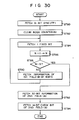
- Fig. 30 is a modification of the flow chart in Fig. 29, and shows a flow chart for other procedures for fetching the bit pattern of Fig. 6.
- Steps ST80 to 84 in Fig. 30 are the same as ST60 to ST64 in Fig. 29.
- Step ST86 and subsequent steps in Fig. 30 are different from those in Fig. 29.
- the loop of ST84 to ST90 is repeated five times (YES at ST88)
- 30 information bits in second field A are fetched (ST92) and 14 check bits are fetched (ST94), thereby completing the fetching of the one-frame data pattern.
- the fixed bit can be "1" or "0".
- the numbers of information and check bits can be arbitrarily selected.
- the fetch timings of sync signals (FP) in the first steps - (ST10, ST40, ST60, and ST80) in Figs. 27 to 30 can be determined by using the software of Fig. 5 or the hardware of Fig. 4 or 8.
- the fixed bits are inserted in only half of one frame so that a sync pattern does not appear in the half containing the fixed bits.
- the pattern formed of the interval in which the sync pattern does not appear and of the sync signal is used for the remaining half of the frame.
- the portion in which the fixed bits need not be inserted is about 1/2 of one frame. Therefore, transmission efficiency can be improved compared with the method using the pattern in Fig. 10 or 23.
Landscapes
- Engineering & Computer Science (AREA)
- Computer Networks & Wireless Communication (AREA)
- Signal Processing (AREA)
- Physics & Mathematics (AREA)
- Spectroscopy & Molecular Physics (AREA)
- Synchronisation In Digital Transmission Systems (AREA)
- Time-Division Multiplex Systems (AREA)
Applications Claiming Priority (2)
| Application Number | Priority Date | Filing Date | Title |
|---|---|---|---|
| JP60166794A JPS6229239A (ja) | 1985-07-30 | 1985-07-30 | サイクリツク情報伝送装置におけるフレ−ム同期方式 |
| JP166794/85 | 1985-07-30 |
Publications (2)
| Publication Number | Publication Date |
|---|---|
| EP0216066A2 true EP0216066A2 (de) | 1987-04-01 |
| EP0216066A3 EP0216066A3 (de) | 1989-01-18 |
Family
ID=15837796
Family Applications (1)
| Application Number | Title | Priority Date | Filing Date |
|---|---|---|---|
| EP86110157A Withdrawn EP0216066A3 (de) | 1985-07-30 | 1986-07-23 | Synchronisiersystem für digitale Informationsübertragung |
Country Status (5)
| Country | Link |
|---|---|
| US (1) | US4809305A (de) |
| EP (1) | EP0216066A3 (de) |
| JP (1) | JPS6229239A (de) |
| KR (1) | KR910000695B1 (de) |
| CN (1) | CN1004043B (de) |
Cited By (3)
| Publication number | Priority date | Publication date | Assignee | Title |
|---|---|---|---|---|
| EP0848517A1 (de) * | 1996-12-13 | 1998-06-17 | Alcatel | Datenübertragungsrahmen und Verfahren und Einrichtung, um einen solchen Rahmen zu senden oder zu empfangen |
| EP0720318A3 (de) * | 1994-12-27 | 1999-04-28 | Nec Corporation | Zeitmultiplexsender und Dekodierschaltung für Multiplexübertragung |
| KR100442926B1 (ko) * | 1999-05-17 | 2004-08-02 | 루센트 테크놀러지스 인크 | 데이터 인코딩 방법 및 장치와 인코딩 데이터 신호의 디코딩 방법 및 장치 |
Families Citing this family (5)
| Publication number | Priority date | Publication date | Assignee | Title |
|---|---|---|---|---|
| JPS6376623A (ja) * | 1986-09-19 | 1988-04-06 | Mitsubishi Electric Corp | Crc生成回路 |
| US4991004A (en) * | 1988-02-05 | 1991-02-05 | Fuji Photo Film Co., Ltd. | Film previewer which simultaneously displays a 110 and a 135 frame |
| US5511099A (en) * | 1994-03-30 | 1996-04-23 | Samsung Electronics Co., Ltd. | Passband sync block recovery |
| KR0185918B1 (ko) * | 1995-02-27 | 1999-04-15 | 김광호 | 동기신호 오류정정을 통한 데이타의 s/p변환방법 및 장치 |
| US6856660B1 (en) * | 1996-10-11 | 2005-02-15 | Hitachi, Ltd. | Signal processing method and apparatus and disk device using the method and apparatus |
Family Cites Families (5)
| Publication number | Priority date | Publication date | Assignee | Title |
|---|---|---|---|---|
| JPS5635059A (en) * | 1979-08-31 | 1981-04-07 | Toshiba Corp | Measuring method of cr-mo-v system heat resistant steel |
| US4503490A (en) * | 1981-06-10 | 1985-03-05 | At&T Bell Laboratories | Distributed timing system |
| US4484327A (en) * | 1983-05-02 | 1984-11-20 | The United States Of America As Represented By The Secretary Of The Army | Pulse code modulation rate converter |
| US4519073A (en) * | 1983-06-20 | 1985-05-21 | At&T Bell Laboratories | Bit compression multiplexer |
| CA1232693A (en) * | 1985-09-05 | 1988-02-09 | Alan F. Graves | Network multiplex structure |
-
1985
- 1985-07-30 JP JP60166794A patent/JPS6229239A/ja active Granted
-
1986
- 1986-07-18 US US06/886,894 patent/US4809305A/en not_active Expired - Lifetime
- 1986-07-23 EP EP86110157A patent/EP0216066A3/de not_active Withdrawn
- 1986-07-25 KR KR1019860006091A patent/KR910000695B1/ko not_active Expired
- 1986-07-30 CN CN86105554.3A patent/CN1004043B/zh not_active Expired
Cited By (4)
| Publication number | Priority date | Publication date | Assignee | Title |
|---|---|---|---|---|
| EP0720318A3 (de) * | 1994-12-27 | 1999-04-28 | Nec Corporation | Zeitmultiplexsender und Dekodierschaltung für Multiplexübertragung |
| EP0848517A1 (de) * | 1996-12-13 | 1998-06-17 | Alcatel | Datenübertragungsrahmen und Verfahren und Einrichtung, um einen solchen Rahmen zu senden oder zu empfangen |
| EP1445882A3 (de) * | 1996-12-13 | 2005-05-04 | Alcatel | Datenübertragungsrahmen und Verfahren und Einrichtung, um einen solchen Rahmen zu senden oder zu empfangen |
| KR100442926B1 (ko) * | 1999-05-17 | 2004-08-02 | 루센트 테크놀러지스 인크 | 데이터 인코딩 방법 및 장치와 인코딩 데이터 신호의 디코딩 방법 및 장치 |
Also Published As
| Publication number | Publication date |
|---|---|
| EP0216066A3 (de) | 1989-01-18 |
| KR870001716A (ko) | 1987-03-17 |
| KR910000695B1 (ko) | 1991-01-31 |
| US4809305A (en) | 1989-02-28 |
| CN1004043B (zh) | 1989-04-26 |
| JPS6229239A (ja) | 1987-02-07 |
| CN86105554A (zh) | 1987-04-22 |
| JPH0457261B2 (de) | 1992-09-11 |
Similar Documents
| Publication | Publication Date | Title |
|---|---|---|
| CA1202435A (en) | Synchronization system for multiplexed digital packets | |
| JPH055711Y2 (de) | ||
| US4404675A (en) | Frame detection and synchronization system for high speed digital transmission systems | |
| CA1212161A (en) | Ring communications system | |
| US4809305A (en) | Cyclic digital information transmission system | |
| EP0393952B1 (de) | Einrichtung und Verfahren zur richtigen Dekodierung in einem Kodierer/Dekodierer | |
| EP0326614B1 (de) | Synchrone signaldekodiervorrichtung | |
| EP0368537B1 (de) | Zuverlässige Datenrückgewinnung in einem Kodierer/Dekodierer | |
| CA1120120A (en) | Frame search control for digital transmission system | |
| US5265105A (en) | Decoding circuit for inhibiting error propagation | |
| JPH0149062B2 (de) | ||
| JP3783563B2 (ja) | データ送信方法、送信装置およびデータ受信方法、受信装置 | |
| JPS60235549A (ja) | nB1C符号信号のCビツト同期方式 | |
| JP3110387B2 (ja) | マルチフレーム同期検出装置 | |
| JPH0221183B2 (de) | ||
| JPS5819055A (ja) | クロツク再生回路 | |
| RU1809534C (ru) | Устройство дл исправлени ошибок в волоконно-оптических системах передачи информации | |
| SU1363516A1 (ru) | Стартстопный демодул тор | |
| JPS62147832A (ja) | フレ−ム同期方法 | |
| JPS588782B2 (ja) | マルチフレ−ム同期装置 | |
| JPH05226938A (ja) | 周波数変調符号化データ復調方法及び復調装置 | |
| JPS643101B2 (de) | ||
| JPH10262225A (ja) | アナログ映像信号においてデータを送信するための記号タイミング発生及び回復システム及び方法 | |
| JPS6129228A (ja) | デジタルデ−タ伝送方式 | |
| JPH02226932A (ja) | Cmi符号の受信装置 |
Legal Events
| Date | Code | Title | Description |
|---|---|---|---|
| PUAI | Public reference made under article 153(3) epc to a published international application that has entered the european phase |
Free format text: ORIGINAL CODE: 0009012 |
|
| 17P | Request for examination filed |
Effective date: 19860820 |
|
| AK | Designated contracting states |
Kind code of ref document: A2 Designated state(s): CH DE FR GB LI SE |
|
| PUAL | Search report despatched |
Free format text: ORIGINAL CODE: 0009013 |
|
| AK | Designated contracting states |
Kind code of ref document: A3 Designated state(s): CH DE FR GB LI SE |
|
| 17Q | First examination report despatched |
Effective date: 19910125 |
|
| STAA | Information on the status of an ep patent application or granted ep patent |
Free format text: STATUS: THE APPLICATION IS DEEMED TO BE WITHDRAWN |
|
| 18D | Application deemed to be withdrawn |
Effective date: 19910915 |
|
| RIN1 | Information on inventor provided before grant (corrected) |
Inventor name: YAMAURA, MITSURUC/O PATENT DIVISION |