EP0216305A2 - Appareil pour l'inspection de films - Google Patents
Appareil pour l'inspection de films Download PDFInfo
- Publication number
- EP0216305A2 EP0216305A2 EP86112852A EP86112852A EP0216305A2 EP 0216305 A2 EP0216305 A2 EP 0216305A2 EP 86112852 A EP86112852 A EP 86112852A EP 86112852 A EP86112852 A EP 86112852A EP 0216305 A2 EP0216305 A2 EP 0216305A2
- Authority
- EP
- European Patent Office
- Prior art keywords
- objects
- checking apparatus
- film
- film checking
- white
- Prior art date
- Legal status (The legal status is an assumption and is not a legal conclusion. Google has not performed a legal analysis and makes no representation as to the accuracy of the status listed.)
- Granted
Links
Images




Classifications
-
- G—PHYSICS
- G03—PHOTOGRAPHY; CINEMATOGRAPHY; ANALOGOUS TECHNIQUES USING WAVES OTHER THAN OPTICAL WAVES; ELECTROGRAPHY; HOLOGRAPHY
- G03F—PHOTOMECHANICAL PRODUCTION OF TEXTURED OR PATTERNED SURFACES, e.g. FOR PRINTING, FOR PROCESSING OF SEMICONDUCTOR DEVICES; MATERIALS THEREFOR; ORIGINALS THEREFOR; APPARATUS SPECIALLY ADAPTED THEREFOR
- G03F3/00—Colour separation; Correction of tonal value
- G03F3/10—Checking the colour or tonal value of separation negatives or positives
- G03F3/101—Colour or tonal value checking by non-photographic means or by means other than using non-impact printing methods or duplicating or marking methods covered by B41M5/00
-
- G—PHYSICS
- G03—PHOTOGRAPHY; CINEMATOGRAPHY; ANALOGOUS TECHNIQUES USING WAVES OTHER THAN OPTICAL WAVES; ELECTROGRAPHY; HOLOGRAPHY
- G03F—PHOTOMECHANICAL PRODUCTION OF TEXTURED OR PATTERNED SURFACES, e.g. FOR PRINTING, FOR PROCESSING OF SEMICONDUCTOR DEVICES; MATERIALS THEREFOR; ORIGINALS THEREFOR; APPARATUS SPECIALLY ADAPTED THEREFOR
- G03F9/00—Registration or positioning of originals, masks, frames, photographic sheets or textured or patterned surfaces, e.g. automatically
Definitions
- the present invention relates to a checking apparatus for a master film etc. for a printing plate, and more particularly to a checking apparatus for determining whether or not a new film has errors, by comparing an uncorrected old film and the corrected new film.
- various materials such as a film obtained by subjecting a color picture original film to color separation and a halftone process, a character original formed by a computer type setting device, a tint, and a lightproof mask film are adhered on a transparent film in accordance with a predetermined layout and in units of colors.
- the obtained films are multi-exposed and nega/posi or posi/nega inverted to obtain four master films of yellow (Y), magenta (M), cyan (C), and black (BK).
- Y yellow
- M magenta
- C cyan
- BK black
- the master films are placed on a pre-sensitized plate (PS plate) and the PS plate is exposed to form a printing plate.
- a proof is printed from the printing plate and subjected to client proofreading.
- the master films must be checked and corrected before forming the printing plate and after the proofreading. For example, they must be checked to determine whether the error has been corrected, whether the color separation films are registered among the four color master films, and whether the tint and characters are arranged at predetermined designated positions. The master films may sometimes have to be formed again if there are many errors. Also, the first master films containing errors may be compared with revised master films. In this case, since the master films are formed manually and in complex procedures and the proofreading is a manual work, a portion of a first film other than the defective or designated portion can be erroneously corrected in a second film.
- a hard copy of, e.g., a rough proof is conventional strictlyly prepared for the master film checking. However, it increases running costs such as material costs.
- a transmission-type object i.e., a master film
- a relfection-type object such as a blue print formed from a master film, a photocopy, a proof, and a block copy cannot be photographed.
- a printout sample must be corrected several times during printing, and the printout sample must also be checked several times. Therefore, it is inconvenient if only a transmission-type object, e.g., a master film can be picked up.
- a large space is required for the conventional apparatus since four color films of Y, M, C, and BK are held on a single plane. Since the relative positional precision among the four TV cameras must be high, the apparatus becomes expensive. Since the TV cameras correspond to Y, M, C, and BK, respectively, the master films must be placed at corresponding predetermined positions.
- the white and black levels of the respective TV cameras must be adjusted to be the same. Conventionally, however, a level of an output signal of a TV camera is displayed on an oscilloscope and the white and black levels are adjusted while monitoring the oscilloscope screen. Therefore, adjustment operation is complex, and a space for an oscilloscope is needed.
- a film checking apparatus comprises transparent tables for respectively placing a plurality of objects thereon, TV cameras for respectively picking up the objects on the tables, a monitor for superposing output images from the TV camera and for displaying the superposed image, a first light source, provided under the tables, for illuminating the objects, a second light source, provided above the tables, for illuminating the objects, and a switch for switching between the first and second light sources in accordance with whether the objects are transmission-type objects or reflection-type objects.
- a film checking apparatus according to an embodiment of the present invention will be described with reference to the accompanying drawings.
- two objects are compared for checking.
- the object include a reflection-type object (a blue print, a photocopy, a proof, a printing plate, and a block copy which are formed from a master film), as well as a transmission-type object (master film).
- Image pickup unit l0 has camera housing 22 incorporating TV cameras used to picking up two objects l8 and 20 placed on film tabels l4 and l6, respectively.
- Film tabels l4 and l6 are formed of a transparent material, such as a glass plate.
- Objects l8 and 20 are positioned on film tables l4 and l6 with register pins 24 and 26.
- As the positioning method a punch system method, a method wherein reference lines are drawn on tables l4 and l6 and objects are aligned thereto, and so on are available. Since objects l8 and 20 placed on tables l4 and l6 may be curled, a means for holding them flat is also required.
- vacuum holes can be formed in tables l4 and l6, and the objects can be drawn by a vacuum pump through the vacuum holes.
- objects can be placed on tables l4 and l6 and thereafter a transparent glass plate can be placed thereon.
- Display unit l2 has color monitor 40 and electric circuit unit 42.
- Fig. 2 is a sectional view of image pickup unit l0.
- TV cameras 50 and 52 are provided in housing 22. The relative positional relationship of cameras 50 and 52 can be adjusted.
- two types of light sources are provided for image-picking up; one for irradiating a transmission-type object, and the other for irradiating a reflection-type object.
- Lamps 54 and 56 are provided under tables l4 and l6 as light sources for irradiating the transmission-type object.
- a DC stabilized power source (not shown) is connected to lamps 54 and 56.
- Lamps 58 and 60 are provided in housing 22 as a light source for irradiating the reflection-type object.
- a DC stabilized power source (not shown) is connected to lamps 58 and 60.
- the light emitted by lamps 58 and 60 is reflected by mirrors 62 and 64 and irradiates objects l8 and 20 on tables l4 and l6.
- Light is reflected by mirrors 62 and 64 in order to increase the optical path length and hence to obtain light of uniform intensity.
- the housing 22 is made compact.
- Cameras 50 and 52 have two interchangeable lenses 66 (67) and 68 (69), respectively.
- the magnifications of the pickup images can be switched between a low magnification (about ⁇ 2.5) and a high magnification (about ⁇ l3).
- Lenses 66 and 68 set the low magnification.
- Lenses 67 and 69 set the high magnification. Magnification is switched since an object must be enlarged when a halftone check is performed.
- Interchangeable lenses can be replaced by zoom lenses.
- Color filters 70 and 72 can be attached on the front faces of lenses 66 (67) and 68 (69) in order to pick up a bright object having a narrow density range, such as a blue print or printing plate.
- filters 70 and 72 are of complementary colors with the colors of the objects.
- a Y-type filter is preferably attached on the front face of a TV camera photographing a blue print
- an R-type filter is preferably attached on the front face of a TV camera photographing a PS plate.
- a centering mechanism for finely adjusting the scope of view in the x- and y-directions is provided to at least one the TV cameras, e.g., TV camera 50, so that the position of camera 50 relative to camera 52 can be finely adjusted.
- This fine adjustment centering mechanism adjusts the relative position between cameras 50 and 52.
- the two master films can then be precisely superposed and displayed on color monitor 40.
- Operation panel 74 and switch box 78 are provided on the front face and on housing 22, respectively.
- Switch box 78 has light source select switches 80 and 82, and shift switches 84 and 86.
- switches 80 and 82 select a light source for irradiating a transmission-type object or a light source for irradiating a reflection-type object.
- Switches 84 and 86 move one of cameras 50 and 52 in the x- and y-directions. When switches 84 and 86 are rotated, one of cameras 50 and 52 is shifted in the x- and y- directions to allow checking of a reflection-type object, unlike the above-described fine adjustment of the scope of view to be photographed.
- a reflection-type object such as a blue print
- its size may thus become slightly different from the master film.
- switches 84 and 86 are operated to move one of the TV cameras. Checking is performed after the two images are correctly aligned with each other.
- one of cameras 50 and 52 is moved only when at least one of the light sources selected by selection switches 80 and 82 is a light source for irradiating a reflection-type object. Cameras 50 and 52 are not moved when both of the light sources are light sources for a transmission-type object. The positions of cameras 50 and 52 are adjusted only by the fine adjustment mechanism described above.
- magnification can be finely changed by changing the scan rate of camera.
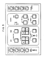
- Fig. 3 is a plan view of operation panel 74.
- White-and black-level controls for the right and left cameras, and a switch for turning on/off the operation of the level display circuit shown in Fig. 4 are located at the leftmost portion of panel 74; nega/posi inversion switches, color selection switches, and flap check switches for the right and left cameras are located on the right side thereof; a white or black blinking designation switch, a blinking level switch, switches for changing pickup magnifications of the cameras between high and low magnifications, and brake switches are located on the right side thereof; and horizontal and vertical centering controls for both high and low magnifications are located at the rightmost portion of panel 74.
- magnification change switches also serve as the light source switches.
- high or low magnification switch When high or low magnification switch is depressed, the light source is turned on; when both high and low magnification switches are depressed, the light source is turned off.
- the low magnification corresponds to ⁇ 2.5 and the high magnification corresponds to ⁇ l3.
- the nega/posi switches invert the image of the object from nega to posi or vice versa in units of the right and left cameras.
- the color selection switches designate the color to be displayed on color monitor 40, i.e., to display images in Y, M, C, BK, R (when switches Y and M are simultaneously depressed), G (when switches Y and C are simultaneously depressed), and B (when switches C and M are simultaneously depressed), in units of the right and left cameras.
- the white background switch also serves as a flap check switch. The white background switch removes the images from the right and left cameras displayed on monitor 40 independently to display white. When flap is designated and one or both of the right and left flap check switches are depressed, the image from one camera is fixed while the image from the other camera is displayed alternately with white background, or the images of the both cameras are displayed alternately.
- the blinking designation switch blinks different portions of display images from the right and left cameras in white, black or any arbitrary color.
- the centering switches are electrical centering controls and can perform centering adjustment in low and high magnifications separately.
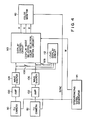
- Fig. 4 is a circuit diagram of electric circuit unit 42 in dispslay unit l2.
- Image signals from TV cameras 50 and 52 are supplied to display control circuit ll0 through amplifier l00 and wave shaper l04, and through amplifier l02 and wave shaper l06, respectively.
- Circuit ll0 processes these image signals and supplies the same to color monitor 40 as R, G, and B color component signals.
- the signals output from wave shapers l04 and l06 are also supplied to level display circuit ll2.
- Outputs from circuit ll2 are added to outputs from wave shapers l04 and l06 through switches l08 and l09.
- Synchronizing signal generator ll4 is provided to supply sync. signals to cameras 50 and 52 and to monitor 40.
- Generator ll4 also generates a pseudo white signal supplied to circuit ll0.
- the pseudo white signal is obtained by adjusting the blanking signal in the sync. signal to white level.
- Fig. 5 is a circuit diagram showing in detail display control circuit ll0 shown in Fig. 4.
- the signals from wave shapers l04 and l06 are supplied to the first input terminals of flap check switches l20 and l22.
- the pseudo white signal is supplied to the second input terminals of switches l20 and l22.
- Output signals from switches l20 and l22 are supplied to matrix circuit l30 through color selection switches l26 and l28 each for coloring the image with Y, M, C, and BK.
- Matrix circuit l30 also receives the pseudo white signal through color selection switch l32 for Y, M, C, and BK.
- R, G, and B signals output from circuit l30 are supplied to color monitor 40 through adders l34, l36, and l38.
- the signals from wave shapers l04 and l06 are also supplied to subtracter l40 to obtain a difference therebetween.
- a signal output from subtracter l40 is supplied to the first input terminal of comparator l42 and is compared with reference level signal Vth which is supplied to the second input terminal thereof.
- Vth reference level signal
- comparator l42 supplies an output signal of level "l" to the first input terminal of AND gate l46.
- the second input terminal of AND gate l46 receives clock pulse CK which determines the blinking period.
- the period of pulse CK is set at 0.2 second.
- the output signal of gate l46 is supplied to variable resistors l60, l62, and l64 through switch l50 or a combination of switch l52 and inverter l54.
- the signal supplied to resistor l56 is branched to three paths, supplied to mixers l34, l36, and l38 through variable resistors l60, l62, and l64, and added to R, G, and B signals output from circuit l30.
- the circuit ll2 has two channels which respectively receives the outputs of wave shapers l04 and l06.
- Fig. 6 is a circuit diagram showing in detail one channel of the circuit ll2.
- the signal from wave shaper l04 (or l06) is supplied to DC level detector l72.
- Black and white level signals are separated by detector l72 are supplied to black and white level display circuits l76 and l74, respectively.
- the white level signal supplied to circuit l74 is input to the anode of diode l84a through amplifier l80a and gate l82a.
- the cathode of diode l84a is grounded through capacitor l86a.
- the cathode of diode l84a is also connected to one end of each of switches l88a and l90a.
- the other end of each of switches l88a and l90a is connected to each other through capacitor l92a.
- the other end of switch l90a is also grounded.
- the other end of switch l88a is also connected to the (-) input terminal of comparator l94a.
- the (+) input terminal of comparator l94a receives a sawtooth reference signal synchronized with a horizontal blanking signal.
- the output signal of comparator l94a is supplied to the first input terminal of mixer 200 through a differentiator comprising capacitor l96a and resistor l98a.
- Black level display circuit l76 has almost the same configuration as white level display circuit l74.
- the same reference numerals of circuit l76 denote the equivalent circuit element as in circuit l74, with suffix b instead of a .
- diode l84b is connected in the opposite direction to diode l84a of circuit l74, and the output of gate l82b is connected to the cathode of diode l84b.
- the output of circuit l76 is supplied to the second input terminal of mixer 200.
- DC signal Vdc as a reference white level is supplied to the (-) input terminal of comparator 202.
- the (+) input terminal of comparator 202 receives the sawtooth reference signal which is supplied to the (+) input terminals to comparators l94a and l94b.
- Mixer 200 also receives the output signal of comparator 202 through a differentiator comprising capacitor 204 and resistor 206 at its third input terminal. The output of mixer 200 is added to the output from wave shapers l04 or l06 through switches l08 or l09.
- Two master films are placed on film tables l4 and l6.
- Light sources for a transmission-type object are selected with left and right cameras 50 and 52 by selection switches 80 and 82.
- the master films irradiated by lamps 54 and 56 from below are picked up by cameras 50 and 52.
- Color selection switches l26, l28, and l32 on operation panel 74 are operated so that the image signal from camera 50 is supplied to the Y input of matrix circuit l30, the image signal from camera 52 is supplied to the M input of circuit l30, and the pseudo white signal is supplied to the C and BK inputs of circuit l30. Then, a synthesized image having the image from camera 50 in Y and the image from camera 52 in M is displayed on monitor 40.
- Y and M master films are placed on tables l4 and l6, respectively.
- Switches l26, l28, and l32 on panel 74 are operated so that the image signal from camera 50, the image signal from camera 52, and the pseudo white signal are supplied to the Y, M, and C and BK inputs, respectively, of circuit l30.
- a synthesized image comprising an image from camera 50 in Y and that from camera 52 in M is displayed on monitor 40.
- the Y and M master films are removed and C and BK master films are placed on tabels l4 and l6, respectively.
- Switches l26, l28, and l32 on panel 74 are operated so that the image signal from camera 50, the image signal from camera 52, and the pseudo white signal are supplied to the C, BK, and Y and M inputs, respectively, of circuit l30. Then, a synthesized image comprising the image from camera 50 in C and the image from camera 52 in BK is displayed on monitor 40.
- switches l26, l28, and l32 of panel 74 are operated so that the image signal from camera 50 or 52 is simultaneously supplied to the Y and C inputs of circuit l30. Then, an image can be displayed in green on monitor 40.
- the image signals therefrom are in phase.
- the image signal from camera 50, the image signal from camera 52, and the pseudo white signal are supplied to the Y, M, and C and BK inputs, repectively, of circuit l30.
- a synthesized image comprising the image from camera 50 in Y and the image from camera 52 in M is displayed on monitor 40.
- the image signals from cameras 50 and 52 are supplied to subtracter l40 through wave shapers l04 and l06, respectively, and a difference therebetween is calculated.
- the difference signal is compared with reference level signal Vth by comparator l42.
- the different portion between the two master films is displayed by black level blinking to stand out on the display screen.
- the black or white level blinking can be switched by changing the blinking switch on panel 74 shown in Fig. 3 to the black or white side.
- the blinking switch is turned off, both switches l50 and l52 (Fig. 5) are opened, and no blinking is performed.
- the clock pulse supplied to AND gate l46 rises or falls at an arbitrarily time and blinking is thus started midway during a one-frame display. In this case, noise occurs on the screen of color monitor 40.
- the clock pulse is synchronized with a vertical blanking signal so that it rises during a vertical blanking period.
- Flap check is conventionally performed by manual operation. Namely, an operation wherein two master films are superposed, the upper film is peeled and returned, is performed repeatedly in a flap manner in order to detect a difference between the two master films. In the present invention, this flap check is performed on the screen of monitor 40 by electrical signal processing.
- an image signal from at least one TV camera and a pseudo white signal are cyclically, alternately switched and supplied to matrix circuit 130.
- at least one of switches 120 and 122 is switched by a timing signal (having a period of about 0.5 to 2.0 second) from a timer circuit (not shown). Switching is performed during the vertical blanking period in order to prevent noise.
- switch l20 is kept connected to the output side of wave shaper l04 and switch l22 is cyclically switched to the output side of wave shaper l06 and the pseudo white signal side. Then, an image from camera 50 is displayed on monitor 40 and the image from camera 52 is alternately superposed thereon and eliminated therefrom.
- switch l22 is kept connected to the output side of wave shaper l06 and switch l20 is cyclically switched to the output side of wave shaper l04 and the pseudo white signal side. Then, an image from camera 52 is displayed on monitor 40 and the image from camera 50 is alternately superposed thereon and eliminated therefrom.
- switch l20 is cyclically switched to the output side of wave shaper l04 and the pseudo white signal side
- switch l22 is cyclically switched to the pseudo white signal side and the output side of wave shaper l06 in an opposite manner. Then, the images from cameras 50 and 52 are alternately displayed on monitor 40, thereby allowing flap check.
- the images from the respective cameras can be colored arbitrarily in accordance with color selection switches l26, l28, and l32. Flap selection is performed by depressing the right flap switch, the left flap switch, and the both right and left flap switches on panel 74 shown in Fig. 3.
- the image displayed alternately with the image from one of the cameras need not be in white, but can be colored in pale blue so as to prevent fatigue of operator's eyes.
- the pale blue signal may be supplied to switches l20 and l22 in place of the pseudo white signal.
- black and white reference lines Rbk and Rw and actual black and white level lines Lbk and Lw of the image signals from TV camera 50 or 52 are displayed on the screen of monitor 40, as shown in Fig. 7.
- the gain of amplifier l00 or l02 are adjusted to move lines Lbk and Lw to lines Rbk and Rw, thereby performing level adjustment of the image signal from the TV camera.
- a signal Vdc of a DC level corresponding to the white level is supplied to the non-inverting terminal of comparator 202.
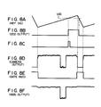
- the inverting terminal of comparator 202 receives the sawtooth reference voltage linearly changing from black to white level in l-H period, as shown in Fig. 8A.
- the signal Vdc of the DC level is compared with the reference voltage.
- the DC level Vdc is indicated by a broken line in Fig. 8A.
- comparator 202 When the sawtooth reference signal exceeds the DC level Vdc, comparator 202 generates an output of level "l", as shown in Fig. 8B. This "l"-level output is differentiated by a differentiator comprising capacitor 204 and resistor 206.
- Black level reference line Rbk fits in the central disconnected portion of line Rw. Therefore, as shown in Figs. 9A and 9B, a gate signal is supplied to gate l82a during a central portion of one field period, e.g., l0 H, and clears the white level reference pulse (differentiation pulse from capacitor 204 and resistor 206). During this period of time, a line Rbk is vertically displayed on the screen of monitor 40 at a transversely shifted position corresponding to the level of the gate signal to gate l82a. Therefore, when the level of the gate signal is set to match the black reference level, line Rbk is displayed to fit in the central portion of line Rw, as shown in Fig. 7.
- a gate signal is supplied to gate l82a during a central portion of one field period, e.g., l0 H, and clears the white level reference pulse (differentiation pulse from capacitor 204 and resistor 206).
- a white level image signal is supplied to the anode of diode l84a.
- This signal passes through gate l82a without being changed during a period excluding the period of the gate pulse shown in Fig. 9B, and is charged on capacitor l86a. Then, a voltage corresponding to the highest white level of the image signal from the TV camera is generated across the terminals of capacitor l86a.
- switch l88a is closed by a charge transfer signal generated at the beginning of the horizontal blanking period, as shown in Fig. l0B
- the signal is transferred to capacitor l92a.
- switch l90a is closed by a discharge signal generated next to the charge transfer signal during the horizontal blanking period, as shown in Fig. l0C, the terminal voltage of capacitor l86a is discharged.
- a voltage corresponding to the highest white level of the image signal of every horizontal scanning line is applied across the terminals of capacitor l92a.
- This voltage is compared with the sawtooth reference signal shown in Fig. 8A by comparator l94a, and white level line Lw is displayed at a position corresponding to the terminal voltage of capacitor l92a.
- line Lw is shifted to the right; when the terminal voltage of capacitor l92a is decreased, line Lw is shifted to the left. Therefore, the position of actual white level line Lw is moved close to reference line Rw by adjusting the gain of amplifier l00 or l02 while monitoring the monitor 40, thereby performing level adjustment.
- This sum signal is charged on capacitor l86b through diode l84b. Then, a voltage corresponding to the lowest black level image signal from the TV cameras is generated across the terminals of capacitor l86b. This voltage is transferred to capacitor l92b by closing switch l88b by a charge transfer signal generated at the beginning of the horizontal blanking period, as shown in Fig. l0B. After this transfer, switch l90b is closed by a discharge signal generated next to the charge transfer signal within the horizontal blanking period, as shown in Fig. l0C, in order to discharge the terminal voltage of capacitor l86b.
- a voltage corresponding to the lowest black level image signal of every horizontal scan line is applied across the terminals of capacitor l92b.
- This voltage is compared with the sawtooth reference signal, shown in Fig. 8A, by comparator l94b, and black level line Lbk is displayed at a position corresponding to the terminal voltage of capacitor l92b.
- the terminal voltage of capacitor l92b is increased, the position of line Lbk is shifted to the right; when the terminal voltage of capacitor l92b is decreased, the position of line Lbk is shifted to the left. Therefore, when the gain of amplifier l00 or l02 is adjusted to move actual black level line Lbk close to reference line Rbk while monitoring the screen, level adjustment can be performed.
- a reflection-type object such as a blue print, a photocopy, a proof, and a printing plate
- a transmission-type object such as a master film
- the master films can be checked by comparison with reflection-type object. It can be easily checked whether the registration between the respective master films is good, whether a character or tint is arranged as designated on the respective master films, and whether a portion to be changed is corrected as designated.
- an inexpensive, small film checking apparatus can be provided.
- level adjustment of a TV camera is facilitated.
Landscapes
- Physics & Mathematics (AREA)
- General Physics & Mathematics (AREA)
- Preparing Plates And Mask In Photomechanical Process (AREA)
- Closed-Circuit Television Systems (AREA)
Applications Claiming Priority (2)
| Application Number | Priority Date | Filing Date | Title |
|---|---|---|---|
| JP213549/85 | 1985-09-26 | ||
| JP60213549A JPS6273263A (ja) | 1985-09-26 | 1985-09-26 | 透過、反射両用検版装置 |
Publications (3)
| Publication Number | Publication Date |
|---|---|
| EP0216305A2 true EP0216305A2 (fr) | 1987-04-01 |
| EP0216305A3 EP0216305A3 (en) | 1989-03-29 |
| EP0216305B1 EP0216305B1 (fr) | 1993-04-07 |
Family
ID=16641038
Family Applications (1)
| Application Number | Title | Priority Date | Filing Date |
|---|---|---|---|
| EP86112852A Expired - Lifetime EP0216305B1 (fr) | 1985-09-26 | 1986-09-17 | Appareil pour l'inspection de films |
Country Status (4)
| Country | Link |
|---|---|
| US (1) | US4816903A (fr) |
| EP (1) | EP0216305B1 (fr) |
| JP (1) | JPS6273263A (fr) |
| DE (1) | DE3688227T2 (fr) |
Families Citing this family (11)
| Publication number | Priority date | Publication date | Assignee | Title |
|---|---|---|---|---|
| IL78675A (en) * | 1986-05-02 | 1993-02-21 | Scitex Corp Ltd | Color separation scanner |
| US5239392A (en) * | 1988-05-10 | 1993-08-24 | Minolta Camera Kabushiki Kaisha | Reading apparatus |
| JPH0775385B2 (ja) * | 1989-02-20 | 1995-08-09 | シャープ株式会社 | 読取装置 |
| DE69030714T2 (de) * | 1989-11-20 | 1997-11-27 | Canon Kk | Bildverarbeitungsgerät |
| IL101029A (en) * | 1992-02-20 | 1996-01-19 | Scitex Corp Ltd | Method for identifying elephant type |
| JP3056329B2 (ja) * | 1992-06-19 | 2000-06-26 | 富士写真フイルム株式会社 | 読取原稿有無判別方法および装置 |
| DE19516059A1 (de) * | 1995-05-04 | 1996-11-07 | Mavis Gmbh Machine Vision | Verfahren und Vorrichtung zur Inspektion von Druckplatten, -folien, -filmen oder Filmmontagen |
| US5748344A (en) * | 1995-09-25 | 1998-05-05 | Xerox Corporation | System and method for determining a location and orientation in a black and white digital scanner |
| US5838464A (en) * | 1995-11-02 | 1998-11-17 | Eastman Kodak Company | System and method for scanning images contained on a strip of photosensitive film |
| US6101000A (en) * | 1998-01-30 | 2000-08-08 | Eastman Kodak Company | Photographic processing apparatus and method |
| US7142335B2 (en) * | 2002-07-22 | 2006-11-28 | Eastman Kodak Company | Method and apparatus for transparency scanning with a duplex reflective scanner |
Family Cites Families (14)
| Publication number | Priority date | Publication date | Assignee | Title |
|---|---|---|---|---|
| GB747680A (en) * | 1952-07-17 | 1956-04-11 | Genevoise Instr Physique | Improvements in and relating to an arrangement for projecting in superposition the images of a work piece and of a reference drawing through an outline projector |
| DE2145844A1 (de) * | 1971-09-14 | 1973-03-22 | Schmalz Siegfried K | Vorrichtung und verfahren zur kontrolle der zur anfertigung von druckstoecken bestimmten farbauszuege eines mehrfarbenbildes |
| US4007326A (en) * | 1976-01-15 | 1977-02-08 | Xerox Corporation | Electronic copy analysis |
| SU652578A1 (ru) * | 1976-07-12 | 1979-03-15 | Предприятие П/Я М-5308 | Устройство дл идентификации цветных изображений |
| DE2939457A1 (de) * | 1979-09-28 | 1981-05-07 | Siemens Ag | Verfahren zur hervorhebung eines bildbereiches innerhalb eines bildes, das auf einem bildschirm dargestellt wird |
| US4310848A (en) * | 1979-10-18 | 1982-01-12 | Carter Equipment Co., Inc. | Colorimetric evaluation of photographic film |
| DE3003607C2 (de) * | 1980-02-01 | 1984-01-05 | Dr.-Ing. Rudolf Hell Gmbh, 2300 Kiel | Schaltungsanordnung zur partiellen Nachkorrektur von Farberkennungsräumen bei der Farberkennung |
| JPS57108854A (en) * | 1980-12-25 | 1982-07-07 | Toppan Printing Co Ltd | Method for checking original plate films and its apparatus |
| JPS5870228A (ja) * | 1981-10-22 | 1983-04-26 | Toppan Printing Co Ltd | フイルム検版装置 |
| JPS5870227A (ja) * | 1981-10-22 | 1983-04-26 | Toppan Printing Co Ltd | フイルム検版装置 |
| JPS58102940A (ja) * | 1981-12-15 | 1983-06-18 | Toppan Printing Co Ltd | フイルム検版装置 |
| JPS58102941A (ja) * | 1981-12-15 | 1983-06-18 | Toppan Printing Co Ltd | フイルム検版装置 |
| JPS61123289A (ja) * | 1984-11-19 | 1986-06-11 | Fuji Photo Film Co Ltd | 写真画像の映像信号記録方法 |
| JPH0733484Y2 (ja) * | 1984-12-17 | 1995-07-31 | シャープ株式会社 | カラー原稿読取装置の光源ユニット |
-
1985
- 1985-09-26 JP JP60213549A patent/JPS6273263A/ja active Granted
-
1986
- 1986-09-17 EP EP86112852A patent/EP0216305B1/fr not_active Expired - Lifetime
- 1986-09-17 DE DE8686112852T patent/DE3688227T2/de not_active Expired - Fee Related
- 1986-09-17 US US06/908,181 patent/US4816903A/en not_active Expired - Fee Related
Also Published As
| Publication number | Publication date |
|---|---|
| EP0216305A3 (en) | 1989-03-29 |
| JPS6273263A (ja) | 1987-04-03 |
| JPH0366654B2 (fr) | 1991-10-18 |
| EP0216305B1 (fr) | 1993-04-07 |
| US4816903A (en) | 1989-03-28 |
| DE3688227D1 (de) | 1993-05-13 |
| DE3688227T2 (de) | 1993-09-23 |
Similar Documents
| Publication | Publication Date | Title |
|---|---|---|
| EP0055939B1 (fr) | Dispositif pour précontempler des copies | |
| US4903068A (en) | Photographic printer | |
| EP0216305A2 (fr) | Appareil pour l'inspection de films | |
| US6873438B2 (en) | Method of image color correction | |
| EP0999440A1 (fr) | Procédé et système pour inspecter des objets | |
| JPS6280662A (ja) | 透過、反射両用検版装置 | |
| JPH0117568B2 (fr) | ||
| JPH0117566B2 (fr) | ||
| JPH0435739B2 (fr) | ||
| JPH0371704B2 (fr) | ||
| JPH0117567B2 (fr) | ||
| JPH0366653B2 (fr) | ||
| JPH02110532A (ja) | シミュレータ付写真プリンタ | |
| JPS63123034A (ja) | カラ−プリンタ | |
| JPH0435740B2 (fr) | ||
| JPH0117569B2 (fr) | ||
| JPH0435741B2 (fr) | ||
| JPH0314668Y2 (fr) | ||
| JPH0366658B2 (fr) | ||
| GB2253319A (en) | Photographic printing apparatus | |
| JPS6273267A (ja) | 透過、反射両用検版装置 | |
| JPS6363900B2 (fr) | ||
| JPS62184446A (ja) | プリンタプロセサ− | |
| JPS6273265A (ja) | 透過、反射両用検版装置 | |
| JPH0677146B2 (ja) | フィルム検版装置 |
Legal Events
| Date | Code | Title | Description |
|---|---|---|---|
| PUAI | Public reference made under article 153(3) epc to a published international application that has entered the european phase |
Free format text: ORIGINAL CODE: 0009012 |
|
| AK | Designated contracting states |
Kind code of ref document: A2 Designated state(s): CH DE FR GB LI |
|
| PUAL | Search report despatched |
Free format text: ORIGINAL CODE: 0009013 |
|
| AK | Designated contracting states |
Kind code of ref document: A3 Designated state(s): CH DE FR GB LI |
|
| 17P | Request for examination filed |
Effective date: 19890609 |
|
| 17Q | First examination report despatched |
Effective date: 19910321 |
|
| GRAA | (expected) grant |
Free format text: ORIGINAL CODE: 0009210 |
|
| AK | Designated contracting states |
Kind code of ref document: B1 Designated state(s): CH DE FR GB LI |
|
| REF | Corresponds to: |
Ref document number: 3688227 Country of ref document: DE Date of ref document: 19930513 |
|
| ET | Fr: translation filed | ||
| PLBE | No opposition filed within time limit |
Free format text: ORIGINAL CODE: 0009261 |
|
| STAA | Information on the status of an ep patent application or granted ep patent |
Free format text: STATUS: NO OPPOSITION FILED WITHIN TIME LIMIT |
|
| 26N | No opposition filed | ||
| PGFP | Annual fee paid to national office [announced via postgrant information from national office to epo] |
Ref country code: GB Payment date: 19960909 Year of fee payment: 11 |
|
| PGFP | Annual fee paid to national office [announced via postgrant information from national office to epo] |
Ref country code: FR Payment date: 19960910 Year of fee payment: 11 |
|
| PGFP | Annual fee paid to national office [announced via postgrant information from national office to epo] |
Ref country code: DE Payment date: 19960920 Year of fee payment: 11 |
|
| PGFP | Annual fee paid to national office [announced via postgrant information from national office to epo] |
Ref country code: CH Payment date: 19961003 Year of fee payment: 11 |
|
| PG25 | Lapsed in a contracting state [announced via postgrant information from national office to epo] |
Ref country code: GB Free format text: LAPSE BECAUSE OF NON-PAYMENT OF DUE FEES Effective date: 19970917 |
|
| PG25 | Lapsed in a contracting state [announced via postgrant information from national office to epo] |
Ref country code: LI Free format text: LAPSE BECAUSE OF NON-PAYMENT OF DUE FEES Effective date: 19970930 Ref country code: FR Free format text: THE PATENT HAS BEEN ANNULLED BY A DECISION OF A NATIONAL AUTHORITY Effective date: 19970930 Ref country code: CH Free format text: LAPSE BECAUSE OF NON-PAYMENT OF DUE FEES Effective date: 19970930 |
|
| GBPC | Gb: european patent ceased through non-payment of renewal fee |
Effective date: 19970917 |
|
| REG | Reference to a national code |
Ref country code: CH Ref legal event code: PL |
|
| PG25 | Lapsed in a contracting state [announced via postgrant information from national office to epo] |
Ref country code: DE Free format text: LAPSE BECAUSE OF NON-PAYMENT OF DUE FEES Effective date: 19980603 |
|
| REG | Reference to a national code |
Ref country code: FR Ref legal event code: ST |