EP0216697A1 - Steuervorrichtung für einen Ausgangskreis einer integrierten Schaltung - Google Patents
Steuervorrichtung für einen Ausgangskreis einer integrierten Schaltung Download PDFInfo
- Publication number
- EP0216697A1 EP0216697A1 EP86402009A EP86402009A EP0216697A1 EP 0216697 A1 EP0216697 A1 EP 0216697A1 EP 86402009 A EP86402009 A EP 86402009A EP 86402009 A EP86402009 A EP 86402009A EP 0216697 A1 EP0216697 A1 EP 0216697A1
- Authority
- EP
- European Patent Office
- Prior art keywords
- transistor
- vcc
- voltage
- base
- circuit
- Prior art date
- Legal status (The legal status is an assumption and is not a legal conclusion. Google has not performed a legal analysis and makes no representation as to the accuracy of the status listed.)
- Granted
Links
Images


Classifications
-
- H—ELECTRICITY
- H03—ELECTRONIC CIRCUITRY
- H03F—AMPLIFIERS
- H03F1/00—Details of amplifiers with only discharge tubes, only semiconductor devices or only unspecified devices as amplifying elements
- H03F1/02—Modifications of amplifiers to raise the efficiency, e.g. gliding Class A stages, use of an auxiliary oscillation
- H03F1/0205—Modifications of amplifiers to raise the efficiency, e.g. gliding Class A stages, use of an auxiliary oscillation in transistor amplifiers
- H03F1/0211—Modifications of amplifiers to raise the efficiency, e.g. gliding Class A stages, use of an auxiliary oscillation in transistor amplifiers with control of the supply voltage or current
- H03F1/0216—Continuous control
- H03F1/0233—Continuous control by using a signal derived from the output signal, e.g. bootstrapping the voltage supply
- H03F1/0238—Continuous control by using a signal derived from the output signal, e.g. bootstrapping the voltage supply using supply converters
-
- H—ELECTRICITY
- H03—ELECTRONIC CIRCUITRY
- H03F—AMPLIFIERS
- H03F3/00—Amplifiers with only discharge tubes or only semiconductor devices as amplifying elements
- H03F3/34—DC amplifiers in which all stages are DC-coupled
- H03F3/343—DC amplifiers in which all stages are DC-coupled with semiconductor devices only
- H03F3/3432—DC amplifiers in which all stages are DC-coupled with semiconductor devices only with bipolar transistors
- H03F3/3435—DC amplifiers in which all stages are DC-coupled with semiconductor devices only with bipolar transistors using Darlington amplifiers
- H03F3/3437—DC amplifiers in which all stages are DC-coupled with semiconductor devices only with bipolar transistors using Darlington amplifiers with complementary transistors
Definitions
- the present invention relates to a control circuit making it possible to reduce this consumption.
- Darlington-type circuits are shown in Figure 1 in several of their possible configurations.
- a general characteristic of Darlington circuits is that they include at least two bipolar transistors and that the gain of the overall circuit is the product of the gains of each of the transistors.
- the Darlington circuit consists of a main transistor T1 of the NPN type and of a control transistor T2 of the PNP type.
- the collector of transistor Tl is connected to the supply voltage and its emitter to ground via a load 10.
- the base of transistor Tl is connected to the collector of transistor T2 whose emitter is connected to voltage VCC power supply.
- the control signal is applied to the base of the transistor T2 and is symbolized by a current source IB2 connected between this base and the ground.
- the Darlington circuit comprises two bipolar transistors of PNP type T1 and T2.
- the emitter of the main transistor Tl is connected to the supply voltage VCC and the collector of the transistor Tl is grounded via a load 10.
- the base of the transistor Tl is connected to the emitter of the transistor T2 control whose collector is connected to the collector of the transistor T1.
- the base of the transistor T2 receives the control signal shown diagrammatically in the form of a current source IB2 connected between this base and the ground.
- FIG. 1C a Darlington circuit is shown in which the two transistors are of the NPN type.
- the collector of transistor Tl is connected to the collector of transistor T2, these two collectors being connected to the supply voltage VCC by via a load 12.
- the emitter of transistor Tl is connected to ground and its base to the emitter of transistor T2.
- the base of transistor T2 receives the control signal symbolized by a current source IB2 connected between the supply voltage VCC and this base.
- a Darlington circuit can be generally defined as a bipolar circuit comprising a first main transistor Tl of which a first main electrode is connected to a supply terminal VCC and a second main electrode is connected to a ground terminal, a load (10,12) being connected between one of these main electrodes and the corresponding terminal, the base of this first transistor being connected to a second main electrode of a second transistor, called auxiliary or control, a main electrode of the second transistor being connected to a main electrode of the first transistor and the base of the second transistor receiving a control signal.
- diagrams of the type shown in FIG. 2 which we can call pseudo-Darlington diagrams. These diagrams are characterized by the fact that the main electrode of the control transistor T2, not connected to the base of the transistor Tl, is not connected to a main electrode of this transistor Tl but to ground or to the voltage of power supply according to the type of bipolar transistor, via a resistor.
- the two bipolar transistors of the pseudo-Darlington circuit are of the PNP type.
- the emitter of transistor Tl is connected to the supply voltage VCC and its collector to ground via a load 10.
- the base of transistor Tl is connected to the emitter of transistor T2 whose collector is connected to ground through a resistor.
- the two transistors are of the NPN type.
- the collector of transistor Tl is connected to the supply voltage VCC via a load 12 and its emitter to ground.
- the base of transistor Tl is connected to the emitter of transistor T2, the collector of which is connected to the supply voltage via a resistor.
- An object of the present invention is to provide a means for controlling a Darlington or pseudo-Darlington type circuit which makes it possible, with a high supply voltage (for example 30 V), to reduce the dissipated power.
- the present invention provides a device for controlling a Darlington-type circuit output of an integrated circuit comprising two transistors, in which the first transistor has a first main electrode connected to a terminal. power supply and a second main electrode connected to a ground terminal, a load being connected between one of these main electrodes and the corresponding terminal, the base of this first transistor being connected to a second main electrode of the second transistor, the base receives control current.
- the first main electrode of the second transistor is connected to an auxiliary voltage (V.AUX) such that (V.AUX) is substantially equal to V + VBE1 + VCE2, where VBE1 is the base-emitter voltage of the first transistor,
- VCE2 is the collector-emitter voltage of the second transistor at saturation
- V is the ground potential if the load is connected to the power supply terminal and is equal to VCC - VCE1 if the load is connected to ground, VCE1 being the collector-emitter voltage at saturation of the first transistor.
- the auxiliary voltage V.AUX is, according to one aspect of the present invention, obtained from the supply voltage VCC by a DC-DC converter integrated in the integrated circuit comprising the Darlington.
- the converter is preferably a converter with inductance and capacity with accumulation and discontinuous conduction of the "flyback" type comprising an inductor whose charge duration is controlled by an oscillator and which then discharges into a capacitor.
- the basic idea of the present invention consists in supplying the auxiliary transistor or control transistor T2 of a Darlington type circuit by an auxiliary voltage V.AUX distinct from the voltage d power supply VCC of the main transistor Tl which is at the terminals of the main electrodes of this transistor Tl and of the load.
- the Darlington type circuit comprises a main NPN transistor, the collector of which is connected to the supply voltage VCC and the emitter to ground via a load crossed by a current 10.
- the base of transistor Tl is connected to the collector of an auxiliary transistor T2 of PNP type.
- the emitter of this transistor T2 is connected to an auxiliary supply voltage V.AUX via an emitter resistor RE2.
- the control signal for the circuit is represented by a current source IB2 connected between the base of the transistor T2 and the ground.
- the two transistors are of the NPN type.
- the collector of transistor Tl is connected to the supply voltage VCC and its emitter is connected to ground via the load to be supplied.
- the base of transistor Tl is connected to the emitter of transistor T2, the collector is connected to an auxiliary supply voltage V.AUX greater than VCC via a resistor RE2.
- the base of transistor T2 receives the control signal symbolized by a current source IB2 connected between this base and the auxiliary voltage V.AUX.
- the two transistors are also of the NPN type.
- the load is connected to the supply terminal VCC, and the transistor T2 is controlled by a current source IB2 connected to the supply voltage VCC.
- the auxiliary voltage V.AUX is lower than the supply voltage VCC, and is determined relative to the ground.
- one of the basic ideas of the invention is to provide an auxiliary voltage so as to obtain a voltage greater than the supply voltage in the case of a load connected to ground and greater than ground in the in the case of a load connected to the supply voltage.
- the value of this auxiliary voltage must be carefully determined. On the one hand it must be sufficient to supply the switching device, on the other hand it must be as low as possible so as not to be the source of a high dissipated power.
- the auxiliary voltage must be greater than the reduced supply voltage of VCE1 or the earth as the case may be, by an amount of the order of VBE1 being the base-emitter voltage of transistor Tl and of transistor T2 and VCE2 being the collector-emitter voltage of transistor T2.
- an additional advantage of providing a DC-DC converter is that such a device can advantageously be integrated into the integrated circuit chip comprising the type circuit.
- a DC-DC converter has a high efficiency of the order of 80 X, especially when it is provided for a precise function, and it practically does not increase the power dissipated by the power circuit.
- the formula (3) above is only affected by the multiplication of the second term by a factor 1 / R, R being the efficiency of the converter which is of the order of 80 Z.
- the second term passes from a value from 50.10 -3 to around 60.10 -3 and remains negligible.
- a DC-DC converter having a particularly high efficiency and suitable for integration is shown diagrammatically, partially in the form of blocks, in FIG. 4. It comprises an oscillator 20, powered by the voltage VCC, which controls the base of a transistor. switching Q.
- the transistor Q is of the NPN type and has its emitter connected to ground and its collector connected to the supply voltage via an inductor L.
- the connection point 21 between the collector and the inductor is connected via a diode D to an output terminal 22 on which is available the auxiliary voltage V.AUX, a capacitor C being connected between this terminal 22 and the supply terminal VCC.
- a regulation circuit 24 is connected between terminal 22 and oscillator 20 to regulate the auxiliary voltage.
- This inductance converter is an elevator accumulator converter with discontinuous conduction often designated by the Anglo-Saxon name “flyback converter”.
- the oscillator has a period T and, in a first state, makes the transistor Q conductive for a period t during which the inductance L charges.
- the transistor Q is blocked and the inductance L is discharged into the capacitor C via the diode D for a duration tl, the period T being such that t + tl is less than a T.
- the duration tl does not depend on the oscillator but corresponds to the duration of energy transfer from inductance L to capacitor C. It therefore depends on the values of L and C and the parasitic resistances of the circuit as well as on the threshold voltage of diode D, regardless of the value of VCC.
- FIG. 5 represents a detailed embodiment of the present invention in the case where a DC-DC converter of the type of that of FIG. 4 is used and which applies it to a Darlington type circuit, such as that illustrated in FIG. 3A, in which the transistor T1 is an NPN transistor and the transistor T2 is a PNP transistor.
- the oscillator block 20 includes transistors Q1 to Q16 and a transistor Q29, resistors RI to R6 and a capacitor C1 of low capacity, typically of a few tens of pico-farads.
- the PNP type transistors Q1 and Q2 are mounted as a current mirror, the current being regulated by the resistor R1 connected to the collector of the transistor Q1.
- the PNP type transistors Q7 and Q8 are also mounted as a current mirror, their emitters being connected to a voltage of 5 V and the collector of the transistor Q7 has an internal current source PG1 of the circuit.
- PNP type transistors Q9, Q10 and Q11 are also mounted as a current mirror, their emitters being connected to a voltage of 5 V and their bases, as well as the collector of transistor Q11, to an internal current source PG2 of the circuit. These transistors are therefore always conductive.
- the rhythm of the oscillator 20 is determined by the charge cycle of the capacitor C1. Initially, this capacitor charges under the effect of a constant current coming from the first two collectors of the PNP transistor with three collectors Q8, the first collector being directly connected to the capacitor C1 and the second collector being connected to this capacitor via of the NPN Q12 type transistor mounted as a diode. During this time, the NPN Q13 type transistor is blocked and the NPN Q14 type transistor is saturated. The current from transistor Q14 flows to ground through resistors R3 and R4 and develops on R4 a voltage sufficient to saturate the transistor NP N Q3 mounted as a switch with the NPN Q4 transistor which is blocked. The current from the transistor Q2 therefore goes to ground via the transistor Q3.
- the capacitor C1 charges, the voltage at its terminals increases and there comes a time when the potential on the basis of the transistor Q12, that is to say also on the basis of the transistor Q13 reaches a value greater than the auxiliary voltage. terminals of resistors R3 and R4 of an amount equal to the base-emitter tripping voltage VBE.
- the transistor Q13 then becomes conductive while the transistor Q12 and the transistor Q14 are blocked.
- the current in the assembly R3, R4 which passes through the resistor R2, the transistor Q9 and the transistor Q13 becomes insufficient for the voltage across the terminals of the resistor R4 to allow the conduction of the transistor Q3. This transistor then blocks, the transistor Q4 becoming conductive.
- the transistor Q14 then conducts again and the cycle is repeated.
- the block 24 constituting the regulation circuit comprises bipolar transistors Q17 to Q25 and resistors R8 to R11.
- NPN transistor Q17 is mounted in diode, in series with resistor R8, transistor Q25, also of the NPN type, and resistor R9.
- the base of transistor Q25 receives a current source PG3 with internal bias.
- the transistors Q18 and Q19 of the PNP type are mounted in current mirror, their emitters being connected to the auxiliary voltage (terminal 22) and their bases are interconnected and also connected to the collector of transistor Q19 and 1a, by inter- m of resistance R10, at supply voltage VCC.
- the collector of transistor Q18 supplies a comparator made up of two PNP transistors Q20 and Q21.
- the base of transistor Q20 or first comparator input is connected to the connection point of resistor R8 and the collector of transistor Q25; and the base of the transistor Q21 or second input of the comparator is connected to the supply voltage VCC via the resistor R11.
- the comparator compares the auxiliary voltage V.AUX minus the voltage drop in the diode Q17 and in the resistor R8 with the supply voltage VCC.
- the transistor Q21 becomes conductive and a current flows through the NPN transistor Q22 mounted as a diode to the base of the NPN transistor Q24, connected in parallel with the capacitor C1. making this transistor Q24 conductive, which short-circuits the capacitor Cl of the oscillator 20 and blocks this oscillator.
- the system is stabilized at an operation such that: where 125 is the current in transistor Q25 and therefore in resistor R8.
- transistors Q22 and Q23 which is intended to ensure a slight hysteresis so as to avoid erratic operation.
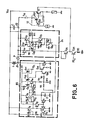
- the diagram in FIG. 5 is also similar to that in FIG. 4. It will however be noted that the transistor T2, instead of being constituted by a single transistor, is replaced by two transistors Q26 and Q27 themselves mounted in Darlington with a resistor R13 on the emitter of the transistor Q 2 7 , this resistance being equivalent to the resistance RE2 represented in FIG. 3A.
- auxiliary voltage that is to say ultimately the base current in the transistor Tl
- provision may be made to add to the circuit previously described in relation with FIG. 5 means using a detection of the current in the transistor T1.
- the transistor T1 is modified.
- an additional P diffusion is produced at the same time as the basic diffusion and close to it.
- An additional PNP transistor is thus formed, the emitter of which corresponds to the base of the transistor Tl, the base corresponds to the collector of the transistor Tl and the emitter is the additional P diffusion.
- the transistor T1 approaches a saturation regime, the potential of its base becomes greater than that of its collector.
- the base-emitter junction of the additional PNP transistor is polarized in the forward direction; there is then transmission of carriers, part of which can be collected by additional P broadcasting.
- This additional transistor therefore makes it possible to provide a signal indicative of the fact that the transistor T1 enters saturation.
- This indicative signal will be used in conjunction with the comparator Q20-Q21 previously described to better adjust the auxiliary voltage V.AUX.
- a diode Q29 is added between the connection of the resistor R8 at the base of the transistor Q20 and the collector of the transistor Q25.
- the connection point between this diode Q29 and the collector of transistor Q25 is connected to the collector of the auxiliary PNP transistor.
- the current collected by the collector of the auxiliary transistor will flow in the current source consti killed by transistor Q25.
- the current, previously called 125 passing through the resistor R8 will be reduced since the total current in the transistor Q25 remains constant.
- the diode Q29 is intended to prevent the collector of the additional transistor superimposed on the transistor T1 from being temporarily able to reach a higher potential than the supply voltage VCC, which would induce reverse conduction of this transistor.
Landscapes
- Engineering & Computer Science (AREA)
- Power Engineering (AREA)
- Amplifiers (AREA)
- Dc-Dc Converters (AREA)
- Electronic Switches (AREA)
- Bipolar Integrated Circuits (AREA)
Applications Claiming Priority (2)
| Application Number | Priority Date | Filing Date | Title |
|---|---|---|---|
| FR8513759 | 1985-09-17 | ||
| FR8513759A FR2587562B1 (fr) | 1985-09-17 | 1985-09-17 | Dispositif de commande d'un circuit de sortie d'un circuit integre |
Publications (2)
| Publication Number | Publication Date |
|---|---|
| EP0216697A1 true EP0216697A1 (de) | 1987-04-01 |
| EP0216697B1 EP0216697B1 (de) | 1990-01-03 |
Family
ID=9322977
Family Applications (1)
| Application Number | Title | Priority Date | Filing Date |
|---|---|---|---|
| EP86402009A Expired - Lifetime EP0216697B1 (de) | 1985-09-17 | 1986-09-12 | Steuervorrichtung für einen Ausgangskreis einer integrierten Schaltung |
Country Status (5)
| Country | Link |
|---|---|
| US (1) | US4734595A (de) |
| EP (1) | EP0216697B1 (de) |
| JP (1) | JPS6266709A (de) |
| DE (1) | DE3668105D1 (de) |
| FR (1) | FR2587562B1 (de) |
Cited By (1)
| Publication number | Priority date | Publication date | Assignee | Title |
|---|---|---|---|---|
| ES2286924A1 (es) * | 2003-07-29 | 2007-12-01 | Jose Gregorio Hernandez Sanchez | Nueva polarizacion para transistores bipolares. |
Families Citing this family (3)
| Publication number | Priority date | Publication date | Assignee | Title |
|---|---|---|---|---|
| JPH0728214B2 (ja) * | 1987-02-06 | 1995-03-29 | 株式会社日立製作所 | 半導体集積回路装置 |
| US5338980A (en) * | 1989-10-04 | 1994-08-16 | Texas Instruments Incorporated | Circuit for providing a high-speed logic transition |
| JP3598530B2 (ja) * | 1994-04-21 | 2004-12-08 | 株式会社日立製作所 | 活栓挿抜装置 |
Citations (2)
| Publication number | Priority date | Publication date | Assignee | Title |
|---|---|---|---|---|
| US4013940A (en) * | 1974-12-21 | 1977-03-22 | Naoyuki Maeda | Semiconductor circuit device |
| US4318164A (en) * | 1979-03-15 | 1982-03-02 | Tokyo Shibaura Denki Kabushiki Kaisha | High frequency switching circuit having preselected parameters to reduce power dissipation therein |
Family Cites Families (5)
| Publication number | Priority date | Publication date | Assignee | Title |
|---|---|---|---|---|
| JPS51122360A (en) * | 1975-04-18 | 1976-10-26 | Sony Corp | Improvement of darlington circuit |
| JPS52142231A (en) * | 1976-05-21 | 1977-11-28 | Isamu Kaji | Semiconductor circuits device |
| JPS5829206A (ja) * | 1982-07-29 | 1983-02-21 | Pioneer Electronic Corp | トランジスタ増巾器 |
| DE3333653C1 (de) * | 1983-09-17 | 1985-03-14 | Danfoss A/S, Nordborg | Elektronische Schaltvorrichtung |
| NL8400635A (nl) * | 1984-02-29 | 1985-09-16 | Philips Nv | Darlington transistorschakeling. |
-
1985
- 1985-09-17 FR FR8513759A patent/FR2587562B1/fr not_active Expired
-
1986
- 1986-09-12 DE DE8686402009T patent/DE3668105D1/de not_active Expired - Fee Related
- 1986-09-12 EP EP86402009A patent/EP0216697B1/de not_active Expired - Lifetime
- 1986-09-17 JP JP61219082A patent/JPS6266709A/ja active Pending
- 1986-09-17 US US06/908,673 patent/US4734595A/en not_active Expired - Lifetime
Patent Citations (2)
| Publication number | Priority date | Publication date | Assignee | Title |
|---|---|---|---|---|
| US4013940A (en) * | 1974-12-21 | 1977-03-22 | Naoyuki Maeda | Semiconductor circuit device |
| US4318164A (en) * | 1979-03-15 | 1982-03-02 | Tokyo Shibaura Denki Kabushiki Kaisha | High frequency switching circuit having preselected parameters to reduce power dissipation therein |
Non-Patent Citations (1)
| Title |
|---|
| PATENTS ABSTRACTS OF JAPAN, vol. 1, no. 30, page 1065 e 76, 29 mars 1977; & JP-A-51 122 360 (SONY K.K.) 26-10-1976 * |
Cited By (2)
| Publication number | Priority date | Publication date | Assignee | Title |
|---|---|---|---|---|
| ES2286924A1 (es) * | 2003-07-29 | 2007-12-01 | Jose Gregorio Hernandez Sanchez | Nueva polarizacion para transistores bipolares. |
| ES2286924B1 (es) * | 2003-07-29 | 2008-10-16 | Jose Gregorio Hernandez Sanchez | Nueva polarizacion para transistores bipolares. |
Also Published As
| Publication number | Publication date |
|---|---|
| FR2587562A1 (fr) | 1987-03-20 |
| EP0216697B1 (de) | 1990-01-03 |
| US4734595A (en) | 1988-03-29 |
| FR2587562B1 (fr) | 1987-11-20 |
| DE3668105D1 (de) | 1990-02-08 |
| JPS6266709A (ja) | 1987-03-26 |
Similar Documents
| Publication | Publication Date | Title |
|---|---|---|
| FR2819064A1 (fr) | Regulateur de tension a stabilite amelioree | |
| EP0903839A1 (de) | Spannungsregler | |
| EP0110775A1 (de) | Regulierungseinrichtung mit kleiner Verlustspannung | |
| EP0614282B1 (de) | Rauscharme Ladepumpe mit niedrigem Verbrauch und Frequenzsynthesizer, ausgestattet mit einer solchen Schaltung | |
| FR2548403A1 (fr) | Stabilisateur de tension integre monolithique a domaine d'utilisation etendu, pour des applications de type automobile | |
| FR2819652A1 (fr) | Regulateur de tension a rendement ameliore | |
| EP0815635B1 (de) | Leistungsversorgungsschaltung mit einem speicherkondensator | |
| FR2734429A1 (fr) | Module interrupteur et d'alimentation-application au demarrage d'un tube fluorescent | |
| FR2848356A1 (fr) | Procede de commande d'une alimentation a decoupage a un seul element inductif et plusieurs sorties, et alimentation correspondante, en particulier pour un telephone mobile cellulaire | |
| EP0194177B1 (de) | Teilnehmerschnittstellenschaltung mit Überwachungsbetrieb bei verringerter Speisung | |
| EP0216697B1 (de) | Steuervorrichtung für einen Ausgangskreis einer integrierten Schaltung | |
| EP0561456B1 (de) | Schneller Schaltstromspiegel | |
| FR2550028A1 (fr) | Circuit d'alimentation delivrant des tensions continues d'egale grandeur mais de polarite opposee, notamment pour appareils de reproduction sonore a bord d'automobiles | |
| EP0307325B1 (de) | Steuerungskreis für eine Zündung | |
| FR2732848A1 (fr) | Amplificateur de lecture de registre ccd | |
| FR2527399A1 (fr) | Circuit a impedance d'entree, elevee | |
| FR2460576A1 (fr) | Circuit d'alimentation a trois bornes pour appareil telephonique | |
| EP0782257A1 (de) | Widerstandsanpassung für eine Spannungsversorgungsleitung | |
| FR2728117A1 (fr) | Circuit de commande pour interrupteur electronique et interrupteur en faisant application | |
| EP0821469B1 (de) | Hoch- und Niederspannungsgleichstromversorgung | |
| EP0913754B1 (de) | Umschaltbare Gleichspannungsregelungsschaltung | |
| CH682019A5 (en) | Amplitude control circuit for oscillator circuit - includes current sources and current mirror in circuit to limit final output voltage of oscillator control circuit | |
| EP0881623B1 (de) | Schaltung zur Steuerung einer vibrierenden Membran | |
| EP0045691A2 (de) | Stufe mit niedriger Ausgangsimpedanz für kapazitive oder direkte Ankopplung | |
| EP0122820B1 (de) | Regler für einen Batterieladegenerator |
Legal Events
| Date | Code | Title | Description |
|---|---|---|---|
| PUAI | Public reference made under article 153(3) epc to a published international application that has entered the european phase |
Free format text: ORIGINAL CODE: 0009012 |
|
| AK | Designated contracting states |
Kind code of ref document: A1 Designated state(s): DE FR IT NL SE |
|
| 17P | Request for examination filed |
Effective date: 19870421 |
|
| 17Q | First examination report despatched |
Effective date: 19890412 |
|
| RAP3 | Party data changed (applicant data changed or rights of an application transferred) |
Owner name: THOMSON-CSF |
|
| GRAA | (expected) grant |
Free format text: ORIGINAL CODE: 0009210 |
|
| AK | Designated contracting states |
Kind code of ref document: B1 Designated state(s): DE FR IT NL SE |
|
| REF | Corresponds to: |
Ref document number: 3668105 Country of ref document: DE Date of ref document: 19900208 |
|
| ITF | It: translation for a ep patent filed | ||
| PGFP | Annual fee paid to national office [announced via postgrant information from national office to epo] |
Ref country code: NL Payment date: 19900930 Year of fee payment: 5 |
|
| PLBE | No opposition filed within time limit |
Free format text: ORIGINAL CODE: 0009261 |
|
| STAA | Information on the status of an ep patent application or granted ep patent |
Free format text: STATUS: NO OPPOSITION FILED WITHIN TIME LIMIT |
|
| 26N | No opposition filed | ||
| PGFP | Annual fee paid to national office [announced via postgrant information from national office to epo] |
Ref country code: SE Payment date: 19910820 Year of fee payment: 6 |
|
| ITTA | It: last paid annual fee | ||
| PG25 | Lapsed in a contracting state [announced via postgrant information from national office to epo] |
Ref country code: NL Effective date: 19920401 |
|
| NLV4 | Nl: lapsed or anulled due to non-payment of the annual fee | ||
| PG25 | Lapsed in a contracting state [announced via postgrant information from national office to epo] |
Ref country code: SE Effective date: 19920913 |
|
| EUG | Se: european patent has lapsed |
Ref document number: 86402009.4 Effective date: 19930406 |
|
| REG | Reference to a national code |
Ref country code: FR Ref legal event code: D6 |
|
| PGFP | Annual fee paid to national office [announced via postgrant information from national office to epo] |
Ref country code: DE Payment date: 20000904 Year of fee payment: 15 |
|
| PGFP | Annual fee paid to national office [announced via postgrant information from national office to epo] |
Ref country code: FR Payment date: 20000912 Year of fee payment: 15 |
|
| PG25 | Lapsed in a contracting state [announced via postgrant information from national office to epo] |
Ref country code: DE Free format text: LAPSE BECAUSE OF NON-PAYMENT OF DUE FEES Effective date: 20020501 |
|
| PG25 | Lapsed in a contracting state [announced via postgrant information from national office to epo] |
Ref country code: FR Free format text: LAPSE BECAUSE OF NON-PAYMENT OF DUE FEES Effective date: 20020531 |
|
| REG | Reference to a national code |
Ref country code: FR Ref legal event code: ST |
|
| PG25 | Lapsed in a contracting state [announced via postgrant information from national office to epo] |
Ref country code: IT Free format text: LAPSE BECAUSE OF NON-PAYMENT OF DUE FEES;WARNING: LAPSES OF ITALIAN PATENTS WITH EFFECTIVE DATE BEFORE 2007 MAY HAVE OCCURRED AT ANY TIME BEFORE 2007. THE CORRECT EFFECTIVE DATE MAY BE DIFFERENT FROM THE ONE RECORDED. Effective date: 20050912 |