EP0217224A2 - Convertisseur numérique-analogique à segments - Google Patents
Convertisseur numérique-analogique à segments Download PDFInfo
- Publication number
- EP0217224A2 EP0217224A2 EP86112802A EP86112802A EP0217224A2 EP 0217224 A2 EP0217224 A2 EP 0217224A2 EP 86112802 A EP86112802 A EP 86112802A EP 86112802 A EP86112802 A EP 86112802A EP 0217224 A2 EP0217224 A2 EP 0217224A2
- Authority
- EP
- European Patent Office
- Prior art keywords
- network
- resistors
- arrangement according
- segment
- digital
- Prior art date
- Legal status (The legal status is an assumption and is not a legal conclusion. Google has not performed a legal analysis and makes no representation as to the accuracy of the status listed.)
- Withdrawn
Links
Images
Classifications
-
- H—ELECTRICITY
- H03—ELECTRONIC CIRCUITRY
- H03M—CODING; DECODING; CODE CONVERSION IN GENERAL
- H03M1/00—Analogue/digital conversion; Digital/analogue conversion
- H03M1/06—Continuously compensating for, or preventing, undesired influence of physical parameters
-
- H—ELECTRICITY
- H03—ELECTRONIC CIRCUITRY
- H03M—CODING; DECODING; CODE CONVERSION IN GENERAL
- H03M1/00—Analogue/digital conversion; Digital/analogue conversion
- H03M1/66—Digital/analogue converters
- H03M1/74—Simultaneous conversion
- H03M1/78—Simultaneous conversion using ladder network
- H03M1/785—Simultaneous conversion using ladder network using resistors, i.e. R-2R ladders
Definitions
- the invention relates to a digital-to-analog converter according to the preamble of patent claim 1.
- Digital-to-analog converters based on the principle of the summation of weighted currents, in which weighted currents are generated and added using a reference voltage source and switchable weighted resistors, place the highest demands on the accuracy of the resistors at just a few weighting levels.
- the digital code to be evaluated which controls the switches and switches the weighted resistors to the summing node, requires, for example in the case of a dual code with ten bits, resistors with a relative accuracy better than ⁇ 0.05%.
- a digital-to-analog converter for 12 bits is no longer monotonous if the current of the most significant bit (MSB) falls below its setpoint by a fraction of 1/2048. This results in a relative accuracy of the resistances of ⁇ 0.0244%.
- a digital or analog adjustment of the resistors with the aid of lasers means a great deal of time and, depending on the resistors used, is only possible up to a certain number of bits. Correcting the output current of the digital-to-analog converter with the aid of a correction network means a great deal of effort.
- the invention is based on the object of specifying a digital-to-analog converter which, with a resolution of more than 9 bits long dual numbers, in particular with dual numbers with 12 bits, can do without a resistance comparison or a correction network for the R-2R network.
- the invention is based on the idea of jumping the main carry, ie jumping from a dual number, in which all bits except the MSB have the logical value 1 to a dual number, in which only the MSB has the logical value 1, in one number to split smaller jumps.
- an R-2R network is used, which without correction network or without matching the resistors.
- This network carries out a binary weighting of the least significant bits.
- the analog output current corresponding to the most significant bits is generated with the aid of a segment network which contains segments controlled by the most significant bits and which are connected in parallel with the R-2R network. According to the invention, this segment network is realized by resistors and switches.
- the digital-to-analog converter has the advantage of improved compensation for resistance inaccuracies, a simplified weighted resistor and switch network, a reduction in the current load on the resistors and a reduction in the influence of the substrate control factor if MOS transistors are used as resistors, which are connected appropriately .
- Embodiments of the inventive concept are characterized in the subclaims.
- the digital-to-analog converter contains a reference direct voltage source or a reference direct current source, which is connected to the input of a resistor and switch network according to the invention for converting the digital input codes is connected to an analog output current and an inverting operational amplifier, which is fed back via a resistor, for converting the output current of the resistor and switch network into an output voltage.
- the reference direct current source at the input of the digital-to-analog converter can be designed in accordance with the corresponding patent applications VPA 85 E 5303 and VPA 85 E 5306.
- the direct current source contains a current mirror formed from the n-channel metal oxide transistors MN1 and MN2.
- the current Io flowing through the input transistor MN1 results from an input reference voltage UREF present at the terminal VREF with respect to a reference potential GND with the aid of a resistor RS which determines the input current Io.
- the input current Io is kept constant with the help of an operational amplifier OPS.
- the input terminal VREF is connected to the inverting input of the operational amplifier OPS and the potential of the connection point of the output circuit of the transistor MN1 to the resistor RS is connected to the non-inverting input of the operational amplifier.
- the other connection of the resistor RS is connected to the reference potential GND.
- the gate of the input transistor MN1 and the gate of the output transistor MN2 of the current mirror are connected to one another and to the output of the operational amplifier OPS.
- the connections of the output circuits of the transistors MN1 and MN2 which serve as the source are jointly connected to a terminal VSS.
- the output of the current source is formed by the terminal SA, which is connected to the connection of the output transistor MN2 serving as a drain the current mirror is connected.
- the reference current IREF resulting according to the transformation ratio of the two transistors of the current mirror flows as a function of the input current Io of the current mirror.
- the terminal SA has the input voltage UE compared to the reference potential GND.
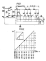
- the resistor network according to the invention contains, starting from the input terminal SA as an input node, parallel resistors 2R, to which a known R-2R network is connected in parallel via a resistor R. With the exception of the load resistor 2R of the R-2R network, the output-side connections of the resistors 2R of this network and the output-side connections of the parallel resistors are each connected to the connections of assigned switches which carry current in both switching positions. Another connection of the switches and the output connection of the load resistor 2R are connected to the reference potential GND.
- the third connection of the two-way switches is connected to the inverting input of an operational amplifier OPA which is coupled back via a resistor RG, the output of which is connected to the terminal VA, which represents the output terminal of the digital-to-analog converter and has the voltage UA with respect to the reference voltage GND.
- the switches assigned to the R-2R network are provided with the reference symbols S o to S n-1 and S n in accordance with the binary weighting of the binary digital partial code which controls the switches.
- the switches of the segments of the segment network connected in parallel with this network are identified by the reference symbols S 1 to S n-1 and S n .
- the value of the individual resistors of the segment network connected in parallel is the same size and the same size as the input resistance of the R-2R network.
- Either the segment resistors have the value R or, as in FIG. 1, the value 2R, in which case the R-2R network is connected to the segment network via a further resistor R in series with the R-2R network.
- the reference current IREF which flows into the input SA of the network according to the invention, is divided into a number of equally large partial currents, the partial current flowing into the R-2R network being divided there in a binary weighted manner.
- the most significant bits (MSBs) of the digital input code are used to control the switches S 1 to S n of the segments of the segment network.
- the bits used for the control of the switches S 1 to S n of the segments must be decoded, since the individual segment currents are of the same size and are not binary-weighted, as in the R-2R network.
- the number of bits required to control the switches of the segments results from the number of segments.
- the function of a circuit according to the invention according to FIG. 1 can be explained on the basis of the diagram according to FIG. 2.
- the diagram shows the input / output characteristic for a 12-bit digital-to-analog converter.
- the 4096 possible stages of the digital-to-analog converter are realized with a segmentation of 8 ⁇ 512 stages.
- a 9-bit R-2R network is provided for the 512 digital stages, which carries out a binary weighting.
- a segment network with 7 segments is required for the 8 levels.
- the digital input word controlling the switches of the network according to the invention is "digital in” in binary code at intervals of 512 bits each applied.
- the ordinate is designated by the analog output current Iout, which flows into the inverting input of the operational amplifier OPA.
- linear characteristic of the analog output current as a function of the digital input code is divided in the ordinate direction into eight linear subsections with the respective summed segment currents I1 to I7 which result if none or all of the switches S 1 to S n on the inverting input of the Operational amplifier OPA are connected.
- the seven resistors of the segments, each with the value 2R, must be accurate to 12 bits.
- the R-2R network only needs to be accurate to 9 bits corresponding to 512 levels, i.e. the resistances of this network can have a relative accuracy of ⁇ 0.2% without the R-2R network having to be corrected.
- the main carry of the digital-to-analog converter i.e. the transfer from the dual number 011 111 111 to the dual number 100,000,000 is repeated in each of the segments and is therefore 4 times less critical than the main transfer in a pure R-2R network for 12 bits.
- the transmission characteristic of the digital-to-analog converter according to the invention has a smaller lineari with the same resistance tolerance the transmission characteristic of a pure R-2R network for 12 bits.
- the differential non-linearity ie the deviation of the distance between two adjacent analog values from the ideal 1-LSB distance, is also improved in a digital-to-analog converter according to the invention, so that monotony is achieved with a greater resistance tolerance than in a conventional 12-bit R-2R -Network.
- the uniform step size is more important than the best possible adaptation of the converter characteristic to an ideal straight line, since there are few transducers with a linearity better than 0.1%.
- the resistances of the R-2R network must be accurate to ⁇ 0.4%. In this case, he however, the number of segment resistances to be corrected or adjusted increases to 15.
- polysilicon resistors can also be used, which can be manufactured with an achievable relative accuracy of better than 1%. Without correction or Adjustment measures can be resolved with 7 bits. For a 12 bit converter, the five MSBs must therefore be corrected or adjusted. Adjustment measures are advantageously carried out by laser trimming, whereby a digital adjustment due to the severing of conductor tracks is less precise than an analog adjustment, but requires less time.
- MOS transistors wired as resistors are also advantageously suitable as resistors for the resistor network.
- the influence of the substrate control factor can be reduced, which influences the R on value via the threshold voltage.
- the segmentation reduces the different substrate voltages resulting from the series resistances R of the R-2R network, which have a direct effect on the threshold voltages and the R on value.
- Another way to achieve the required resolution is to correct the output current Iout using a correction network.
- the deviation of the output current from the setpoint is determined and saved.
- the error of the output current is corrected in the digital-to-analog conversion by the correction network, for example an error-correction digital-to-analog converter.
- the network error can be measured by an additional circuit directly on the chip and saved in a memory with random access (RAM).
- RAM random access
- the network error can be detected at any time and the RAM reprogrammed. This form of correction thus also records aging processes and, in part, the temperature response of the network carrying out the digital-analog conversion.
- the correction network can also be controlled by a programmable read-only memory (PROM), in which the error of the network under conditions to be determined, e.g. the temperature, determined only once and the PROM is programmed accordingly.
- PROM programmable read-only memory
- this form of correction also has the advantage that the PROM does not have to be programmed until the chip has been installed. Errors that result from sawing the window or mounting the chip are taken into account by the correction.
- the temperature response of a digital-to-analog converter according to the invention shown in FIG. 1 can be completely compensated in a first approximation if the reference voltage UREF at the terminal VREF of the converter is converted into a reference current IREF that feeds the network and the resistor RS of this is converted using a resistor RS Current source has the same temperature response as the resistor RG in the negative feedback branch of the inverting output operational amplifier OPA.
- a derar compensation of the temperature responses of digital-to-analog converters is specified in the corresponding patent application VPA 85 E 5306. It also provides that the reference current IREF can have different polarities and thus the output voltage UA of the digital-to-analog converter can be bipolar depending on the desired application.
Landscapes
- Engineering & Computer Science (AREA)
- Theoretical Computer Science (AREA)
- Analogue/Digital Conversion (AREA)
Applications Claiming Priority (2)
| Application Number | Priority Date | Filing Date | Title |
|---|---|---|---|
| DE3534862 | 1985-09-30 | ||
| DE3534862 | 1985-09-30 |
Publications (2)
| Publication Number | Publication Date |
|---|---|
| EP0217224A2 true EP0217224A2 (fr) | 1987-04-08 |
| EP0217224A3 EP0217224A3 (fr) | 1987-07-01 |
Family
ID=6282374
Family Applications (1)
| Application Number | Title | Priority Date | Filing Date |
|---|---|---|---|
| EP86112802A Withdrawn EP0217224A3 (fr) | 1985-09-30 | 1986-09-16 | Convertisseur numérique-analogique à segments |
Country Status (2)
| Country | Link |
|---|---|
| EP (1) | EP0217224A3 (fr) |
| JP (1) | JPS6282822A (fr) |
Cited By (3)
| Publication number | Priority date | Publication date | Assignee | Title |
|---|---|---|---|---|
| EP0325378A3 (fr) * | 1988-01-21 | 1992-02-26 | Advanced Micro Devices, Inc. | Convertisseur numérique-analogique |
| EP0638913A1 (fr) * | 1993-08-12 | 1995-02-15 | Societe Nationale D'etude Et De Construction De Moteurs D'aviation "Snecma" | Circuit de détection de la position de plusieurs contacteurs bipolaires et application à un inverseur de poussée d'un turboréacteur |
| EP1298800A1 (fr) * | 2001-09-28 | 2003-04-02 | STMicroelectronics Limited | Générateur de rampe |
Families Citing this family (1)
| Publication number | Priority date | Publication date | Assignee | Title |
|---|---|---|---|---|
| KR0176745B1 (ko) * | 1989-07-31 | 1999-05-15 | 이헌조 | 서보모터의 속도제어회로 |
Family Cites Families (2)
| Publication number | Priority date | Publication date | Assignee | Title |
|---|---|---|---|---|
| US4029949A (en) * | 1975-07-08 | 1977-06-14 | The Charles Stark Draper Laboratory, Inc. | Servo-controlled microscope stage |
| US4338592A (en) * | 1980-02-11 | 1982-07-06 | Hybrid Systems Corporation | High accuracy digital-to-analog converter and transient elimination system thereof |
-
1986
- 1986-09-16 EP EP86112802A patent/EP0217224A3/fr not_active Withdrawn
- 1986-09-29 JP JP61231082A patent/JPS6282822A/ja active Pending
Cited By (6)
| Publication number | Priority date | Publication date | Assignee | Title |
|---|---|---|---|---|
| EP0325378A3 (fr) * | 1988-01-21 | 1992-02-26 | Advanced Micro Devices, Inc. | Convertisseur numérique-analogique |
| EP0638913A1 (fr) * | 1993-08-12 | 1995-02-15 | Societe Nationale D'etude Et De Construction De Moteurs D'aviation "Snecma" | Circuit de détection de la position de plusieurs contacteurs bipolaires et application à un inverseur de poussée d'un turboréacteur |
| FR2709017A1 (fr) * | 1993-08-12 | 1995-02-17 | Snecma | Circuit de détection de la position de plusieurs contacteurs bipolaires et application à un inverseur de poussée d'un turboréacteur. |
| US5508626A (en) * | 1993-08-12 | 1996-04-16 | Societe Nationale D'etude Et De Construction De Moteurs D'aviation "Snecma" | Circuit for detecting the position of several bipolar contactors and application for a thrust reverser of a turbojet engine |
| EP1298800A1 (fr) * | 2001-09-28 | 2003-04-02 | STMicroelectronics Limited | Générateur de rampe |
| US6956413B2 (en) | 2001-09-28 | 2005-10-18 | Stmicroelectronics Ltd. | Ramp generator for image sensor ADC |
Also Published As
| Publication number | Publication date |
|---|---|
| JPS6282822A (ja) | 1987-04-16 |
| EP0217224A3 (fr) | 1987-07-01 |
Similar Documents
| Publication | Publication Date | Title |
|---|---|---|
| DE69434102T2 (de) | Digital-Analog-Wandler | |
| DE69836871T2 (de) | R/2r-leiterschaltung und verfahren für einen digital-analog-wandler | |
| DE112014001378B4 (de) | Mehrketten-Digital-Analog-Wandler | |
| DE69601143T2 (de) | Digital-Analogwandler und Verfahren zur Generierung einer in etwa stückweise linearen Wellenform | |
| DE60114051T2 (de) | Selbstangleichende stromquelle und verfahren für einen daw mit geschalteten stromquellen | |
| DE60205526T2 (de) | Digital-Analog-Wandler mit Stromquellenanordnung | |
| DE3311067A1 (de) | Digital-analog-wandler hohen aufloesevermoegens | |
| DE69327602T2 (de) | Analog-/Digitalumsetzer mit Kapazitätsnetzwerk | |
| DE68914682T2 (de) | Digital-analogwandler mit auf der platte eingebautem invertierungsverstärker mit einheitsverstärkung. | |
| WO1997043833A1 (fr) | Architecture de commutateurs amelioree pour convertisseurs de numerique en analogique r/2r | |
| DE3241364C2 (fr) | ||
| DE68926184T2 (de) | DA-Wandler | |
| DE68926171T2 (de) | Digital-Analogwandler | |
| DE2706931C2 (fr) | ||
| EP0217223B1 (fr) | Convertisseur numérique-analogique à compensation de température | |
| DE102008006079B4 (de) | Programmierbarer Stromerzeuger, Stromerzeugungsverfahren und Senderanordnung | |
| US9317054B2 (en) | Feedback network for low-drop-out generator | |
| US7348912B2 (en) | High resolution and low consumption digital-to-analog converter | |
| DE3306310C2 (fr) | ||
| DE3129797C2 (fr) | ||
| DE3145889A1 (de) | Integrierbarer digital/analog-wandler | |
| EP0442321A2 (fr) | Convertisseur analogique-numérique simultané étendu | |
| DE3876199T2 (de) | Einstellbare stromquelle und ein digital-analoger wandler mit automatischer eichung und verwendung einer solchen quelle. | |
| DE69520562T2 (de) | Quadratischer Digital-Analogumsetzer | |
| DE3516005A1 (de) | Digital-analog-wandler |
Legal Events
| Date | Code | Title | Description |
|---|---|---|---|
| PUAI | Public reference made under article 153(3) epc to a published international application that has entered the european phase |
Free format text: ORIGINAL CODE: 0009012 |
|
| AK | Designated contracting states |
Kind code of ref document: A2 Designated state(s): AT BE CH DE FR GB IT LI LU NL SE |
|
| PUAL | Search report despatched |
Free format text: ORIGINAL CODE: 0009013 |
|
| AK | Designated contracting states |
Kind code of ref document: A3 Designated state(s): AT BE CH DE FR GB IT LI LU NL SE |
|
| STAA | Information on the status of an ep patent application or granted ep patent |
Free format text: STATUS: THE APPLICATION IS DEEMED TO BE WITHDRAWN |
|
| 18D | Application deemed to be withdrawn |
Effective date: 19880105 |
|
| RIN1 | Information on inventor provided before grant (corrected) |
Inventor name: DIELACHER, FRANZ, DIPL.-ING. |