EP0217844B1 - Verfahren zur herstellung einer flüssigkristall-anzeigevorrichtung mit einer dioden-matrix - Google Patents
Verfahren zur herstellung einer flüssigkristall-anzeigevorrichtung mit einer dioden-matrix Download PDFInfo
- Publication number
- EP0217844B1 EP0217844B1 EP86901894A EP86901894A EP0217844B1 EP 0217844 B1 EP0217844 B1 EP 0217844B1 EP 86901894 A EP86901894 A EP 86901894A EP 86901894 A EP86901894 A EP 86901894A EP 0217844 B1 EP0217844 B1 EP 0217844B1
- Authority
- EP
- European Patent Office
- Prior art keywords
- conductive material
- asi
- bridge
- layer
- diodes
- Prior art date
- Legal status (The legal status is an assumption and is not a legal conclusion. Google has not performed a legal analysis and makes no representation as to the accuracy of the status listed.)
- Expired - Lifetime
Links
- 238000000034 method Methods 0.000 title claims abstract description 18
- 238000004519 manufacturing process Methods 0.000 title claims description 10
- 239000004973 liquid crystal related substance Substances 0.000 title claims description 6
- 239000004020 conductor Substances 0.000 claims description 33
- 229910021417 amorphous silicon Inorganic materials 0.000 claims description 18
- BASFCYQUMIYNBI-UHFFFAOYSA-N platinum Chemical compound [Pt] BASFCYQUMIYNBI-UHFFFAOYSA-N 0.000 claims description 13
- VYZAMTAEIAYCRO-UHFFFAOYSA-N Chromium Chemical compound [Cr] VYZAMTAEIAYCRO-UHFFFAOYSA-N 0.000 claims description 12
- 229910052804 chromium Inorganic materials 0.000 claims description 10
- 239000011651 chromium Substances 0.000 claims description 10
- 239000011159 matrix material Substances 0.000 claims description 9
- 229910052751 metal Inorganic materials 0.000 claims description 8
- 239000002184 metal Substances 0.000 claims description 8
- 229910052697 platinum Inorganic materials 0.000 claims description 7
- 239000000758 substrate Substances 0.000 claims description 4
- 239000000463 material Substances 0.000 claims description 2
- 238000000151 deposition Methods 0.000 claims 1
- 238000010276 construction Methods 0.000 abstract 1
- 239000010410 layer Substances 0.000 description 47
- XUIMIQQOPSSXEZ-UHFFFAOYSA-N Silicon Chemical compound [Si] XUIMIQQOPSSXEZ-UHFFFAOYSA-N 0.000 description 5
- 238000010586 diagram Methods 0.000 description 4
- 230000005284 excitation Effects 0.000 description 3
- 230000000873 masking effect Effects 0.000 description 3
- GUVRBAGPIYLISA-UHFFFAOYSA-N tantalum atom Chemical compound [Ta] GUVRBAGPIYLISA-UHFFFAOYSA-N 0.000 description 3
- 239000004642 Polyimide Substances 0.000 description 2
- 240000008042 Zea mays Species 0.000 description 2
- 229910052782 aluminium Inorganic materials 0.000 description 2
- XAGFODPZIPBFFR-UHFFFAOYSA-N aluminium Chemical compound [Al] XAGFODPZIPBFFR-UHFFFAOYSA-N 0.000 description 2
- 230000015572 biosynthetic process Effects 0.000 description 2
- 239000003990 capacitor Substances 0.000 description 2
- 230000000694 effects Effects 0.000 description 2
- 229910052738 indium Inorganic materials 0.000 description 2
- APFVFJFRJDLVQX-UHFFFAOYSA-N indium atom Chemical compound [In] APFVFJFRJDLVQX-UHFFFAOYSA-N 0.000 description 2
- 230000003287 optical effect Effects 0.000 description 2
- 238000000206 photolithography Methods 0.000 description 2
- 229920001721 polyimide Polymers 0.000 description 2
- 239000010409 thin film Substances 0.000 description 2
- 241001415961 Gaviidae Species 0.000 description 1
- ATJFFYVFTNAWJD-UHFFFAOYSA-N Tin Chemical compound [Sn] ATJFFYVFTNAWJD-UHFFFAOYSA-N 0.000 description 1
- 241001639412 Verres Species 0.000 description 1
- 239000004411 aluminium Substances 0.000 description 1
- 230000008021 deposition Effects 0.000 description 1
- 229940082150 encore Drugs 0.000 description 1
- 238000005530 etching Methods 0.000 description 1
- 239000011521 glass Substances 0.000 description 1
- 229910003437 indium oxide Inorganic materials 0.000 description 1
- PJXISJQVUVHSOJ-UHFFFAOYSA-N indium(iii) oxide Chemical compound [O-2].[O-2].[O-2].[In+3].[In+3] PJXISJQVUVHSOJ-UHFFFAOYSA-N 0.000 description 1
- AMGQUBHHOARCQH-UHFFFAOYSA-N indium;oxotin Chemical compound [In].[Sn]=O AMGQUBHHOARCQH-UHFFFAOYSA-N 0.000 description 1
- 238000009413 insulation Methods 0.000 description 1
- 239000011229 interlayer Substances 0.000 description 1
- 230000004048 modification Effects 0.000 description 1
- 238000012986 modification Methods 0.000 description 1
- BPUBBGLMJRNUCC-UHFFFAOYSA-N oxygen(2-);tantalum(5+) Chemical compound [O-2].[O-2].[O-2].[O-2].[O-2].[Ta+5].[Ta+5] BPUBBGLMJRNUCC-UHFFFAOYSA-N 0.000 description 1
- 229910052710 silicon Inorganic materials 0.000 description 1
- 239000010703 silicon Substances 0.000 description 1
- 229910052715 tantalum Inorganic materials 0.000 description 1
- PBCFLUZVCVVTBY-UHFFFAOYSA-N tantalum pentoxide Inorganic materials O=[Ta](=O)O[Ta](=O)=O PBCFLUZVCVVTBY-UHFFFAOYSA-N 0.000 description 1
- 229910001887 tin oxide Inorganic materials 0.000 description 1
Images
Classifications
-
- G—PHYSICS
- G02—OPTICS
- G02F—OPTICAL DEVICES OR ARRANGEMENTS FOR THE CONTROL OF LIGHT BY MODIFICATION OF THE OPTICAL PROPERTIES OF THE MEDIA OF THE ELEMENTS INVOLVED THEREIN; NON-LINEAR OPTICS; FREQUENCY-CHANGING OF LIGHT; OPTICAL LOGIC ELEMENTS; OPTICAL ANALOGUE/DIGITAL CONVERTERS
- G02F1/00—Devices or arrangements for the control of the intensity, colour, phase, polarisation or direction of light arriving from an independent light source, e.g. switching, gating or modulating; Non-linear optics
- G02F1/01—Devices or arrangements for the control of the intensity, colour, phase, polarisation or direction of light arriving from an independent light source, e.g. switching, gating or modulating; Non-linear optics for the control of the intensity, phase, polarisation or colour
- G02F1/13—Devices or arrangements for the control of the intensity, colour, phase, polarisation or direction of light arriving from an independent light source, e.g. switching, gating or modulating; Non-linear optics for the control of the intensity, phase, polarisation or colour based on liquid crystals, e.g. single liquid crystal display cells
- G02F1/133—Constructional arrangements; Operation of liquid crystal cells; Circuit arrangements
- G02F1/136—Liquid crystal cells structurally associated with a semi-conducting layer or substrate, e.g. cells forming part of an integrated circuit
- G02F1/1362—Active matrix addressed cells
- G02F1/1365—Active matrix addressed cells in which the switching element is a two-electrode device
Definitions
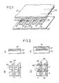
- the present invention relates to a method of manufacturing a liquid crystal display screen and diode network.
- Figure 1 attached shows a display screen of a known type which consists of an upper plate 10 covered with transparent conductive strips 12 oriented along parallel lines and a lower plate 20 covered with a matrix of blocks 22 and transparent conductive strips 24 oriented in parallel columns. These two plates are assembled and kept apart by a shim and a liquid crystal is introduced into the space between them. Each block constitutes an elementary display area (or "point"). A block is electrically connected to the adjacent column by a bridge 26. The excitation of a point Pij of the matrix is obtained by application of appropriate voltages on the line Li of the upper plate and on the column Cj of the lower plate .
- bridges 26 are known. Some use transistors (and in particular thin film transistors); others use non-linear elements such as diodes, which increases the number of addressable rows and columns, and therefore the number of display points.
- the present invention relates to a method of manufacturing such a screen, and more specifically relates to the production of bridges 26 in the variant using diodes.
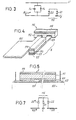
- the object of the present invention is precisely a method which avoids these drawbacks. Thanks to the invention, it is possible, in only two photolithography operations, to form a diode bridge between each block and the adjacent column. The bridge obtained is formed by two diodes mounted head to tail.
- the method of the invention uses pavers which have a rectangular shape with an appendage (or two) which are reminiscent of those described in document FR-A-2533072.
- the conductive bridge connecting each block to the adjacent column is a thin film transistor (TCM), which obviously involves different operations and layers.
- the first conductive material is made of amorphous silicon n + doped and the second conductive material is a metal, the latter forming Schottky contact with the aSi: H (i) which it covers; the two diodes formed in each bridge are then Schottky diodes.
- the first conductive material which is a metal forming with the aSi: H (i) which covers it a Schottky contact and the second conductive material is amorphous hydrogenated doped n + silicon; the two diodes formed in each bridge are still of the Schottky type.
- the first conductive material is p + (or n + ) doped aSi: H and the second conductive material n + (or p + ) doped aSi: H; the two diodes formed in each bridge are then of the p + in + type.
- the upper plate of the screen as illustrated in FIG. 1 (reference 10), is passed over in silence, since it is obtained by conventional means (deposition of an ITO layer then etching) .
- Layers 103-110-114 are chosen such that a diode-like structure is formed.
- second conductive material 114 of platinum or chromium, which form with the aSi: H of layer 110 a Schottky contact.
- other combinations are possible, as will be seen more clearly in FIGS. 8a, b and c.
- a first diode is obtained opposite each appendage 108 and a second diode is opposite each column, these two diodes being arranged in a similar manner.
- the equivalent electrical diagram of a display point Pij is represented in FIG. 3. This point is equivalent to a capacitor, the armatures of which are formed by the block of the lower plate and the part of the line situated opposite this block. on the upper plate, this capacitor having a capacity XL, with a resistance in parallel of value RL.
- This RC dipole is connected, on the one hand, to line Li and, on the other hand, through point 116, to column Cj, this bridge comprising two diodes D1, D2 mounted head to tail.
- FIG. 4 represents in perspective the layers obtained at the level of a bridge 116 and of a segment S. We see there the stack 103-110-114 forming the bridge of head-to-tail diodes between a column and the neighboring block and a segment S partially covering a column.
- FIG. 5 makes it possible to better understand how the stack which remains on the columns can play, in the event of the column being cut, the role of conductive bridge between the two parts of the column.
- the conductive bridge formed by the segment S and in particular by the conductive layer 103 restores electrical continuity.
- the stack S produces an optical masking of the column. If this column is not hidden, it is visible just like a display point. Its appearance depends on the average value of the video voltage during an image. This effect is very annoying in the white display mode on a black background, because the eye is very sensitive to white lines, even very fine. In the other mode, black on a white background, the effect is much less visible, a black line 20 ⁇ m wide on a white background being invisible to the eye. Optical masking of the transparent columns is therefore necessary especially in the first mode and it is perfectly obtained by the invention.
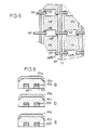
- each block 106 is associated with an appendix 108, by means of which the electrical connection is made with the preceding column.
- each block comprises a second appendage 108 * , diagonally opposite the first and allowing an electrical connection with the column which follows.
- Each block is then connected by two bridges of head-to-tail diodes to the addressing columns.
- Each block 106 includes a first appendix 108 in the upper left corner and a second appendix 108 * in the lower right corner.
- Each bridge 116 connects a column of row j to the appendix 108 of the block corresponding to the line i and located to the right of the column j and to the appendix 108 * of the block corresponding to the line i-1 located to the left of the column j.
- FIG. 7 shows the equivalent electrical diagram of such a bridge: the diode D1 at the level of column C and the diodes D2, D2 * at the level of the appendices 108 and 108 *.
- the presence of the second diode bridge Dl-D2 * slightly modifies the addressing process of each point, in the sense that the excited point Pij, instead of memorizing the excitation corresponding to the line Li and to the column Cj , will memorize the last excitation received, in this case the second (if there is no break), which corresponds to the line Li + 1 and to the column Cj + 1. But this modification is, in most cases, unimportant, since it simply amounts to shifting the displayed image by a row interval and a column interval.
- the layer 102 remains in ITO in the three cases.
Landscapes
- Physics & Mathematics (AREA)
- Nonlinear Science (AREA)
- Engineering & Computer Science (AREA)
- Microelectronics & Electronic Packaging (AREA)
- Mathematical Physics (AREA)
- Chemical & Material Sciences (AREA)
- Crystallography & Structural Chemistry (AREA)
- General Physics & Mathematics (AREA)
- Optics & Photonics (AREA)
- Liquid Crystal (AREA)
Claims (7)
Applications Claiming Priority (2)
| Application Number | Priority Date | Filing Date | Title |
|---|---|---|---|
| FR8504480 | 1985-03-26 | ||
| FR8504480A FR2579806B1 (fr) | 1985-03-26 | 1985-03-26 | Procede de fabrication d'un ecran d'affichage a cristaux liquides et a reseau de diodes |
Publications (2)
| Publication Number | Publication Date |
|---|---|
| EP0217844A1 EP0217844A1 (de) | 1987-04-15 |
| EP0217844B1 true EP0217844B1 (de) | 1990-05-23 |
Family
ID=9317588
Family Applications (1)
| Application Number | Title | Priority Date | Filing Date |
|---|---|---|---|
| EP86901894A Expired - Lifetime EP0217844B1 (de) | 1985-03-26 | 1986-03-13 | Verfahren zur herstellung einer flüssigkristall-anzeigevorrichtung mit einer dioden-matrix |
Country Status (7)
| Country | Link |
|---|---|
| US (1) | US4836650A (de) |
| EP (1) | EP0217844B1 (de) |
| JP (1) | JP2632153B2 (de) |
| CA (1) | CA1261952A (de) |
| DE (1) | DE3671544D1 (de) |
| FR (1) | FR2579806B1 (de) |
| WO (1) | WO1986005893A1 (de) |
Families Citing this family (10)
| Publication number | Priority date | Publication date | Assignee | Title |
|---|---|---|---|---|
| JPH02137366A (ja) * | 1988-11-18 | 1990-05-25 | Nec Corp | ダイオード型アクティブマトリクス基板 |
| NL8802997A (nl) * | 1988-12-07 | 1990-07-02 | Philips Nv | Weergeefinrichting. |
| FR2651371B1 (fr) * | 1989-08-29 | 1991-10-18 | France Etat | Procede de realisation d'un ecran d'affichage a matrice active et a structure inversee. |
| FR2662290B1 (fr) * | 1990-05-15 | 1992-07-24 | France Telecom | Procede de realisation d'un ecran d'affichage a matrice active et a condensateurs de stockage et ecran obtenu par ce procede. |
| GB9122173D0 (en) * | 1991-10-18 | 1991-11-27 | Philips Electronic Associated | Liquid crystal colour display device |
| JP3092761B2 (ja) * | 1991-12-02 | 2000-09-25 | キヤノン株式会社 | 画像表示装置及びその製造方法 |
| NL194873C (nl) * | 1992-08-13 | 2003-05-06 | Oki Electric Ind Co Ltd | Dunnefilmtransistorenreeks en daarvan gebruikmakende vloeibare kristalweergeefinrichting. |
| DE19530525A1 (de) * | 1995-08-19 | 1997-02-20 | Daimler Benz Ag | Schaltkreis mit monolithisch integrierter PIN-/Schottky-Diodenanordnung |
| US20080205010A1 (en) * | 2007-02-26 | 2008-08-28 | 3M Innovative Properties Company | Active matrix backplanes allowing relaxed alignment tolerance |
| US7629206B2 (en) * | 2007-02-26 | 2009-12-08 | 3M Innovative Properties Company | Patterning self-aligned transistors using back surface illumination |
Family Cites Families (17)
| Publication number | Priority date | Publication date | Assignee | Title |
|---|---|---|---|---|
| US4112333A (en) * | 1977-03-23 | 1978-09-05 | Westinghouse Electric Corp. | Display panel with integral memory capability for each display element and addressing system |
| US4237150A (en) * | 1979-04-18 | 1980-12-02 | The United States Of America As Represented By The United States Department Of Energy | Method of producing hydrogenated amorphous silicon film |
| DE3113041A1 (de) * | 1980-04-01 | 1982-01-28 | Canon K.K., Tokyo | Verfahren und vorrichtung zur anzeige von informationen |
| FR2505070B1 (fr) * | 1981-01-16 | 1986-04-04 | Suwa Seikosha Kk | Dispositif non lineaire pour un panneau d'affichage a cristaux liquides et procede de fabrication d'un tel panneau d'affichage |
| FR2518788A1 (fr) * | 1981-12-23 | 1983-06-24 | Thomson Csf | Dispositif a resistance dependant de la tension, son procede de fabrication et sa mise en oeuvre dans un ecran de visualisation a commande electrique |
| JPS58126518A (ja) * | 1982-01-25 | 1983-07-28 | Seiko Epson Corp | 液晶表示装置 |
| JPS6010706A (ja) * | 1983-06-30 | 1985-01-19 | Matsushita Electric Works Ltd | 3安定型電磁石装置 |
| FR2533072B1 (fr) * | 1982-09-14 | 1986-07-18 | Coissard Pierre | Procede de fabrication de circuits electroniques a base de transistors en couches minces et de condensateurs |
| US4545111A (en) * | 1983-01-18 | 1985-10-08 | Energy Conversion Devices, Inc. | Method for making, parallel preprogramming or field programming of electronic matrix arrays |
| JPS6010707A (ja) * | 1983-06-30 | 1985-01-19 | Matsushita Electric Works Ltd | 3安定型電磁石装置 |
| FR2551244B1 (fr) * | 1983-08-26 | 1985-10-11 | Thomson Csf | Procede de fabrication d'un substrat pour dispositif a commande electrique et ecran de visualisation elabore a partir d'un tel substrat |
| FR2551902B1 (fr) * | 1983-09-13 | 1986-01-24 | Thomson Csf | Ecran de visualisation a adressage par elements non lineaires et son procede de fabrication |
| EP0150728A3 (de) * | 1984-01-23 | 1986-01-08 | Energy Conversion Devices, Inc. | Mit Dioden aus amorphen Silizium-Legierungen gesteuerte Flüssigkristallanzeigevorrichtungen |
| FR2566583B1 (fr) * | 1984-06-22 | 1986-09-19 | Thomson Csf | Procede de fabrication d'au moins un transistor a effet de champ en couche mince, et transistor obtenu par ce procede |
| US4666252A (en) * | 1984-06-29 | 1987-05-19 | Energy Conversion Devices, Inc. | High yield liquid crystal display and method of making same |
| US4728172A (en) * | 1984-08-08 | 1988-03-01 | Energy Conversion Devices, Inc. | Subassemblies for displays having pixels with two portions and capacitors |
| US4715685A (en) * | 1985-03-04 | 1987-12-29 | Energy Conversion Devices, Inc. | Liquid crystal display having potential source in a diode ring |
-
1985
- 1985-03-26 FR FR8504480A patent/FR2579806B1/fr not_active Expired
-
1986
- 1986-03-13 JP JP61502149A patent/JP2632153B2/ja not_active Expired - Fee Related
- 1986-03-13 US US06/934,613 patent/US4836650A/en not_active Expired - Lifetime
- 1986-03-13 EP EP86901894A patent/EP0217844B1/de not_active Expired - Lifetime
- 1986-03-13 WO PCT/FR1986/000084 patent/WO1986005893A1/fr not_active Ceased
- 1986-03-13 DE DE8686901894T patent/DE3671544D1/de not_active Expired - Lifetime
- 1986-03-24 CA CA000504881A patent/CA1261952A/fr not_active Expired
Also Published As
| Publication number | Publication date |
|---|---|
| FR2579806B1 (fr) | 1987-05-07 |
| US4836650A (en) | 1989-06-06 |
| DE3671544D1 (de) | 1990-06-28 |
| EP0217844A1 (de) | 1987-04-15 |
| WO1986005893A1 (fr) | 1986-10-09 |
| CA1261952A (fr) | 1989-09-26 |
| JP2632153B2 (ja) | 1997-07-23 |
| FR2579806A1 (fr) | 1986-10-03 |
| JPS62502361A (ja) | 1987-09-10 |
Similar Documents
| Publication | Publication Date | Title |
|---|---|---|
| EP0524067B1 (de) | Hochauflösender Flüssigkristallbildschirm mit aktiver Matrix | |
| EP0267824B1 (de) | Transistor-gesteuerter elektrooptischer Anzeigeschirm und Verfahren zu seiner Herstellung | |
| FR2623649A1 (fr) | Cellule d'affichage a cristal liquide | |
| FR2585167A1 (fr) | Structures conductrices redondantes pour affichages a cristaux liquides commandes par des transistors a effet de champ en couche mince | |
| FR2593630A1 (fr) | Ecran d'affichage a matrice active a resistance de drain et procedes de fabrication de cet ecran | |
| FR2700062A1 (fr) | Procédé pour fabriquer un transistor à films minces. | |
| FR2649234A1 (fr) | Dispositif de visualisation a cristal liquide avec des transistors a effet de champs redondants et des croisements redondants connectes par des liaisons fusibles par laser | |
| EP0217844B1 (de) | Verfahren zur herstellung einer flüssigkristall-anzeigevorrichtung mit einer dioden-matrix | |
| EP0200599B1 (de) | Verfahren zur Herstellung von nichtlinearen Steuerelementen für elektrooptische Anzeigeschirmplatte und eine nach diesem Verfahren hergestellte Schirmplatte | |
| FR2899982A1 (fr) | Substrat de reseau, son procede de fabrication et dispositif d'affichage a cristaux liquides le comportant | |
| FR2862769A1 (fr) | Substrat inferieur, dispositif d'affichage a cristal liquide a mode ips et son procede de fabrication | |
| FR2508212A1 (fr) | Dispositif d'affichage a cristaux liquides multiplexe, commande par varistor | |
| EP0197991B1 (de) | Verfahren zum herstellen von elektrischen schaltkreisen mit dünnschichtigen transistoren und kondensatoren | |
| EP0202150B1 (de) | Nichtlineares Steuerelement für elektrooptische Anzeigeschirmplatte und Verfahren zu dessen Herstellung | |
| EP0564337B1 (de) | Anzeigeschirm mit optischer Maske und Verfahren zur Verwirklichung dieses Schirms | |
| EP0506528B1 (de) | Matrix-Ansteuerungsstruktur für Anzeigeschirm | |
| EP0197992B1 (de) | Anzeigevorrichtung mit aktiver matrix, angesteuert durch transistorenpaare | |
| EP0607350B1 (de) | Flüssigkristall-Bildschirm | |
| EP0607352B1 (de) | Anzeigvorrichtung mit aktiver matrix und eigebetteter masseelektrode | |
| EP0842538B1 (de) | Verfahren zur herstellung einer aktivmatrix für einen flachbildschirm | |
| WO1996031799A1 (fr) | Procede de fabrication de matrice active tft pour ecran de systeme de projection | |
| FR2602361A1 (fr) | Ecran d'affichage a matrice active sans transistor parasite et procede de fabrication de cet ecran | |
| FR2594580A1 (fr) | Procede de fabrication d'afficheur a cristaux liquides en matrice de points et afficheur ainsi fabrique | |
| EP0544565A1 (de) | Verfahren zur Herstellung von grossen Anzeigeschirmen mit aktiver Matrix | |
| FR2605443A1 (fr) | Ecran de visualisation electrooptique a transistor de commande et procede de realisation |
Legal Events
| Date | Code | Title | Description |
|---|---|---|---|
| PUAI | Public reference made under article 153(3) epc to a published international application that has entered the european phase |
Free format text: ORIGINAL CODE: 0009012 |
|
| 17P | Request for examination filed |
Effective date: 19861107 |
|
| AK | Designated contracting states |
Kind code of ref document: A1 Designated state(s): BE DE GB IT NL SE |
|
| 17Q | First examination report despatched |
Effective date: 19881205 |
|
| GRAA | (expected) grant |
Free format text: ORIGINAL CODE: 0009210 |
|
| AK | Designated contracting states |
Kind code of ref document: B1 Designated state(s): BE DE GB IT NL SE |
|
| REF | Corresponds to: |
Ref document number: 3671544 Country of ref document: DE Date of ref document: 19900628 |
|
| ITF | It: translation for a ep patent filed | ||
| GBT | Gb: translation of ep patent filed (gb section 77(6)(a)/1977) | ||
| PLBE | No opposition filed within time limit |
Free format text: ORIGINAL CODE: 0009261 |
|
| STAA | Information on the status of an ep patent application or granted ep patent |
Free format text: STATUS: NO OPPOSITION FILED WITHIN TIME LIMIT |
|
| 26N | No opposition filed | ||
| ITTA | It: last paid annual fee | ||
| REG | Reference to a national code |
Ref country code: GB Ref legal event code: 732E |
|
| ITPR | It: changes in ownership of a european patent |
Owner name: CESSIONE;FRANCE TELECOM |
|
| EAL | Se: european patent in force in sweden |
Ref document number: 86901894.5 |
|
| NLS | Nl: assignments of ep-patents |
Owner name: FRANCE TELECOM |
|
| REG | Reference to a national code |
Ref country code: GB Ref legal event code: IF02 |
|
| PGFP | Annual fee paid to national office [announced via postgrant information from national office to epo] |
Ref country code: SE Payment date: 20030224 Year of fee payment: 18 |
|
| PGFP | Annual fee paid to national office [announced via postgrant information from national office to epo] |
Ref country code: GB Payment date: 20030225 Year of fee payment: 18 |
|
| PGFP | Annual fee paid to national office [announced via postgrant information from national office to epo] |
Ref country code: BE Payment date: 20030227 Year of fee payment: 18 |
|
| PGFP | Annual fee paid to national office [announced via postgrant information from national office to epo] |
Ref country code: NL Payment date: 20030306 Year of fee payment: 18 |
|
| PGFP | Annual fee paid to national office [announced via postgrant information from national office to epo] |
Ref country code: DE Payment date: 20030314 Year of fee payment: 18 |
|
| PG25 | Lapsed in a contracting state [announced via postgrant information from national office to epo] |
Ref country code: GB Free format text: LAPSE BECAUSE OF NON-PAYMENT OF DUE FEES Effective date: 20040313 |
|
| PG25 | Lapsed in a contracting state [announced via postgrant information from national office to epo] |
Ref country code: SE Free format text: LAPSE BECAUSE OF NON-PAYMENT OF DUE FEES Effective date: 20040314 |
|
| PG25 | Lapsed in a contracting state [announced via postgrant information from national office to epo] |
Ref country code: BE Free format text: LAPSE BECAUSE OF NON-PAYMENT OF DUE FEES Effective date: 20040331 |
|
| BERE | Be: lapsed |
Owner name: *FRANCE TELECOM ETABLISSEMENT AUTONOME DE DROIT PU Effective date: 20040331 |
|
| PG25 | Lapsed in a contracting state [announced via postgrant information from national office to epo] |
Ref country code: NL Free format text: LAPSE BECAUSE OF NON-PAYMENT OF DUE FEES Effective date: 20041001 Ref country code: DE Free format text: LAPSE BECAUSE OF NON-PAYMENT OF DUE FEES Effective date: 20041001 |
|
| EUG | Se: european patent has lapsed | ||
| GBPC | Gb: european patent ceased through non-payment of renewal fee |
Effective date: 20040313 |
|
| NLV4 | Nl: lapsed or anulled due to non-payment of the annual fee |
Effective date: 20041001 |
|
| PG25 | Lapsed in a contracting state [announced via postgrant information from national office to epo] |
Ref country code: IT Free format text: LAPSE BECAUSE OF NON-PAYMENT OF DUE FEES;WARNING: LAPSES OF ITALIAN PATENTS WITH EFFECTIVE DATE BEFORE 2007 MAY HAVE OCCURRED AT ANY TIME BEFORE 2007. THE CORRECT EFFECTIVE DATE MAY BE DIFFERENT FROM THE ONE RECORDED. Effective date: 20050313 |