EP0218447B1 - Bildsignalverarbeitungsvorrichtung - Google Patents
Bildsignalverarbeitungsvorrichtung Download PDFInfo
- Publication number
- EP0218447B1 EP0218447B1 EP86307488A EP86307488A EP0218447B1 EP 0218447 B1 EP0218447 B1 EP 0218447B1 EP 86307488 A EP86307488 A EP 86307488A EP 86307488 A EP86307488 A EP 86307488A EP 0218447 B1 EP0218447 B1 EP 0218447B1
- Authority
- EP
- European Patent Office
- Prior art keywords
- original
- image
- signal
- area
- image signal
- Prior art date
- Legal status (The legal status is an assumption and is not a legal conclusion. Google has not performed a legal analysis and makes no representation as to the accuracy of the status listed.)
- Expired
Links
- 238000001514 detection method Methods 0.000 claims description 66
- 230000003111 delayed effect Effects 0.000 claims description 5
- 241000282979 Alces alces Species 0.000 claims description 3
- 230000001934 delay Effects 0.000 claims 1
- 238000009966 trimming Methods 0.000 description 43
- 238000010586 diagram Methods 0.000 description 12
- 101000625226 Homo sapiens Melanoregulin Proteins 0.000 description 10
- 102100024976 Melanoregulin Human genes 0.000 description 10
- 230000006870 function Effects 0.000 description 8
- 239000011521 glass Substances 0.000 description 6
- 230000005764 inhibitory process Effects 0.000 description 6
- 239000000428 dust Substances 0.000 description 5
- 230000004044 response Effects 0.000 description 5
- 230000009467 reduction Effects 0.000 description 3
- 238000003705 background correction Methods 0.000 description 2
- 230000008859 change Effects 0.000 description 2
- 238000000034 method Methods 0.000 description 2
- 230000002829 reductive effect Effects 0.000 description 2
- QNRATNLHPGXHMA-XZHTYLCXSA-N (r)-(6-ethoxyquinolin-4-yl)-[(2s,4s,5r)-5-ethyl-1-azabicyclo[2.2.2]octan-2-yl]methanol;hydrochloride Chemical compound Cl.C([C@H]([C@H](C1)CC)C2)CN1[C@@H]2[C@H](O)C1=CC=NC2=CC=C(OCC)C=C21 QNRATNLHPGXHMA-XZHTYLCXSA-N 0.000 description 1
- 230000002411 adverse Effects 0.000 description 1
- 230000002401 inhibitory effect Effects 0.000 description 1
- 230000000873 masking effect Effects 0.000 description 1
- 238000012986 modification Methods 0.000 description 1
- 230000004048 modification Effects 0.000 description 1
- 239000000574 octyl gallate Substances 0.000 description 1
- 230000003287 optical effect Effects 0.000 description 1
- 239000002245 particle Substances 0.000 description 1
- 238000005070 sampling Methods 0.000 description 1
Images


Classifications
-
- H—ELECTRICITY
- H04—ELECTRIC COMMUNICATION TECHNIQUE
- H04N—PICTORIAL COMMUNICATION, e.g. TELEVISION
- H04N1/00—Scanning, transmission or reproduction of documents or the like, e.g. facsimile transmission; Details thereof
- H04N1/38—Circuits or arrangements for blanking or otherwise eliminating unwanted parts of pictures
Definitions
- the present invention relates to an image signal processing apparatus for electrically processing an image signal representing an original image.
- So-called digital copying machines have been commercially available wherein an original image is read by an image sensor such as a CCD, the read image is converted into a digital image signal, and the digital image signal is printed at a printer such as an LBP (Laser Beam Printer).
- An editing function is a typical example of these additional functions. According to the editing function, the position and size of an original placed at an arbitrary position on an original table are detected, and only an original image is automatically extracted. The extracted image is printed out according to image enlargement or reduction, image area shifting, and selection of an optimal paper size.
- the surface of an original holding plate which opposes the surface of the original table comprises a black or mirror surface when the ground color of the original is white.
- the color of the background image excluding the original image is thus set to be black.
- Fig. 1 shows an image of the original placed on the original table when viewed from the original read surface.
- the ground color is white, and the background color is black.
- the image on the original table is read from the upper left corner of Fig. 1 along the main scanning direction in units of lines.
- the image sensor or the like Upon completion of one-line image reading, the image sensor or the like is shifted by one line in the subscanning line.
- the read image is converted into a serial image signal.
- the VE section in Fig. 1 represents a valid image area along the main scanning direction
- the VSYNC section represents a valid image area (constituted by a plurality of valid image lines along the main scanning direction) along the subscanning direction.
- Fig. 2A is a view for explaining a conventional original recognition circuit operation.
- a point P1 represents a pixel position for a minimum value of a main scanning address when a white portion of a rectangular original is detected;
- a point P2 is a pixel position for a maximum value of a main scanning address;
- a point P3 is a pixel position for a minimum value of a subscanning address;
- a point P4 is a pixel position for a maximum value of the subscanning address.
- the "main scanning address” here means a pixel number from the start pixel of the one-line image along the main scanning direction
- the "subscanning address” means a main scanning image line number from the start image line along the subscanning direction.
- the points P1 to P4 are corners of the original, thereby specifying the position and size of the original.
- Fig. 2B shows a case wherein an original is placed parallel to the main scanning direction.
- many points P1 ⁇ to P4 ⁇ correspond to the points P1 to P4 in Fig. 2A and sampling points are indefinite, as shown in Fig. 2B.
- the original position and its size cannot be specified.
- trimming area TA In order to eliminate the background image and trim and output the original image, surrounding portions of the original located obliquely in Fig. 2A are defined as a trimming area TA shown in Fig. 2C.
- the inner space of the original image is defined as a trimming area TA, as shown in Fig. 2D.
- the trimming area TA is determined so as not to omit the original image.
- the trimming area TA is determined so as not to output the background image.
- trimming in Fig. 2D is not used in practice since the original recognition circuit has a disadvantage in that the most frequently used position of the image of the original in Fig. 2B cannot be specified.
- image data is temporarily stored in a page memory, and the stored data is processed using a computer or the like, thereby eliminating the background image.
- this method very accurate trimming can be achieved.
- the memory cost is high, and long processing time is required. Therefore, this method is not suitable for an application requiring low cost and high-speed operation such as in a copying machine.
- image signal processing apparatus which comprises a means for inputting an image signal including original and non-original area images, means for detecting the original area for each line or every plurality of lines on the basis of the image signal entered from the inputting means and means for extracting an image signal corresponding to the original area from the image signal on the basis of a detection result of the detecting means.
- Examples of such prior art are disclosed in IBM Technical Disclosure Bulletin, Vol. 27, No. 4A dated September 1984, pages 2213-2214 and in Patents Abstracts of Japan, Vol. 9, No. 99 (E-311) (1982), dated 27th April 1985 and JP-A-59 224 976 (Nippon Denki K.K.).
- the present invention has been made in consideration of the above situation, and has as its object to provide an image signal processing apparatus capable of accurately trimming an original image at high speed without omitting the original image or causing excessive image output at relatively low cost even if an original is obliquely placed on an original table, and capable of accurate trimming for an original image when a corresponding orignal has an indefinite, circular, or rhombic shape as well as a rectangular shape.
- an image signal processing apparatus for, processing image signal generated by line-scanning an area, of the kind comprising: means (3-6) for inputting image signals representing orignal and non-original areas; means (50, 51) for detecting an image signal representing the original area from the image signals inputted by said inputting means; means (8, 57-62) for extracting an image signal corresponding to the original area from the image signal on the basis of a detection result of said detecting means; characterised in that: (a) there are means (52-56) for temporarily storing area data representing the original area for every n scanned lines in accordance with the detection result of said detecting means and generating area data representing the original area, wherein n is a positive integer; (b) there are means (29, 63) for delaying the image signals inputted by said inputting means; and (c) the said extracting means operates on the said delayed image signals in accordance with the area data generated by said temporary storing means (52-56).
- Fig. 3 is a block diagram of an image reading apparatus according to an embodiment of the present invention.
- An original 1 is placed on original glass table 2 such that an image surface faces upward.
- the original 1 is set free or held with an original holding plate with a black surface or a mirror surface so as to obtain a black background image.
- the ground color of the original is set to be white, and the background color thereof is set to be black. As shown in Fig. 1, it is essential to distinguish the original to be recognized from the external portion.
- the ground color may be black and the background color may be white.
- the assignment of black and white to the respective areas is not limited according to this embodiment.
- An image reading unit 3 consisting of a light source for illuminating an original and a contact type line image sensor 5 of a plurality of photoelectric transducer elements arranged in at least the direction of width of the original glass table 2 so as to convert an optical image into an electrical signal is moved in a direction of arrow (subscanning direction) in Fig. 3 to read the entire necessary image area of the original glass table 2.
- One-line serial image data read by the contact type line image sensor 5 is processed (e.g., shading correction or the like) by an image processing circuit 6.
- the processed data is supplied as a binary-encoded digital image signal to an original recognition circuit 7 for recognizing a position of the original on the original glass table and the original size, and to a trimming circuit 8 for eliminating an unnecessary image area and transferring a necessary image to external image processing equipment.
- An image signal shown in Fig. 4 is output from the image processing circuit 6.
- a signal VE represents a valid section or interval of a main scanning image signal VD
- a signal VSYNC represents a subscanning valid section of the image signal VD.
- the signals VE, VSYNC and VD are output in synchronism with a signal VCLK as a clock signal having a predetermined frequency.
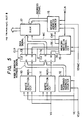
- Fig. 5 is a block diagram of the original recognition circuit 7 shown in Fig. 3.
- a white detection circuit 10 detects a position (the minimum main scanning address) of a white pixel given as the ground color pixel of the original and appearing first in the image signal VD during the valid section of the signal VE, i.e., the main scanning valid image section.
- a white detection circuit 11 detects a position (the maximum main scanning address) of a white pixel given as the ground color pixel of the original and appearing last in the image signal VD during the valid section of the signal VE.
- the white detection circuits 10 and 11 supply detection signals WDT1 and WDT2 to tristate D flip-flops 13 and 14, respectively.
- the flip-flops 13 and 14 Upon reception of the detection signals WDT1 and WDT2, the flip-flops 13 and 14 hold a main scanning address generated by a main scanning address counter 12.
- the main scanning address counter 12 counts up signals VCLK during the valid section of the signal VE from value 0 and outputs a count as the main scanning address signal.
- a memory write-in control circuit 15 generates a control signal for writing the main scanning address data from the D flip-flops 13 and 14 to a random access memory (to be referred to as a RAM hereinafter) 17.
- the memory write-in control circuit 15 uses a write clock signal MCLK during the invalid section of the signal VE and outputs OE1 and OE2 for cotnrolling the outputs from the D flip-flops 13 and 14, a data write signal WE for the RAM 17, a count enable signal CNT for a memory address counter 16, and the like.
- the memory address counter 16 starts the count-up operation from count "0" upon reception of the signal CNT during the invalid section of the signal VSYNC and generates a write address signal for the RAM 17.
- Fig. 6 is a timing chart showing the detailed timings of the original recognition circuit in Fig. 5.
- the original recognition circuit in Fig. 5 is operated during the valid section of the signal VSYNC and sequentially writes the main scanning address data detected for every valid section (i.e., for every main scanning) of the VE signal in the RAM 17 during the memory write period of the invalid section of the signal VE.
- the values of the main scanning address generated by the main scanning address counter 12 are represented by C0, C1, C2, and C3.
- the value C0 is the main scanning address at the start (i.e., the leading edge of the signal VE) of the main scanning section.
- the value C3 is the main scanning address at the end (i.e., the trailing edge of the signal VE) of the main scanning section.
- the count of the main scanning address counter 12 is incremented, the value C0 is always smaller than the value C3, and the values C1 and C2 fall within the range between the values C0 and C3.
- the value C0 is given as value "0" to simplify the circuit arrangement.
- the value C1 represents the minimum main scanning address at the time when the white detection circuit 10 detects the white pixel representing the original ground color
- the value C2 represents the maximum scanning address at the time when the white detection circuit 11 detects the white pixel representing the original ground color.
- the white detection circuit 10 starts detection of the white pixel during the valid section of the signal VE.
- the white detection circuit 10 detects the first white pixel, it outputs a detection signal WDT1, as shown in Fig. 6, so that the detection operation is reset during the invalid section of the signal VE.
- the white detection circuit 11 detects the white pixel during the valid section of the signal VE.
- the white detection circuit 11 Upon detection of the white pixel, the white detection circuit 11 generates a detection signal WDT2. As shown in Fig. 6, the detection operation is reset during the invalid section of the signal VE.
- the D flip-flops 13 and 14 comprise ICs (e.g., standard TTLs 74LS374 available from Texas Instruments, Inc., U.S.A.) for holding data at the leading edge, the values C1 and C2 are respectively held by the D flip-flops 13 and 14 at the end of the valid section of the signal VE.
- ICs e.g., standard TTLs 74LS374 available from Texas Instruments, Inc., U.S.A.
- the value C1 and C2 respectively held by the flip-flops 13 and 14 are written in the RAM 17.
- the flip-flops 13 and 14 are cleared in response to a signal CLR, thereby resetting their values "0" so as not to cause the RAM 17 to receive the white pixel detection value of the previous line when the detection signals WDT1 and WDT2 are not generated, i.e., when the white pixel is not present in the image signal VD.
- the values C1 and C2 are set to be "0".
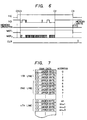
- Fig. 7 shows a memory map of the RAM 17 for storing the values C1 and C2.
- the value C2 is written in units of lines. If the RAM 17 stores 8-bit data and the values C1 and C2 comprise 16-bit signals, respectively, 4-byte data is written for each line. Therefore, the values C1 and C2 of the nth line are writen at addresses (4(n-1))th to (4(n-1)+3)th addresses of the RAM 17, as shown in Fig. 7.
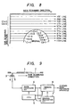
- Fig. 8 is a view showing the correspondence between the data written in the RAM 17 and the actual original position.
- the values C1 and C2 are zero. Since the original image is found from the seventh line, the values C1 and C2 are set to be C1-7 to C1-11 and C2-7 to C2-11 in the RAM 17. By checking the values C1-7 to C1-11 and C2-7 to C2-11, or by checking that the leading end of the original corresponds to the seventh line, the shape (e.g., the original size is indeterminate) of the original can be detected.
- Data stored in the RAM 17 may be used as trimming data without modifications or may be used to access data using a CPU or the like so as to determine the original size and the original position on the table. In the latter case, the data in the RAM 17 can be used for image editing such as automatic magnification change.
- the original position is recognized in units of main scanning lines.
- the original may be recognized for every few lines. In this case, the required memory capacity can be reduced to effectively obtain an inexpensive circuit arrangement.
- a circuit may be added to descriminate the white area only if all pixels are white pixels.
- a simple algorithm for repeating original position detection in units of main scanning lines is used to store the detected position data in the memory, thereby constituting a low-cost original recognition apparatus. Any other figure than a rectangle can be accurately recognized by the data stored in the memory.
- the size, shape, and position of the original placed on the original table can be recognized.
- Various types of image processing such as recording medium selection, image shifting, and image enlargement/reduction can be performed according to the recognition results.
- Fig. 9 is a block diagram of an image reading apparatus with an original recognition function for processing the read-in image signal according to the recognition result.
- the CPU 9 controls the respective blocks in Fig. 9 and is operated in response to an instruction or the like from a scanning unit (not shown).
- Fig. 10 is a block diagram showing the detailed arrangement of the original recognition circuit 7 ⁇ and a trimming circuit 8 in Fig. 9.
- the arrangement receives signals VE, VCLK, SYNC, and VD from an image processing circuit 6 in Fig. 9.
- the arrangement also receives signals DTWR, ACEB and VDOE from the CPU 9.
- a white detection circuit 30 detects a position (the minimum main scanning address) of a white pixel given as the ground color pixel of the original and appearing first in the image signal VD during the valid section of the signal VE, i.e., the main scanning valid image section.
- a white detection circuit 31 detects a position (the maximum main scanning address) of a white pixel given as the ground color pixel of the original and appearing last in the image signal VD during the valid section of the signal VE.
- the white detection circuits 30 and 31 supply detection signals WDT1 and WDT2 to tristate D flip-flops 33 and 34, respectively.
- the flip-flops 33 and 34 hold a main scanning address generated by a main scanning address counter 32.
- the main scanning address counter 32 counts up signals VCLK during the valid section of the signal VE from value 0 and outputs a count as the main scanning address signal. Therefore, the count of the main scanning address counter 32 corresponds to each main scanning pixel position.
- a memory control circuit 35 generates a control signal for writing the main scanning address data from the D flip-flops 33 and 34 to a random access memory (to be referred to as a RAM hereinafter) 37.
- the memory control circuit 35 also supplies a read control signal to the RAM 37.
- the memory control circuit 35 uses a write/read clock signal MCLK during the invalid section of the signal VE and outputs signals OE1 and OE2 for controlling the outputs from the D flip-flops 33 and 34, an output clear signal CLK, a data write signal WE for the RAM 17, a count enable signal CNT for a memory address counter 36, signals DWR1 and DWR2 for causing D flip-flops 40 and 41 to latch the data, and the like.
- the memory address counter 36 starts the count-up operation from count "0" upon reception of the signal CNT during the invalid section of the signal VSYNC and generates a read address signal for the RAM 17.
- the D flip-flops 40 and 41 hold the data read out from the RAM 37 and respectively output data Q1 and data Q2 used for comparison by comparators 42 and 43.
- the comparators 42 and 43 compare data Q1 and data Q2 with the main scanning address signal from the main scanning address counter 32, and generate trimming signals T1 and T2 in cooperation with an inverter 44 and an AND gate 45.
- a JK flip-flops 46 and an AND gate 47 perform trimming of the signal VD in response to the signals T1 and T2.
- a selector 38 and a bus transceiver 39 constitute the CPU (Central Processing Unit) 9 to access the RAM 37.
- the external data write/read access of the RAM 37 can be freely performed.
- the white detection circuits 30 and 31, the D flip-flops 33 and 34, and the main scanning address counter 32 are operated in the same manner as the white detection circuits 10 and 11, D flip-flops 13 and 14, and the main scanning address counter 12 in Fig. 3.
- the same original recognition operation as in Fig. 3 is performed under the control of the main control circuit 35 and the memory address counter 36.
- the circuit in Fig. 10 is operated during the valid section of the signal VSYNC and continuously writes in the RAM 37 main scanning address data C1 and C2 detected for every valid section of the signal VE in the same manner as in Fig. 7.
- Values C1 and C2 detected in units of lines are sequentially written from address 0 of the RAM 37. More specifically, if the RAM 37 stores 8-bit data and the values C1 and C2 comprise 16-bit signals, respectively, 4-byte data is written for each line, as shown in Fig. 7. Therefore, the values C1 and C2 of the nth line are written at addresses (4(n-1))th to (4(n-1)+3)th addresses of the RAM 37.
- Fig. 11 is a timing chart for explaining operation for reading out data from the RAM 37 in Fig. 10.
- the circuit of Fig. 10 is operated during the valid section of the signal VSYNC.
- the main scanning address data read out from the RAM 37 is continuously written in the D flip-flops 40 and 41 during the invalid section of the signal VE.
- Data coincidence signals from the comparators 42 and 43 are converted into trimming signals T1 and T2 by means of the inverter 44 and the AND gate 45.
- the signals T1 and T2 are converted by the JK flip-flop 46 into a signal TRIM.
- the inverter 44 and the AND gate 45 are circuits for inhibiting inversion of the output from the JK flip-flop 46 when the comparators 42 and 43 simultaneously generate the data coincidence signal.
- the identical data signals are respectively set in the comparators 42 and 43 to inhibit the signal TRIM. In other words, image output by the AND gate 47 can be inhibited.
- the comparator 42 Upon detection of the leading edge (i.e., the valid section of the signal VE) of the signal VE, if the comparator 42 detects a coincidence between the main scanning address data written in the D flip-flop 40 and the main scanning count value, the signal T1 is supplied to the JK flip-flop 46, thereby supplying the signal TRIM to the AND gate 47. Therefore, the AND gate 47 generates the signal VD as a signal VDOUT in response to the signal TRIM.
- the comparator 43 detects the coincidence between the main scanning address data written in the D flip-flop 43 and the main scanning count, the signal T2 is supplied to the JK flip-flop 46, thereby interrupting supply of the signal TRIM to the AND gate 47. Therefore, the AND gate 47 is disabled to stop outputting the signal VD.
- Fig. 12 shows an actual read-in image.
- dust such as paper dust on the original table is represented by a
- noise components of the image signal are represented by b and c
- a black portion of the original is represented by d .
- the four corners of the original which correspond to points PK1, PK2, PK3, and PK4 are detected by data stored in the RAM 37.
- Data corresponding to the dust a is eliminated, the noises b and c are converted into black and white noise components with a very low level, and the portion d is converted to be displayed as part of the original under the control of the CPU 9. Trimming is then performed based on the converted data.
- Fig. 13 is a flow chart of original recognition processing and trimming processing under the control of the CPU 9 in Fig. 9.
- step ST10 the signal DTWR in Fig. 10 is enabled (the mode for writing original recognition data in the RAM 37 is designated), the signal ACEB is disabled (inhibition of access for the RAM 37 by the CPU 9 is designated), and the signal VDOE is disabled (the image output inhibition is designated).
- step SP11 an image is input, and original recognition data is written in the RAM 37.
- step SP12 the signal ACEB is disabled (inhibition of access for the RAM under the control of the CPU is designated).
- step SP13 the data written in the RAM 37 is checked, and correction operation described with reference to Fig. 12 is performed by the CPU.
- the trimming data is derived from the original recognition data.
- the original size and its position are detected from the original recognition data, and processing such as recording medium selection and enlargement/reduction ratio setting is performed as needed.
- step SP14 the signal DTWR is disabled (mode for reading out the trimming data from the RAM 37 is designated), the signal ACEB is disabled (inhibition of access for the RAM by the CPU is designated), and the signal VDOE is enabled (image output is designated).
- step SP15 the same image as read in step SP11 is read in, and at the same time, trimming is performed to output the image signal.
- Fig. 14 is a flow chart of the operation when original recognition operation is not performed but only trimming is performed.
- step SP20 the signal ACEB is turned off (inhibition of access for RAM 37 by the CPU is designated).
- step SP21 trimming area designation data entered at the keyboard or digitizer arranged in the operation unit is written in the RAM 37.
- step SP22 the signal DTWR is disabled (mode for reading out trimming data from the RAM 37 is designated), the signal ACEB is disabled (inhibition of access for the RAM 37 by the CPU is designated), and the signal VDOE is enabled (image output is designated).
- step SP23 image subjected to trimming is read in, and trimming is performed. The resultant image signal is then output.
- the original position recognition and trimming are performed in units of main scanning lines. However, if high position control precision is not required, trimming can be performed for every few lines. The required memory capacity of the RAM 37 can be reduced to prepare inexpensive recognition and trimming circuits.
- the original or the original glass table may be moved in place of the reading unit 3 along the subscanning direction.
- the image of a predetermined area may be erased, and the resultant image may be output.
- the present invention is easily applicable to such masking.
- the signal TRIM supplied to the AND gate 47 for gating the image signal is inverted by an inverter, and the inverted signal is supplied to the AND gate 47.
- a simple algorithm for repeating original position detection in units of main scanning lines is used, the detection position data is stored in the memory, and the data is accessed by an arithmetic circuit such as a microcomputer, thereby constituting a low-cost original recognition circuit.
- an arithmetic circuit such as a microcomputer
- the entire area of the original placed on the original table is prescanned once, and the edges of the original are detected for every line or every few lines.
- the detected data is then stored in the RAM, and the image is processed on the basis of the storage data in the RAM.
- the original recognition prescanning is performed prior to reading of the original image.
- Fig. 15 is a block diagram of an image reading apparatus according to still another embodiment of the present invention.
- a line buffer memory 29 is inserted between an image processing circuit 6 and a trimming circuit 8 in Fig. 15, and that a bound detection circuit 27 is used in place of the original recognition circuit 7 of Fig. 3.
- One-line serial image data read by a contact type line image sensor 5 is subjected to predetermined processing such as shading correction and binarized by an image processing circuit 6.
- the binarized image signal is input to the bound detection circuit 7 and the line buffer memory 29 for delaying image data while the bound detection circuit 7 detects the original area.
- the image data delayed by the line buffer memory 29 and the original area detection data from the bound detection circuit 27 are input to the trimming circuit 8 for transferring only the necessary image area excluding unnecessary image area to external image processing equipment.
- the image signal is output from the image processing circuit 6, as described with reference to Fig. 4.
- a signal VE represents a valid section of an image signal VD
- a signal VSYNC represents a subscanning valid section of the image signal VD.
- the signals VE, VSYNC, and VD are output in synchronism with a signal VCLK as a clock signal.
- Fig. 16 is a block diagram showing the detailed arrangement of the bound detection circuit 27, the trimming circuit 8, and the line buffer memory 29.
- the arrangement receives the signals VE, VCLK, and VD from the image processing circuit 6 in Fig. 15.
- a white detection circuit 50 detects a position (the minimum main scanning address) of a white pixel given as the ground color pixel of the original and appearing first in the image signal VD during the valid section of the signal VE, i.e., the main scanning valid image section.
- a white detection circuit 51 detects a position (the maximum main scanning address) of a white pixel given as the ground color pixel of the original and appearing last in the image signal VD during the valid section of the signal VE.
- the white detection circuits 30 and 31 supply detection signals WDT1 and WDT2 to tristate D flip-flops 53 and 54, respectively. Upon reception of the detection signals WDT1 and WDT2, the flip-flops 53 and 54 hold a main scanning address generated by a main scanning address counter 52.
- the main scanning address counter 32 counts up signals VCLK during the valid section of the signal VE from value 0 and outputs a count as the main scanning address signal. Therefore, the count of the main scanning address counter 52 corresponds to each main scanning pixel position.
- D flip-flops 55 and 56 are circuits for temporarily storing the main scanning address data held by the D flip-flops 53 and 54.
- the main scanning address data held by the flip-flops 55 and 56 is input to comparators 57 and 58 and compared with the main scanning address signal.
- Each of the comparators 57 and 58 compares inputs A and B. If the input A coincides with the input B, a coincidence signal is output from each comparator.
- the coincidence signals from the comparators 57 and 58 are used for generating a signal TRIM for trimming the image signal by means of an inverter 59, and AND gate 60, and a JK flip-flop 61.
- a line buffer memory 63 is a memory for delaying the image data.
- the memory 63 must have a memory capacity for delaying the data by a one-line time for detecting the original area.
- the image data signal VD ⁇ delayed by the line buffer memory 63 is logically ORed with the AND gate 62, thus outputting image data VDOUT.
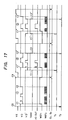
- Fig. 17 is a timing chart showing the operation timings of the circuit of Fig. 16.
- the main scanning addresses from the main scanning address counter 52 have values C0, C1, C1 ⁇ , C1", C2, C2 ⁇ , and C2", and C3.
- the value C0 represents the main scanning address at the start of the main scanning valid section.
- the value C3 represents the main scanning address at the end of the main scanning valid section.
- the value C0 is smaller than the value C3.
- the values C1, C1 ⁇ , C1", C2, C2 ⁇ , and C2" fall within the range of the values C0 and C3.
- the value C0 is set to be "0" to simplify the circuit arrangement.
- the values C1, C1 ⁇ and C1" are minimum main scanning addresses of the white pixels as the original ground color, which are detected by the white detection circuit 50.
- the values C2, C2 ⁇ , and C2" are maximum main scanning addresses of the white pixels as the original ground color, which are detected by the white detection circuit 51.
- the white detection circuit 50 detects the white pixel during the valid section of the signal VE. Upon detection of the first white pixel, the white detection circuit 50 outputs the detection signal WDT1, as shown in Fig. 17. The detection circuit 50 is reset during the invalid section of the signal VE. Similarly, the white detection circuit 51 starts detection of the white pixels during the valid section of the signal VE. Upon detection of the white pixel, the detection circuit 51 outputs the detection signal WDT2, as shown in Fig. 17. The circuit 51 is then reset during the invalid section of the signal VE.
- D flip-flops 53 and 54 comprise ICs (e.g., standard TTLs 74LS273 available from Texas Instruments, Inc) for holding data at the leading edge, the values C1, C1 ⁇ , and C1" and the values C2, C2 ⁇ , and C2" are respectively held in the flip-flops 53 and 54 at the end of the valid section of the signal VE.
- ICs e.g., standard TTLs 74LS273 available from Texas Instruments, Inc
- An inverter 64 is a circuit for holding data at the trailing edge of the signal VE when the D flip-flops 55 and 56 comprise TTLs 74LS273.
- the D flip-flops 53 and 54 are cleared to zero in response to the signal VE due to the following reason.
- the value of the previous line is not written if the detection signals WDT1 and WDT2 are not generated, i.e., if the white pixel is not present in the image signal VD.
- values C1, C1 ⁇ , C1", C2, C2 ⁇ , and C2" are set to be zero.
- the one-line delayed data VD subjected to the detection of the original area that is, the image data VD ⁇ is trimmed.
- the coincidence signals from the comparators 57 and 58 are connected as the signals T1 and T2 to the J and K inputs of the JK flip-flop 61.
- the JK flip-flop 61 is normally cleared during the invalid section of the signal VE and generates the signal TRIM representing the original area during the valid section of the signal VE.
- the inverter 59 and the AND gate 60 serve to prevent generation of the signal TRIM under the condition that both the values C1 and C2 are an identical value, e.g., zero.
- the signal TRIM and the signal VD ⁇ are logically ORed by the AND gate 62 so that the signal VD ⁇ corresponding to the logic "1" period of the signal TRIM is output as image data VDOUT.
- Fig. 18 shows an example of input image data read by the contact type line image sensor 5 of Fig. 15. This example assumes the case wherein an original is manually cut and copied. As is apparent from Fig. 18, the boundary is cut in a zigzag manner, and the portion excluding the original area is a black image.
- Fig. 19 shows output image data when the image data of Fig. 18 is input to the circuit of Fig. 16.
- the original area is trimmed in units of lines, and the hatched portion (i.e., a nonoriginal area) in Fig. 18 is output as a white image of Fig. 19. It is thus apparent that the background image is clearly removed.
- the image area is recognized and trimmed in units of main scanning lines.
- recognition operation can be made for every few lines.
- the buffer memory 63 has a memory capacity of a few lines, and the recognized area data of a few lines is stored therein.
- the memory capacity of the buffer memory 63 may be set to delay the image data so as to correspond to the operating time of the bound detection circuit 27.
- a circuit may be added to determine a white area if a plurality of succeeding pixels are all white pixels.
- the original to be read or the original glass table may be scanned along the subscanning direction.
- a simple algorithm is used to repeat boundary detection of the original and background images in units of main scanning lines, and the detection position data is used to extract the image signal, so that unnecessary background image can be eliminated from the image data at high speed without performing prescanning and trimming of a figure other than a rectangle can be accurately performed.
Landscapes
- Engineering & Computer Science (AREA)
- Multimedia (AREA)
- Signal Processing (AREA)
- Editing Of Facsimile Originals (AREA)
- Facsimile Scanning Arrangements (AREA)
Claims (8)
einer Einrichtung (3-6) zur Eingabe von Bildsignalen, die Vorlagen- und Nicht-Vorlagenbereiche darstellen;
einer Einrichtung (20, 51) zur Erfassung eines Bildsignals, das aus den mittels der Eingabeeinrichtung eingegebenen Bildsignalen den Vorlagenbereich darstellt;
einer Einrichtung (8, 57-62) , dia auf der Basis eines Erfassungsergebnisses der Erfassungseinrichtung aus dem Bildsignal ein dem Vorlagenbereich entsprechendes Bildsignal extrahiert; dadurch gekennzeichnet, daß [a] eine Einrichtung (52-56) vorgesehen ist, die in Übereinstimmung mit dem Erfassungsergebnis der Erfassungseinrichtung jeweils für n abgetastete Zeilen den Vorlagenbereich darstellende Bereichsdaten zwischenspeichert und den Vorlagenbereich darstellende Bereichsdaten erzeugt, wobei n eine positive ganze Zahl ist;
[b] eine Einrichtung (29, 63) zur Verzögerung der mittels der Eingabeeinrichtung eingegebenen Bildsignale vorgesehen ist; und daß
[c] die Extraktionseinrichtung auf der Grundlage der verzögerten Bildsignale in Übereinstimmung mit den von der zwischenspeichereinrichtung (52-56) erzeugten Bereichsdaten arbeitet.
Applications Claiming Priority (6)
| Application Number | Priority Date | Filing Date | Title |
|---|---|---|---|
| JP60217231A JPS6276962A (ja) | 1985-09-30 | 1985-09-30 | 原稿認識装置 |
| JP217231/85 | 1985-09-30 | ||
| JP60286693A JPS62144462A (ja) | 1985-12-19 | 1985-12-19 | 画像信号処理装置 |
| JP286693/85 | 1985-12-19 | ||
| JP286695/85 | 1985-12-19 | ||
| JP60286695A JPS62144464A (ja) | 1985-12-19 | 1985-12-19 | 画像信号処理装置 |
Publications (3)
| Publication Number | Publication Date |
|---|---|
| EP0218447A2 EP0218447A2 (de) | 1987-04-15 |
| EP0218447A3 EP0218447A3 (en) | 1988-08-24 |
| EP0218447B1 true EP0218447B1 (de) | 1991-02-06 |
Family
ID=27330002
Family Applications (1)
| Application Number | Title | Priority Date | Filing Date |
|---|---|---|---|
| EP86307488A Expired EP0218447B1 (de) | 1985-09-30 | 1986-09-30 | Bildsignalverarbeitungsvorrichtung |
Country Status (3)
| Country | Link |
|---|---|
| US (1) | US4870500A (de) |
| EP (1) | EP0218447B1 (de) |
| DE (1) | DE3677449D1 (de) |
Families Citing this family (21)
| Publication number | Priority date | Publication date | Assignee | Title |
|---|---|---|---|---|
| US4833722A (en) * | 1987-07-24 | 1989-05-23 | Eastman Kodak Company | Apparatus and methods for locating edges and document boundaries in video scan lines |
| JP2578448B2 (ja) * | 1987-11-28 | 1997-02-05 | キヤノン株式会社 | 画像処理装置 |
| US5040078A (en) * | 1988-07-15 | 1991-08-13 | Canon Kabushiki Kaisha | Image processing apparatus displaying boundaries of an original image |
| US5179454A (en) * | 1988-09-12 | 1993-01-12 | Canon Kabushiki Kaisha | Image reading apparatus |
| US5189523A (en) * | 1989-11-27 | 1993-02-23 | Canon Kabushiki Kaisha | Image processing apparatus |
| JPH03230683A (ja) * | 1990-02-05 | 1991-10-14 | Konica Corp | 複写機 |
| EP0453395B1 (de) * | 1990-03-29 | 1995-11-02 | Ciba-Geigy Ag | Druckempfindliches Aufzeichnungsmaterial |
| US5124537A (en) * | 1990-10-29 | 1992-06-23 | Omniplanar, Inc. | Omnidirectional bar code reader using virtual scan of video raster scan memory |
| JP3225112B2 (ja) * | 1992-09-25 | 2001-11-05 | 株式会社東芝 | 原稿読取装置と原稿読取方法 |
| JPH077606A (ja) * | 1993-04-20 | 1995-01-10 | Nikon Corp | 画像読取装置 |
| US5565432A (en) * | 1994-11-07 | 1996-10-15 | American Home Products Corporation | Smooth muscle cell proliferation inhibitors |
| US5970183A (en) * | 1995-12-26 | 1999-10-19 | Canon Kabushiki Kaisha | Detecting an outer shape of an original image and controlling to inhibit image frame processing in accordance with the detection result |
| JPH09197549A (ja) * | 1996-01-17 | 1997-07-31 | Fuji Photo Film Co Ltd | マイクロフィルムスキャナの制御方法 |
| FR2785629B1 (fr) * | 1998-11-10 | 2000-12-22 | Coatex Sa | Composition polymerique retenteur d'eau et activateur d'azurants optiques, sauces de couchage pour papier, et feuilles de papier couche ainsi obtenues |
| JP3829667B2 (ja) * | 2001-08-21 | 2006-10-04 | コニカミノルタホールディングス株式会社 | 画像処理装置、画像処理方法、画像処理方法実行のためのプログラム及びプログラムを記憶した記憶媒体 |
| US7742198B2 (en) * | 2001-09-12 | 2010-06-22 | Seiko Epson Corporation | Image processing apparatus and method |
| US7059785B2 (en) | 2001-09-12 | 2006-06-13 | Seiko Epson Corporation | Composite printer and scan image copying method |
| JP3932379B2 (ja) * | 2001-10-02 | 2007-06-20 | 株式会社日立製作所 | 画像処理装置と撮像素子 |
| US7015401B2 (en) * | 2001-11-23 | 2006-03-21 | Aiptek International, Inc. | Image processing system with handwriting input function and the method for forming the same |
| KR100947002B1 (ko) * | 2005-08-25 | 2010-03-11 | 가부시키가이샤 리코 | 화상 처리 방법 및 장치, 디지털 카메라, 및 화상 처리프로그램을 기록한 기록 매체 |
| US8098936B2 (en) | 2007-01-12 | 2012-01-17 | Seiko Epson Corporation | Method and apparatus for detecting objects in an image |
Family Cites Families (10)
| Publication number | Priority date | Publication date | Assignee | Title |
|---|---|---|---|---|
| DE122456C (de) * | ||||
| US4325086A (en) * | 1979-04-20 | 1982-04-13 | Canon Kabushiki Kaisha | Recording device |
| US4439790A (en) * | 1981-01-23 | 1984-03-27 | Canon Kabushiki Kaisha | Image forming apparatus |
| JPS58142487A (ja) * | 1982-02-18 | 1983-08-24 | Fuji Electric Co Ltd | 特徴抽出装置 |
| DE3314116A1 (de) * | 1983-04-19 | 1984-10-25 | Dr.-Ing. Rudolf Hell Gmbh, 2300 Kiel | Verfahren und vorrichtung zum bestimmen des bildausschnittes von vorlagen fuer die reproduktion in der drucktechnik |
| JPS59224976A (ja) | 1983-06-03 | 1984-12-17 | Nec Corp | 写真電送装置 |
| JPS6052156A (ja) * | 1983-09-01 | 1985-03-25 | Canon Inc | 画像処理装置 |
| JPH0626423B2 (ja) * | 1983-12-08 | 1994-04-06 | キヤノン株式会社 | 原稿読取り装置 |
| JPS60124173A (ja) * | 1983-12-09 | 1985-07-03 | Canon Inc | 画像処理装置 |
| JPS62224976A (ja) * | 1986-03-27 | 1987-10-02 | Toshiba Corp | 薄膜トランジスタ |
-
1986
- 1986-09-25 US US06/911,416 patent/US4870500A/en not_active Expired - Lifetime
- 1986-09-30 DE DE8686307488T patent/DE3677449D1/de not_active Expired - Lifetime
- 1986-09-30 EP EP86307488A patent/EP0218447B1/de not_active Expired
Also Published As
| Publication number | Publication date |
|---|---|
| US4870500A (en) | 1989-09-26 |
| DE3677449D1 (de) | 1991-03-14 |
| EP0218447A3 (en) | 1988-08-24 |
| EP0218447A2 (de) | 1987-04-15 |
Similar Documents
| Publication | Publication Date | Title |
|---|---|---|
| EP0218447B1 (de) | Bildsignalverarbeitungsvorrichtung | |
| US4899227A (en) | Image processing apparatus detecting the size or position of an information portion of an original | |
| JPH0737892B2 (ja) | パターン欠陥検査方法 | |
| US5483606A (en) | Method for automatically registering a document having a plurality of pages | |
| JP2828645B2 (ja) | マーク領域判定装置 | |
| US5371610A (en) | Image data processing apparatus | |
| GB2194117A (en) | Image processing apparatus | |
| US5282064A (en) | Apparatus for simultaneous reading of reflective and light conductive portions of an original | |
| US5606656A (en) | Image data processing unit for forming a plurality of identical images in a single output image area | |
| JPS62144462A (ja) | 画像信号処理装置 | |
| US5299030A (en) | Image data processing method and apparatus with mixture of simple binarization and psuedo intermediate tone | |
| JPH02253377A (ja) | 画像編集装置 | |
| JPS6276962A (ja) | 原稿認識装置 | |
| JPS62144464A (ja) | 画像信号処理装置 | |
| JP2903214B2 (ja) | 領域指定装置 | |
| JP3203024B2 (ja) | 画像処理装置及び画像処理方法 | |
| KR100271158B1 (ko) | 다중 데이터 버스를 이용한 고속 화상 이치화 장치 및 방법 | |
| JP2547748B2 (ja) | 画像処理装置 | |
| JP2921685B2 (ja) | 画データ補正装置 | |
| JP2985303B2 (ja) | 記録装置の領域認識方式 | |
| JPS62144463A (ja) | 画像信号処理装置 | |
| JPH0750504B2 (ja) | パタ−ン認識装置 | |
| JPS6346872A (ja) | 画像処理装置 | |
| JP2926710B2 (ja) | 画像処理装置 | |
| JP2755506B2 (ja) | 画像形成装置 |
Legal Events
| Date | Code | Title | Description |
|---|---|---|---|
| PUAI | Public reference made under article 153(3) epc to a published international application that has entered the european phase |
Free format text: ORIGINAL CODE: 0009012 |
|
| AK | Designated contracting states |
Kind code of ref document: A2 Designated state(s): DE FR GB IT NL |
|
| PUAL | Search report despatched |
Free format text: ORIGINAL CODE: 0009013 |
|
| AK | Designated contracting states |
Kind code of ref document: A3 Designated state(s): DE FR GB IT NL |
|
| 17P | Request for examination filed |
Effective date: 19890114 |
|
| 17Q | First examination report despatched |
Effective date: 19890522 |
|
| GRAA | (expected) grant |
Free format text: ORIGINAL CODE: 0009210 |
|
| AK | Designated contracting states |
Kind code of ref document: B1 Designated state(s): DE FR GB IT NL |
|
| REF | Corresponds to: |
Ref document number: 3677449 Country of ref document: DE Date of ref document: 19910314 |
|
| ITF | It: translation for a ep patent filed | ||
| ET | Fr: translation filed | ||
| PLBE | No opposition filed within time limit |
Free format text: ORIGINAL CODE: 0009261 |
|
| STAA | Information on the status of an ep patent application or granted ep patent |
Free format text: STATUS: NO OPPOSITION FILED WITHIN TIME LIMIT |
|
| 26N | No opposition filed | ||
| REG | Reference to a national code |
Ref country code: GB Ref legal event code: IF02 |
|
| PGFP | Annual fee paid to national office [announced via postgrant information from national office to epo] |
Ref country code: FR Payment date: 20050914 Year of fee payment: 20 |
|
| PGFP | Annual fee paid to national office [announced via postgrant information from national office to epo] |
Ref country code: NL Payment date: 20050915 Year of fee payment: 20 |
|
| PGFP | Annual fee paid to national office [announced via postgrant information from national office to epo] |
Ref country code: GB Payment date: 20050916 Year of fee payment: 20 |
|
| PGFP | Annual fee paid to national office [announced via postgrant information from national office to epo] |
Ref country code: IT Payment date: 20050917 Year of fee payment: 20 |
|
| PGFP | Annual fee paid to national office [announced via postgrant information from national office to epo] |
Ref country code: DE Payment date: 20051118 Year of fee payment: 20 |
|
| PG25 | Lapsed in a contracting state [announced via postgrant information from national office to epo] |
Ref country code: GB Free format text: LAPSE BECAUSE OF EXPIRATION OF PROTECTION Effective date: 20060929 |
|
| PG25 | Lapsed in a contracting state [announced via postgrant information from national office to epo] |
Ref country code: NL Free format text: LAPSE BECAUSE OF EXPIRATION OF PROTECTION Effective date: 20060930 |
|
| REG | Reference to a national code |
Ref country code: GB Ref legal event code: PE20 |
|
| NLV7 | Nl: ceased due to reaching the maximum lifetime of a patent |
Effective date: 20060930 |