EP0219241A2 - Nichtflüchtiger Halbleiterspeicher - Google Patents
Nichtflüchtiger Halbleiterspeicher Download PDFInfo
- Publication number
- EP0219241A2 EP0219241A2 EP86307290A EP86307290A EP0219241A2 EP 0219241 A2 EP0219241 A2 EP 0219241A2 EP 86307290 A EP86307290 A EP 86307290A EP 86307290 A EP86307290 A EP 86307290A EP 0219241 A2 EP0219241 A2 EP 0219241A2
- Authority
- EP
- European Patent Office
- Prior art keywords
- insulator film
- gate electrode
- floating gate
- film
- cvd
- Prior art date
- Legal status (The legal status is an assumption and is not a legal conclusion. Google has not performed a legal analysis and makes no representation as to the accuracy of the status listed.)
- Withdrawn
Links
Images


Classifications
-
- H—ELECTRICITY
- H10—SEMICONDUCTOR DEVICES; ELECTRIC SOLID-STATE DEVICES NOT OTHERWISE PROVIDED FOR
- H10D—INORGANIC ELECTRIC SEMICONDUCTOR DEVICES
- H10D30/00—Field-effect transistors [FET]
- H10D30/60—Insulated-gate field-effect transistors [IGFET]
- H10D30/68—Floating-gate IGFETs
- H10D30/681—Floating-gate IGFETs having only two programming levels
- H10D30/683—Floating-gate IGFETs having only two programming levels programmed by tunnelling of carriers, e.g. Fowler-Nordheim tunnelling
Definitions
- This invention relates to non-volatile semiconductor memories.
- EEPROM floating gate type erasable and programmable non-volatile semiconductor memory
- Figure 2 is a sectional view of a conventional floating gate type EEPROM.
- an N+-type source region 12 On the surface of a P-type semiconductor substrate 11, there are provided an N+-type source region 12 and a drain region 13, above which is provided a gate oxidised film 14.
- a thin oxidised film 15 In a small area adjacent to the drain region 13, there is provided a thin oxidised film 15, above which is provided a floating gate electrode 16, a second gate oxidised film 17 and a control gate electrode 18.
- a writing operation is conducted by applying a writing voltage to the control gate electrode 18, so that electrons are injected from thedrain region 13 into the floating gate electrode 16 through the thin oxidised film 15.
- An erasing operation is conducted by applying an erasing voltage to the control gate electrode 18, so that electrons are emitted from the floating gate electrode 16 into the drain region 13 through the thin oxidised film 15.
- This floating gate type EEPROM are effected by means of a Fowler-Nordheim tunnel current through a thin oxidised film (100 to 150 ⁇ ).
- This thin oxide film for writing and erasing operations has heretofore been constituted by a thermally oxidised film.
- the thermally oxidised film 15 conventionally employed for writing and erasing has, however, the disadvantage that breakdown occurs after about 104 writing and erasing operations.
- the present invention employs a CVD insulator film for writing and erasing operations in place of a thermally oxidised film. It has heretofore been considered that a CVD insulator film is inferior to a thermally oxidised film in terms of characteristics, e.g., lower density and large leakage current. However, it has been found that a CVD oxide film which is formed at a high temperature, i.e., 700°C or higher, has superior characteristics to those of a thermally oxidised film.
- Such a CVD insulator film exhibits excellent characteristics when used as a thin film region of the order of 100 ⁇ , that is, the CVD insulator film has a large breakdown current density and is not readily broken down in contrast to the thermally oxidised film.
- the present invention employs a CVD insulator film as a tunnel insulator film.
- a non-volatile semiconductor memory comprising: source and drain regions respectively provided on a semiconductor substrate of one conductivity type opposite to that of the source and drain regions; a gate insulator film provided on the surface of a portion of said substrate which is located between said source and drain regions; a floating gate electrode provided on part of said gate insulator film; and a tunnel insulator film aubbed against the other part of said floating gate electrode and constituting a CVD insulator film, characterised by an electrode for transferring electric charge between the same and said floating gate electrode, provided opposite to said floating gate electrode through said tunnel insulator film; and a control gate electrode provided above said floating gate electrode through an insulator film.
- said CVD insulator film is consituted by a CVD silicon oxide film formed at a temperature less than 700°C.
- said drain region also serves as said electrode which transfers electric charge between the same and said floating gate electrode.
- FIG. 1 there is shown a non-volatile semiconductor memory or floating gate type EEPROM according to the present invention.
- N+-type source and drain regions 2,3 are formed, and a gate oxide film 4 is provided thereon.
- a CVD insulator film 5 of 100 ⁇ thickness is provided on a small region in the vicinity of the drain region, and a floating gate electrode 6, a second gate oxide film 7 and a control gate electrode 8 are provided in that order on the CVD insulator film 5.
- a writing operation is conducted by applying a writing voltage to the control gate electrode 8, so that electrons are injected from the drain region 3 into the floating gate electrode 6 through the CVD insulating film 5.
- An erasing operation is conducted by applying an erasing voltage to the control gate electrode 8, so that electrons are emitted from the floating gate electrode 6 into the drain region 3 through the CVD insulator film 5.
- the CVD insulator film 5 is formed using dichlorosilane (SiH2Cl2) and nitrousoxide (N2O) and a film is formed under a vacuum and at a temperature of 700 to 900°C.
- This CVD insulator film 5 exhibits excellent characteristics when of a thickness of the order of 100 ⁇ . That is, it has a large breakdown current density and is not readily broken down in contrast to the thermally oxidised film 15 of the conventional floating gate type EEPROM. It is therefore possible greatly to increase the number of possible writing and erasing operations.
- CVD oxide film is employed as the CVD insulator film 5
- chemical vapour deposition process is not the only one that can be used.
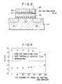
- Figure 4 shows the respective rewriting characteristics of the floating gate type EEPROM of Figure 1 which employs the CVD insulator film 5 and the conventional EEPROM of Figure 2 which employs a thermally oxidised film.
- the number of possible writing and erasing operations is plotted along the abscissa and the threshold value (V TH ) is plotted along the ordinate.
- the EEPROM of Figure 1 which employs the CVD insulator film 5 is relatively durable and breaks down after about 106 writing and erasing operations
- the conventional EEPROM which employs the thermally oxidised film 15 breaks down after about 104 writing and erasing operations.
- the EEPROM of Figure 1 has less change in the threshold value and therefore exhibits high reliability.
- Figure 5 shows the respective breakdown current densities of the CVD insulator film 5 and the thermally oxidised film 15.
- the thickness of the oxide film is plotted along the abscissa and a breakdown current density is plotted along the ordinate.
- the marks shown are as follows: ⁇ Vietnamese breakdown current (A) of the CVD insulator film 5 when the gate voltage V g is positive; ⁇ Vietnamese breakdown current (B) of the CVD insulator film 5 when the gate voltage V g is negative; ⁇ owing breakdown current (C) of the thermally oxidised film 15 when the gate voltage V g is positive; ⁇ bib breakdown current (D) of the thermally oxidised film 15 when the gate voltage V g is negative.
- the CVD insulator film 5 exhibits a larger breakdown current density than that of the thermally oxidised film 15. Accordingly, the CVD insulator film 5 enables the number of writing and erasing operations to be increased by a large margin in contrast to the thermally oxidised film 15.
- Figure 3 is a sectional view of a non-volatile semiconductor memory or floating gate type EEPROM according to a second embodiment of the present invention.
- N+-type source and drain regions 22,23 are formed, and a gate oxide film 24 and a floating gate electrode 26 are provided thereon.
- a second gate oxide film 27 and a control gate electrode 28 are provided on the left-hand portion of the floating gate electrode 26, while a CVD insulator film 25 of 100 ⁇ thickness and a writing and erasing electrode 29 are provided on the right-hand portion of the floating gate electrode 26, the electrode 29 being adapted to transfer electric charge between the same and the floating gate electrode 26.
- a writing operation is conducted by applying a writing voltage to the control gate electrode 28 opposite to that of the electrode 29, so that electrons are injected from the electrode 29 into the floating gate electrode 26 through the CVD insulator film 25.
- An erasing operation is conducted by applying an erasing voltage to the control gate electrode 28, so that electrons are emitted from the floating gate electrode 26 into the electrode 29 through the CVD insulator film 25.
- the floating gate electrode 26 below the CVD insulator film 25 may be formed of polycrystalline silicon. Similar to the embodiment of Figure 1, the CVD insulator film 25 also enables the possible number of writing and erasing operations to be increased by a large margin as compared with the conventional EEPROM of Figure 2 which employs a thermally oxidised film.
- the non-volatile semiconductor memory according to the present invention and described above employs a CVD insulator film 5 as a tunnel oxide film and thereby offers the advantage that the number of possible writing and erasing operations can be increased to about 100 times that of conventional floating gate EEPROMs which employ a thermally oxidised film. Accordingly, the present invention can provide a highly reliable floating gate type EEPROM.
Landscapes
- Non-Volatile Memory (AREA)
Applications Claiming Priority (2)
| Application Number | Priority Date | Filing Date | Title |
|---|---|---|---|
| JP230184/85 | 1985-10-16 | ||
| JP60230184A JPS6289364A (ja) | 1985-10-16 | 1985-10-16 | 不揮発性半導体記憶装置 |
Publications (2)
| Publication Number | Publication Date |
|---|---|
| EP0219241A2 true EP0219241A2 (de) | 1987-04-22 |
| EP0219241A3 EP0219241A3 (de) | 1988-08-24 |
Family
ID=16903913
Family Applications (1)
| Application Number | Title | Priority Date | Filing Date |
|---|---|---|---|
| EP86307290A Withdrawn EP0219241A3 (de) | 1985-10-16 | 1986-09-23 | Nichtflüchtiger Halbleiterspeicher |
Country Status (3)
| Country | Link |
|---|---|
| US (1) | US5122847A (de) |
| EP (1) | EP0219241A3 (de) |
| JP (1) | JPS6289364A (de) |
Cited By (7)
| Publication number | Priority date | Publication date | Assignee | Title |
|---|---|---|---|---|
| EP0294989A3 (de) * | 1987-06-12 | 1990-01-17 | Seiko Instruments Inc. | Nichtflüchtige Halbleiterspeicheranordnung |
| EP0298430A3 (de) * | 1987-07-08 | 1990-05-16 | Hitachi, Ltd. | Halbleiter Anordnung mit schwimmender Gate |
| US5095344A (en) * | 1988-06-08 | 1992-03-10 | Eliyahou Harari | Highly compact eprom and flash eeprom devices |
| US5168465A (en) * | 1988-06-08 | 1992-12-01 | Eliyahou Harari | Highly compact EPROM and flash EEPROM devices |
| US5198380A (en) * | 1988-06-08 | 1993-03-30 | Sundisk Corporation | Method of highly compact EPROM and flash EEPROM devices |
| US5739568A (en) * | 1994-11-28 | 1998-04-14 | Motorola, Inc. | Non-volatile memory having a cell applying to multi-bit data by double layered floating gate architecture and programming method for the same |
| EP2423247A1 (de) | 2010-08-30 | 2012-02-29 | Rhein Chemie Rheinau GmbH | Neuartige wässrige Resorcin-Formaldehyd-Latex-Dispersionen, ein Verfahren zu deren Herstellung und deren Verwendung |
Families Citing this family (7)
| Publication number | Priority date | Publication date | Assignee | Title |
|---|---|---|---|---|
| JP2927794B2 (ja) * | 1988-03-04 | 1999-07-28 | 富士通株式会社 | 半導体記憶装置及びその書込方法 |
| JPH01289282A (ja) * | 1988-05-17 | 1989-11-21 | Ricoh Co Ltd | 半導体記憶装置 |
| JP3805825B2 (ja) * | 1995-09-19 | 2006-08-09 | 株式会社東芝 | 絶縁膜の形成方法 |
| US5869370A (en) * | 1997-12-29 | 1999-02-09 | Taiwan Semiconductor Manufacturing Company Ltd. | Ultra thin tunneling oxide using buffer CVD to improve edge thinning |
| TW454354B (en) * | 1998-07-22 | 2001-09-11 | Winbond Electronics Corp | Improved structure of nonvolatile memory and the manufacturing process thereof |
| US6884295B2 (en) | 2000-05-29 | 2005-04-26 | Tokyo Electron Limited | Method of forming oxynitride film or the like and system for carrying out the same |
| KR100415518B1 (ko) * | 2000-06-30 | 2004-01-31 | 주식회사 하이닉스반도체 | 플래쉬 메모리 셀의 제조 방법 |
Family Cites Families (8)
| Publication number | Priority date | Publication date | Assignee | Title |
|---|---|---|---|---|
| US4002512A (en) * | 1974-09-16 | 1977-01-11 | Western Electric Company, Inc. | Method of forming silicon dioxide |
| US4288256A (en) * | 1977-12-23 | 1981-09-08 | International Business Machines Corporation | Method of making FET containing stacked gates |
| US4274012A (en) * | 1979-01-24 | 1981-06-16 | Xicor, Inc. | Substrate coupled floating gate memory cell |
| DE2916884C3 (de) * | 1979-04-26 | 1981-12-10 | Deutsche Itt Industries Gmbh, 7800 Freiburg | Programmierbare Halbleiterspeicherzelle |
| DE3007892C2 (de) * | 1980-03-01 | 1982-06-09 | Deutsche Itt Industries Gmbh, 7800 Freiburg | Floating-Gate-Speicherzelle |
| US4535349A (en) * | 1981-12-31 | 1985-08-13 | International Business Machines Corporation | Non-volatile memory cell using a crystalline storage element with capacitively coupled sensing |
| US4688078A (en) * | 1982-09-30 | 1987-08-18 | Ning Hseih | Partially relaxable composite dielectric structure |
| CA1204862A (en) * | 1982-09-30 | 1986-05-20 | Ning Hsieh | Programmable read only memory |
-
1985
- 1985-10-16 JP JP60230184A patent/JPS6289364A/ja active Pending
-
1986
- 1986-09-23 EP EP86307290A patent/EP0219241A3/de not_active Withdrawn
-
1988
- 1988-09-07 US US07/241,752 patent/US5122847A/en not_active Expired - Lifetime
Cited By (7)
| Publication number | Priority date | Publication date | Assignee | Title |
|---|---|---|---|---|
| EP0294989A3 (de) * | 1987-06-12 | 1990-01-17 | Seiko Instruments Inc. | Nichtflüchtige Halbleiterspeicheranordnung |
| EP0298430A3 (de) * | 1987-07-08 | 1990-05-16 | Hitachi, Ltd. | Halbleiter Anordnung mit schwimmender Gate |
| US5095344A (en) * | 1988-06-08 | 1992-03-10 | Eliyahou Harari | Highly compact eprom and flash eeprom devices |
| US5168465A (en) * | 1988-06-08 | 1992-12-01 | Eliyahou Harari | Highly compact EPROM and flash EEPROM devices |
| US5198380A (en) * | 1988-06-08 | 1993-03-30 | Sundisk Corporation | Method of highly compact EPROM and flash EEPROM devices |
| US5739568A (en) * | 1994-11-28 | 1998-04-14 | Motorola, Inc. | Non-volatile memory having a cell applying to multi-bit data by double layered floating gate architecture and programming method for the same |
| EP2423247A1 (de) | 2010-08-30 | 2012-02-29 | Rhein Chemie Rheinau GmbH | Neuartige wässrige Resorcin-Formaldehyd-Latex-Dispersionen, ein Verfahren zu deren Herstellung und deren Verwendung |
Also Published As
| Publication number | Publication date |
|---|---|
| JPS6289364A (ja) | 1987-04-23 |
| US5122847A (en) | 1992-06-16 |
| EP0219241A3 (de) | 1988-08-24 |
Similar Documents
| Publication | Publication Date | Title |
|---|---|---|
| JP3710082B2 (ja) | メモリ・トランジスタを作成する方法 | |
| KR100372328B1 (ko) | 반도체저장장치 | |
| USRE31734E (en) | Moderate field hole and electron injection from one interface of MIM or MIS structures | |
| US6753569B2 (en) | Method to fabricate a non-smiling effect structure in split-gate flash with self-aligned isolation | |
| EP0047153B1 (de) | Halbleiterspeicher | |
| EP0219241A2 (de) | Nichtflüchtiger Halbleiterspeicher | |
| EP0062460B1 (de) | Elektrisch löschbare, nicht-flüchtige Halbleiterspeicherelemente | |
| US5789297A (en) | Method of making EEPROM cell device with polyspacer floating gate | |
| US5729496A (en) | Nonvolatile semiconductor memory element and method for fabricating the same | |
| US6326660B1 (en) | Method to improve the capacity of data retention and increase the coupling ratio of source to floating gate in split-gate flash | |
| US4257056A (en) | Electrically erasable read only memory | |
| EP0120303A2 (de) | Halbleiterspeichervorrichtung mit schwebender Torelektrode | |
| EP0228761B1 (de) | Nichtflüchtiger Halbleiterspeicher | |
| JPH05235368A (ja) | データ消去方法 | |
| US5643812A (en) | Method of making EEPROM flash memory cell with erase gate | |
| GB2107119A (en) | A non-volatile semiconductor memory device | |
| EP0443515B1 (de) | Nichtflüchtige Halbleitervorrichtung | |
| KR0124629B1 (ko) | 불휘발성 반도체 메모리장치의 제조방법 | |
| US5371704A (en) | Nonvolatile memory device with compensation for over-erasing operation | |
| EP0481392B1 (de) | Nichtflüchtige Halbleiterspeicheranordnung | |
| US5332915A (en) | Semiconductor memory apparatus | |
| EP0399527A2 (de) | Nichtflüchtige Halbleiter-Speichereinrichtung | |
| JP4969748B2 (ja) | 不揮発性半導体記憶装置デバイス及び不揮発性記憶装置セルの製造方法 | |
| EP0590319B1 (de) | Nichtflüchtige Speicherzelle | |
| US6878984B2 (en) | Non-volatile flash memory having a specific difference between source/floating gate and drain/floating gate overlapped portions |
Legal Events
| Date | Code | Title | Description |
|---|---|---|---|
| PUAI | Public reference made under article 153(3) epc to a published international application that has entered the european phase |
Free format text: ORIGINAL CODE: 0009012 |
|
| AK | Designated contracting states |
Kind code of ref document: A2 Designated state(s): DE GB |
|
| RAP1 | Party data changed (applicant data changed or rights of an application transferred) |
Owner name: SEIKO INSTRUMENTS INC. |
|
| PUAL | Search report despatched |
Free format text: ORIGINAL CODE: 0009013 |
|
| AK | Designated contracting states |
Kind code of ref document: A3 Designated state(s): DE GB |
|
| 17P | Request for examination filed |
Effective date: 19890125 |
|
| 17Q | First examination report despatched |
Effective date: 19920918 |
|
| STAA | Information on the status of an ep patent application or granted ep patent |
Free format text: STATUS: THE APPLICATION IS DEEMED TO BE WITHDRAWN |
|
| 18D | Application deemed to be withdrawn |
Effective date: 19930129 |
|
| RIN1 | Information on inventor provided before grant (corrected) |
Inventor name: TAKAHASHI, KATSUYUKISEIKO INSTR. Inventor name: KAMIYA, MASAAKIC/O SEIKO INSTR. & ELECTRONICS LTD Inventor name: IMURA, YUKIHIROC/O SEIKO INSTR. & ELECTRONICS LTD |