EP0220668A2 - Système de lithographie par faisceau de particules chargées - Google Patents
Système de lithographie par faisceau de particules chargées Download PDFInfo
- Publication number
- EP0220668A2 EP0220668A2 EP86114612A EP86114612A EP0220668A2 EP 0220668 A2 EP0220668 A2 EP 0220668A2 EP 86114612 A EP86114612 A EP 86114612A EP 86114612 A EP86114612 A EP 86114612A EP 0220668 A2 EP0220668 A2 EP 0220668A2
- Authority
- EP
- European Patent Office
- Prior art keywords
- charged particle
- lithography system
- pattern
- particle beam
- optical systems
- Prior art date
- Legal status (The legal status is an assumption and is not a legal conclusion. Google has not performed a legal analysis and makes no representation as to the accuracy of the status listed.)
- Granted
Links
Images


Classifications
-
- H—ELECTRICITY
- H01—ELECTRIC ELEMENTS
- H01J—ELECTRIC DISCHARGE TUBES OR DISCHARGE LAMPS
- H01J37/00—Discharge tubes with provision for introducing objects or material to be exposed to the discharge, e.g. for the purpose of examination or processing thereof
- H01J37/30—Electron-beam or ion-beam tubes for localised treatment of objects
- H01J37/317—Electron-beam or ion-beam tubes for localised treatment of objects for changing properties of the objects or for applying thin layers thereon, e.g. for ion implantation
- H01J37/3174—Particle-beam lithography, e.g. electron beam lithography
- H01J37/3177—Multi-beam, e.g. fly's eye, comb probe
-
- B—PERFORMING OPERATIONS; TRANSPORTING
- B82—NANOTECHNOLOGY
- B82Y—SPECIFIC USES OR APPLICATIONS OF NANOSTRUCTURES; MEASUREMENT OR ANALYSIS OF NANOSTRUCTURES; MANUFACTURE OR TREATMENT OF NANOSTRUCTURES
- B82Y10/00—Nanotechnology for information processing, storage or transmission, e.g. quantum computing or single electron logic
-
- B—PERFORMING OPERATIONS; TRANSPORTING
- B82—NANOTECHNOLOGY
- B82Y—SPECIFIC USES OR APPLICATIONS OF NANOSTRUCTURES; MEASUREMENT OR ANALYSIS OF NANOSTRUCTURES; MANUFACTURE OR TREATMENT OF NANOSTRUCTURES
- B82Y40/00—Manufacture or treatment of nanostructures
Definitions
- This invention relates to a charged particle beam lithography system for use in a lithography process for manufacture of semiconductor devices and more particularly to a charged particle beam lithography system having a system configuration suitable for achieving cost reduction and high throughput.
- the charged particle beam lithography system may be classified into two types of which one uses an electron beam and the other uses an iron beam, and will conveniently be described herein by way of example of the former type.
- Lithography techniques can not well comply with the recent trend toward high-density, fine semiconductor devices, without resort to an electron beam direct lithography in which an electron beam is finely focused on a wafer coated with resist so as to draw a pattern directly on the wafer.
- the electron beam direct lithography can fully fulfil itself in the formation of fine patterns but disadvantageously, it has a small throughput and can not therefore be practiced in the device production line on mass production basis.
- the throughput per channel will be technically limited and estimated to be 20 to 30 sheets/hour at the most for a wafer of 4 to 5 inches.
- the lighography system is very costly in terms of one channel and can not be manufactured commercially with profitness.
- An object of this invention is to provide a charged particle beam lithography system which can eliminate the drawbacks of the conventional lithography system by having a system configuration which can permit the charged particle beam lithography to be performed at high throughput and low cost without impairing the fine working faculty of the charged particle beam lithographic technique.
- a charged particle beam lithography system comprises a plurality of charged particle optical systems each adapted to focus and deflect a beam of charged particle and irradiate the beam onto a specimen so that the beam draws a desired pattern on the specimen, a plurality of deflection distortion correcting circuits each associated with each of the charged particle optical systems for correcting a deflection distortion of each charged particle optical system, and a common pattern data control circuit for supplying data of a pattern to be drawn to each of the plurality of deflection distortion correcting circuits.
- the pattern data control circuit comprises a single pattern data memory for storing data of a pattern to be drawn so that each of the charged particle optical system is supplied with the common pattern drawing data.
- the pattern data control circuit may comprise a plurality of pattern data memories provided in correspondence to the plurality of charged particle optical systems so that the charged particle optical systems can draw different patterns.
- a control computer 1 receives pattern data from a magnetic tape 2 and writes the data into a buffer memory 3.
- the pattern data is divided into pieces of drawing data by means of a pattern generator 4.
- the drawing data is supplied to an electron optical system 6 through a deflection distortion correcting circuit 5 and the electron optical system 6 draws a pattern in accordance with the drawing data on a wafer 10 located within a specimen chamber 7.
- the deflection distortion correcting circuit 5 corrects a deflection distortion for the electron beam in accordance with the data from the computer 1.
- the computer 1 also controls a mark detection circuit 8 which detects and processes a signal representative of a reflected electron beam sensed by a sensor 11 so as to control the position of the electron beam and controls a stage controller 9 which drives a stage 12 carrying the wafer 10.
- Fig. 2 illustrates, in block form, a system configuration according to a first embodiment of the invention.
- This system configuration is suitable for electron beam lithography for devices such as memories required to be manufactured on mass production basis.
- one channel comprised of a control computer 1, a buffer memory 3 for storage of pattern data and a pattern generator 4 performs simultaneous control of a plurality of electron optical systems 17 to 19 respectively associated with deflection distortion correcting circuits 14 to 16.
- a control computer 1 a buffer memory 3 for storage of pattern data
- a pattern generator 4 performs simultaneous control of a plurality of electron optical systems 17 to 19 respectively associated with deflection distortion correcting circuits 14 to 16.
- three channels of electron optical systems for pattern drawing are shown herein but the number of channels is in no way limited to three.
- data of a pattern to be drawn supplied from the control computer 1 is stored in the buffer memory 3.
- the pattern data is divided by the pattern generator 4 into pieces of drawing data representative of an irradiation unit figure which depends on a field, a sub-field and a beam shape, these factors being determined by the electron optical system.
- the drawing data is delivered to the electron optical systems 17 to 19 through the deflection distortion correcting circuits 14 to 16 operable to correct deflection distortions preset for individual electron optical systems, so that a pattern can be drawn on a wafer loaded in each electron optical system.
- the distortion correction must be different for the individual optical systems because even when all the electron optical systems are constructed under quite the same design, the deflection distortion for the electron beam travelling in the optical system slightly differs from system to system.
- one control circuit system ranging from the control computer 1 to the pattern generator 4 is almost identical in cost with one channel comprised of each of the deflection distortion correcting circuits 14 to 16 and each of the electron optical systems 17 to 19 and, given the same throughput, the cost of the lithography system according to this embodiment can therefore be reduced to approximately half that of the conventional lithography system when the number n of electron optical systems is large, amounting to 5, for example.
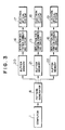
- Fig. 3 illustrates, in block form, another embodiment of a system configuration.
- This system configuration is suitable for electron beam lithography for devices such as custom LSI's which abound in variety but are manufactured on relatively small output basis.
- This embodiment is different from the first embodiment in that the sequence of a series of the pattern data storage buffer memory and pattern generator is reversed.
- pattern data is first divided by a pattern generator 4 into pieces of drawing data, which in turn are stored in buffer memories 20, 21 and 22. It will be appreciated that the buffer memories 20, 21 and 22 are provided in correspondence to respective electron optical systems 17, 18 and 19.
- the individual electron optical systems 17, 18 and 19 can draw different patterns to permit simultaneous lithography for a variety of patterns.
- This embodiment is more costly than the first embodiment by a rise in cost due to the provision of the buffer memory for each electron optical system but the raised cost is not so expensive in total.
- a control circuit system controls a plurality of charged particle optical systems to ensure that the throughput can be improved and at the same time the cost of the lithography system can be reduced.
- the overall lithography system can have a throughput which is n times as large as that of one channel and the cost required for each channel of charged particle optical system associated with the common control circuit system can be approximately halved as compared to the conventional system configuration, in which one control circuit system controls one channel of a charged particle optical system. This permits charged particle beam lithography to be practiced on actual production line in device factories.
Landscapes
- Engineering & Computer Science (AREA)
- Chemical & Material Sciences (AREA)
- Nanotechnology (AREA)
- Physics & Mathematics (AREA)
- Crystallography & Structural Chemistry (AREA)
- Analytical Chemistry (AREA)
- Mathematical Physics (AREA)
- Theoretical Computer Science (AREA)
- Condensed Matter Physics & Semiconductors (AREA)
- General Physics & Mathematics (AREA)
- Manufacturing & Machinery (AREA)
- Electron Beam Exposure (AREA)
Applications Claiming Priority (2)
| Application Number | Priority Date | Filing Date | Title |
|---|---|---|---|
| JP60237498A JPS6298724A (ja) | 1985-10-25 | 1985-10-25 | 電子線描画装置 |
| JP237498/85 | 1985-10-25 |
Publications (3)
| Publication Number | Publication Date |
|---|---|
| EP0220668A2 true EP0220668A2 (fr) | 1987-05-06 |
| EP0220668A3 EP0220668A3 (en) | 1989-01-11 |
| EP0220668B1 EP0220668B1 (fr) | 1992-03-11 |
Family
ID=17016205
Family Applications (1)
| Application Number | Title | Priority Date | Filing Date |
|---|---|---|---|
| EP86114612A Expired EP0220668B1 (fr) | 1985-10-25 | 1986-10-22 | Système de lithographie par faisceau de particules chargées |
Country Status (4)
| Country | Link |
|---|---|
| US (1) | US4829444A (fr) |
| EP (1) | EP0220668B1 (fr) |
| JP (1) | JPS6298724A (fr) |
| DE (1) | DE3684228D1 (fr) |
Cited By (3)
| Publication number | Priority date | Publication date | Assignee | Title |
|---|---|---|---|---|
| EP0736893A3 (fr) * | 1995-04-06 | 1999-07-21 | Fujitsu Limited | Procédé et appareil d'exposition par faisceau de particules chargées |
| US6344655B1 (en) | 1998-07-17 | 2002-02-05 | Advantest Corporation | Multicolumn charged-particle beam lithography system |
| WO2002084719A1 (fr) * | 2001-04-09 | 2002-10-24 | Advantest Corporation | Dispositif et procede d'exposition a un faisceau d'electrons |
Families Citing this family (8)
| Publication number | Priority date | Publication date | Assignee | Title |
|---|---|---|---|---|
| JPS6420619A (en) * | 1987-07-15 | 1989-01-24 | Toshiba Corp | Electron beam aligner |
| US5089774A (en) * | 1989-12-26 | 1992-02-18 | Sharp Kabushiki Kaisha | Apparatus and a method for checking a semiconductor |
| JP3728015B2 (ja) | 1996-06-12 | 2005-12-21 | キヤノン株式会社 | 電子ビーム露光システム及びそれを用いたデバイス製造方法 |
| US6184524B1 (en) | 1996-08-07 | 2001-02-06 | Gatan, Inc. | Automated set up of an energy filtering transmission electron microscope |
| US5798524A (en) * | 1996-08-07 | 1998-08-25 | Gatan, Inc. | Automated adjustment of an energy filtering transmission electron microscope |
| JP2867982B2 (ja) * | 1996-11-29 | 1999-03-10 | 日本電気株式会社 | 半導体装置の製造装置 |
| JPH11329928A (ja) * | 1998-05-12 | 1999-11-30 | Advantest Corp | 電子ビーム露光装置 |
| JP2005276869A (ja) * | 2004-03-23 | 2005-10-06 | Jeol Ltd | 荷電粒子ビーム描画装置。 |
Family Cites Families (6)
| Publication number | Priority date | Publication date | Assignee | Title |
|---|---|---|---|---|
| JPS56124234A (en) * | 1980-03-05 | 1981-09-29 | Hitachi Ltd | Correcting method for electron beam deflection |
| US4430571A (en) * | 1981-04-16 | 1984-02-07 | Control Data Corporation | Method and apparatus for exposing multi-level registered patterns interchangeably between stations of a multi-station electron-beam array lithography (EBAL) system |
| JPS57180128A (en) * | 1981-04-30 | 1982-11-06 | Toshiba Corp | Equipment for electron beam exposure |
| US4390789A (en) * | 1981-05-21 | 1983-06-28 | Control Data Corporation | Electron beam array lithography system employing multiple parallel array optics channels and method of operation |
| US4433384A (en) * | 1981-10-05 | 1984-02-21 | Varian Associates, Inc. | Pattern data handling system for an electron beam exposure system |
| US4694178A (en) * | 1985-06-28 | 1987-09-15 | Control Data Corporation | Multiple channel electron beam optical column lithography system and method of operation |
-
1985
- 1985-10-25 JP JP60237498A patent/JPS6298724A/ja active Pending
-
1986
- 1986-10-22 EP EP86114612A patent/EP0220668B1/fr not_active Expired
- 1986-10-22 DE DE8686114612T patent/DE3684228D1/de not_active Expired - Lifetime
- 1986-10-24 US US06/922,891 patent/US4829444A/en not_active Expired - Lifetime
Cited By (4)
| Publication number | Priority date | Publication date | Assignee | Title |
|---|---|---|---|---|
| EP0736893A3 (fr) * | 1995-04-06 | 1999-07-21 | Fujitsu Limited | Procédé et appareil d'exposition par faisceau de particules chargées |
| US6344655B1 (en) | 1998-07-17 | 2002-02-05 | Advantest Corporation | Multicolumn charged-particle beam lithography system |
| DE19934049C2 (de) * | 1998-07-17 | 2002-06-13 | Advantest Corp | Multikolonnen-Lithographiesystem mit geladenem Teilchenstrahl |
| WO2002084719A1 (fr) * | 2001-04-09 | 2002-10-24 | Advantest Corporation | Dispositif et procede d'exposition a un faisceau d'electrons |
Also Published As
| Publication number | Publication date |
|---|---|
| EP0220668B1 (fr) | 1992-03-11 |
| DE3684228D1 (de) | 1992-04-16 |
| US4829444A (en) | 1989-05-09 |
| JPS6298724A (ja) | 1987-05-08 |
| EP0220668A3 (en) | 1989-01-11 |
Similar Documents
| Publication | Publication Date | Title |
|---|---|---|
| EP0002957B1 (fr) | Appareil d'exposition à faisceau électronique | |
| US4829444A (en) | Charged particle beam lithography system | |
| EP0178156A2 (fr) | Méthode pour le dessin d'un modèle voulu sur une cible par exposition de celle-ci à un faisceau d'électrons | |
| US4853870A (en) | Electron beam exposure system | |
| JPH04273429A (ja) | 荷電粒子ビーム露光の方法と装置 | |
| US6087669A (en) | Charged-particle-beam projection-microlithography apparatus and transfer methods | |
| JPH0691005B2 (ja) | 荷電ビ−ム描画方法 | |
| EP0434990B1 (fr) | Procédé et appareil pour l'exposition par faisceau de particules chargées | |
| JP2669727B2 (ja) | 荷電粒子線露光装置、及び荷電粒子線露光方法 | |
| JPH047087B2 (fr) | ||
| US6541169B1 (en) | Methods for charged-particle-beam microlithography including correction of deflection aberrations, and device-manufacturing methods comprising same | |
| JP2744833B2 (ja) | 荷電粒子ビーム描画方法 | |
| EP0053225B1 (fr) | Système à faisceau électronique et méthode d'utilisation | |
| US20230078311A1 (en) | Multi-charged-particle-beam writing method, multi-charged-particle-beam writing apparatus, and computer-readable recording medium | |
| US6087668A (en) | Charged-particle-beam projection method and apparatus | |
| JPH04309213A (ja) | 荷電ビーム描画方法 | |
| JPH0472613A (ja) | 電子ビームリソグラフイ装置 | |
| JP3340595B2 (ja) | 荷電粒子ビーム描画方法 | |
| US7105844B2 (en) | Method for eliminating low frequency error sources to critical dimension uniformity in shaped beam writing systems | |
| JPH0586850B2 (fr) | ||
| JPS62229830A (ja) | ハイブリツド用荷電粒子ビ−ム描画装置 | |
| JPH0488625A (ja) | 荷電ビーム描画装置 | |
| JPH05234862A (ja) | パターン形成方法 | |
| JPH02183516A (ja) | 電子ビーム露光方法 | |
| JPS62250636A (ja) | 荷電粒子ビ−ム露光装置 |
Legal Events
| Date | Code | Title | Description |
|---|---|---|---|
| PUAI | Public reference made under article 153(3) epc to a published international application that has entered the european phase |
Free format text: ORIGINAL CODE: 0009012 |
|
| 17P | Request for examination filed |
Effective date: 19861022 |
|
| AK | Designated contracting states |
Kind code of ref document: A2 Designated state(s): DE FR GB |
|
| PUAL | Search report despatched |
Free format text: ORIGINAL CODE: 0009013 |
|
| AK | Designated contracting states |
Kind code of ref document: A3 Designated state(s): DE FR GB |
|
| 17Q | First examination report despatched |
Effective date: 19891018 |
|
| GRAA | (expected) grant |
Free format text: ORIGINAL CODE: 0009210 |
|
| AK | Designated contracting states |
Kind code of ref document: B1 Designated state(s): DE FR GB |
|
| REF | Corresponds to: |
Ref document number: 3684228 Country of ref document: DE Date of ref document: 19920416 |
|
| ET | Fr: translation filed | ||
| PLBE | No opposition filed within time limit |
Free format text: ORIGINAL CODE: 0009261 |
|
| STAA | Information on the status of an ep patent application or granted ep patent |
Free format text: STATUS: NO OPPOSITION FILED WITHIN TIME LIMIT |
|
| 26N | No opposition filed | ||
| REG | Reference to a national code |
Ref country code: GB Ref legal event code: IF02 |
|
| PGFP | Annual fee paid to national office [announced via postgrant information from national office to epo] |
Ref country code: FR Payment date: 20050922 Year of fee payment: 20 |
|
| PGFP | Annual fee paid to national office [announced via postgrant information from national office to epo] |
Ref country code: GB Payment date: 20050926 Year of fee payment: 20 |
|
| PGFP | Annual fee paid to national office [announced via postgrant information from national office to epo] |
Ref country code: DE Payment date: 20051202 Year of fee payment: 20 |
|
| PG25 | Lapsed in a contracting state [announced via postgrant information from national office to epo] |
Ref country code: GB Free format text: LAPSE BECAUSE OF EXPIRATION OF PROTECTION Effective date: 20061021 |
|
| REG | Reference to a national code |
Ref country code: GB Ref legal event code: PE20 |