EP0220685A2 - Appareil et méthode pour l'alignement de structures à couches minces formées avec un masque - Google Patents
Appareil et méthode pour l'alignement de structures à couches minces formées avec un masque Download PDFInfo
- Publication number
- EP0220685A2 EP0220685A2 EP86114727A EP86114727A EP0220685A2 EP 0220685 A2 EP0220685 A2 EP 0220685A2 EP 86114727 A EP86114727 A EP 86114727A EP 86114727 A EP86114727 A EP 86114727A EP 0220685 A2 EP0220685 A2 EP 0220685A2
- Authority
- EP
- European Patent Office
- Prior art keywords
- mask
- assembly
- substrate
- holder assembly
- apertured
- Prior art date
- Legal status (The legal status is an assumption and is not a legal conclusion. Google has not performed a legal analysis and makes no representation as to the accuracy of the status listed.)
- Withdrawn
Links
Images

Classifications
-
- C—CHEMISTRY; METALLURGY
- C23—COATING METALLIC MATERIAL; COATING MATERIAL WITH METALLIC MATERIAL; CHEMICAL SURFACE TREATMENT; DIFFUSION TREATMENT OF METALLIC MATERIAL; COATING BY VACUUM EVAPORATION, BY SPUTTERING, BY ION IMPLANTATION OR BY CHEMICAL VAPOUR DEPOSITION, IN GENERAL; INHIBITING CORROSION OF METALLIC MATERIAL OR INCRUSTATION IN GENERAL
- C23C—COATING METALLIC MATERIAL; COATING MATERIAL WITH METALLIC MATERIAL; SURFACE TREATMENT OF METALLIC MATERIAL BY DIFFUSION INTO THE SURFACE, BY CHEMICAL CONVERSION OR SUBSTITUTION; COATING BY VACUUM EVAPORATION, BY SPUTTERING, BY ION IMPLANTATION OR BY CHEMICAL VAPOUR DEPOSITION, IN GENERAL
- C23C14/00—Coating by vacuum evaporation, by sputtering or by ion implantation of the coating forming material
- C23C14/04—Coating on selected surface areas, e.g. using masks
- C23C14/042—Coating on selected surface areas, e.g. using masks using masks
-
- C—CHEMISTRY; METALLURGY
- C23—COATING METALLIC MATERIAL; COATING MATERIAL WITH METALLIC MATERIAL; CHEMICAL SURFACE TREATMENT; DIFFUSION TREATMENT OF METALLIC MATERIAL; COATING BY VACUUM EVAPORATION, BY SPUTTERING, BY ION IMPLANTATION OR BY CHEMICAL VAPOUR DEPOSITION, IN GENERAL; INHIBITING CORROSION OF METALLIC MATERIAL OR INCRUSTATION IN GENERAL
- C23C—COATING METALLIC MATERIAL; COATING MATERIAL WITH METALLIC MATERIAL; SURFACE TREATMENT OF METALLIC MATERIAL BY DIFFUSION INTO THE SURFACE, BY CHEMICAL CONVERSION OR SUBSTITUTION; COATING BY VACUUM EVAPORATION, BY SPUTTERING, BY ION IMPLANTATION OR BY CHEMICAL VAPOUR DEPOSITION, IN GENERAL
- C23C16/00—Chemical coating by decomposition of gaseous compounds, without leaving reaction products of surface material in the coating, i.e. chemical vapour deposition [CVD] processes
- C23C16/04—Coating on selected surface areas, e.g. using masks
- C23C16/042—Coating on selected surface areas, e.g. using masks using masks
-
- H—ELECTRICITY
- H10—SEMICONDUCTOR DEVICES; ELECTRIC SOLID-STATE DEVICES NOT OTHERWISE PROVIDED FOR
- H10P—GENERIC PROCESSES OR APPARATUS FOR THE MANUFACTURE OR TREATMENT OF DEVICES COVERED BY CLASS H10
- H10P72/00—Handling or holding of wafers, substrates or devices during manufacture or treatment thereof
- H10P72/50—Handling or holding of wafers, substrates or devices during manufacture or treatment thereof for positioning, orientation or alignment
- H10P72/57—Mask-wafer alignment
Definitions
- the present invention relates in general to the deposition of depositing thin-film structures, and particularly to an apparatus and a method for thin-film structure patterns on a substrate for a thin-film display device.
- Thin-film display panels (such as LCD or electroluminescent) have been known to be very useful for displaying information as the thin-film structures including the cross electrodes and contact pads, can be deposited on a glass substrate thereby providing a matrix display panel capable of being selectively energized to activate individual pixels thereon.
- One of the problems encountered in the manufacture of thin film display panels is the development of processes that pattern the thin film electrode structures while in an in-line deposition system.
- shadow masking is usually performed over small substrates with stiff masks that are manually clamped to ensure even contact with a particular susbtrate. This is a relatively slow process and usually requires breaking vacuum in the deposition chamber, resulting in some thin-film contamination.
- the substrate is not perfectly flat or not level with respect to its surrounding substrate holder.
- the present invention addresses the problem arising from the difficulties of remote automatic handling of large area shadow masks in an in-line deposition system.
- thin-film patterns have typically been aligned to the substrate and each other by optical means and the substrate is moved manually into position with the aid of a micromanipulator or an optical scanner which provides information to a computer which performs a similar function.
- the aligned substrate is then exposed and wet processed to achieve the desired pattern.
- most shadow masking processes are aligned manually by dropping the masks over pins located on a substrate carrier. Therefore, an apparatus which is effective for remotely operating automatic masking systems where there is a need to eliminate the need for breaking vacuum, which would contaminate deposit of thins films, would be considered an advancement in the art.
- Still another object of the invention is to provide a method of aligning thin-film structures that are to be patterned on the substrate through the use of a vacuum deposition process.
- a further object of the present invention is to provide an apparatus and a method for automatically aligning thin-film structures to be patterned on a substrate while in an in-line deposition system.
- an apparatus for the alignment of thin-film structure patterns on a substrate formed with the use of an apertured mask in a vacuum deposition system comprises a mask frame and a mask assembly affixed to the mask frame, the mask assembly including the apertured mask and mask alignment apertures which are disposed on either side of the mask.
- a mask holder frame is positioned adjacent the mask assembly and is affixed to the mask frame to form a mask holder assembly, the mask holder assembly having primary datum pins affixed thereto and protruding from the side of the holder assembly opposite said mask assembly.
- the alignment apparatus includes a substrate carrier, having a substrate supported therein, positioned adjacent and in operative contact with mask holder assembly; the substrate carrier has primary datum apertures, that engage with the primary pins of the mask holder assembly, which are disposed on the periphery of the carrier.
- the carrier has secondary datum pins protruding therefrom that engage with the mask alignment apertures of the mask assembly.
- a method of aligning thin-film structure patterns on a substrate formed with the use of an apertured mask in a vacuum deposition system comprises the steps of positioning a mask holder assembly within a deposition chamber, such holder assembly having the apertured mask as part thereof and having means for engaging a substrate carrier.
- a substrate carrier is then positioned within the deposition chamber spaced from the mask holder assembly, the carrier having the substrate supported therein and having means for aligning the apertured mask with the substrate.
- the mask holder assembly is then engaged with the substrate carrier such that they are in operative contact.
- a magnet is then positioned in the deposition chamber adjacent the side of the substrate carrier opposite the mask holder assembly such that the apertured mask is held in operative contact with the substrate.
- a thin-film structure material is then vacuum-deposited through the apertured mask and the magnet is then removed from the substrate carrier and the mask holder assembly disengaged from the substrate carrier, thereby resulting in the formation of thin-film structures on the substrate.
- a method of aligning thin-film structure patterns on a substrate formed with the use of an apertured mask in a vacuum deposition system comprises the steps of providing a mask frame and affixing a mask assembly to the mask frame, the mask assembly including the apertured mask and mask alignment apertures that are disposed on either side of the mask.
- a mask holder frame is affixed through the mask assembly to the mask frame to form a mask holder assembly, the mask holder assembly having primary datum pins affixed therethrough and protruding from the side opposite the mask assembly.
- the mask holder assembly is then positioned in a vacuum deposition chamber while a substrate carrier is then positioned in the deposition chamber spaced from the mask holder assembly.
- the carrier has the substrate supported therein and has primary datum apertures disposed about the periphery of the carrier; the carrier has secondary datum pins protruding from the side adjacent the mask holder assembly.
- the mask holder assembly is then engaged with the substrate carrier such that the primary datum pins are first engaged with the primary apertures of the carrier while the secondary datum pins are subsequently engaged with the mask alignment apertures of the mask assembly.
- a magnet is positioned in the deposition chamber adjacent the side of the carrier opposite the mask holder assembly such that the apertured mask is held in operative contact with the substrate; a thin-film structure material is then vacuum-deposited through the apertured mask.
- the magnet is removed from the substrate carrier and the mask holder assembly is disengaged from the substrate carrier thereby resulting in the formation of thin-film structures on the substrate.
- Alignment apparatus 10 is primarily comprised of a mask holder 12 and a substrate carrier 30, which supports (in this case) two substrates.
- mask holder assembly 12 is comprised of a mask frame 14, a mask assembly 20 and a mask holder frame 26.
- mask frame 14 is substantially rectangular in shape and has a frame center support 16, which supports one set of spring forks 18 that aid in engaging mask assembly 20 with substrate carrier 30, and has mask frame pins 17 (see FIG. 1).
- Mask holder frame 26 also has pins 27 located about its periphery (e.g. top and bottom) for allowing mask frame 14 to be affixed thereon.
- Mask assembly 20 has mounting holes 21, for mounting mask assembly 20 to mask frame pins 17, and supports an apertured mask 22 which aids in depositing thin-film structures on a glass substrate.
- Mask assembly 20 also has mask alignment apertures 24 disposed on either side of apertured mask 22.
- mask holder frame 26 has primary datum pins 28 affixed thereto and protruding from the side opposite mask assembly 20. As will be described in detail later in the Specification, primary datum pins 28 serve to engage mask holder assembly 12 with substrate carrier 30.
- substrate carrier 30 is illustrated having at least two substrates 32 supported therein.
- Substrate carrier 30 is also substantially rectangular in shape and has primary apertures 34 disposed about its periphery for engaging the primary datum pins 28 of mask holder assembly 12.
- Primary apertures 34 in this case are two in number and are typically named alignment or registration holes for the purpose of aligning mask holder assembly 12, containing mask assembly 20 with substrates 32 of substrate carrier 30.
- the present invention operates on the basis of a primary and secondary datum reference locations. The primary datum reference locatum is achieved when substrate carrier 30 is positioned adjacent and in operative contact with mask holder assembly 12 such that primary datum apertures 34 will engage with primary datum pins 28.
- Substrate carrier 30 also has a series of secondary datum pins 36 protruding therefrom that are disposed on the carrier side facing mask holder assembly 12. Secondary datum pins 36 will ultimately engage with secondary mask alignment apertures 24 of mask assembly 20. This engagement will nudge apertured mask 22 into the higher accuracy secondary datum reference location (i.e. pins 36 and apertures 24) in order to properly align apertured mask 22 with one of the substrates 32.
- Spring forks 18 of mask frame 14 are considered means for aiding the engagement of mask assembly 20 with secondary datum pins 36 of substrate carrier 30.
- the spring forks are located substantially within and coplanar with mask frame 14.
- a spring fork (i.e. 18) is included for each of the secondary datum (i.e. 36) pins and are in operative contact with mask assembly 20 while being aligned with mask alignment apertures 24.
- apertured mask 22 is structurally relieved from mask assembly 20, which is rigidly attached within mask holder assembly 12, such that the mask is capable of being in operative contact with the substrate of substrate carrier 30.
- Mask alignment apertures 24 of mask assembly 20 include a hole and slot that engage with secondary pins 36 of substrate carrier 30, as illustrated in FIG. 1, and complete the secondary datum reference.
- alignment apparatus 10 further includes a magnet 56 disposed adjacent and in operative contact with substrate carrier 30.
- Magnet 56 is disposed on the side of carrier 30 opposite mask holder frame 26.
- Apertured mask 22, in this particular embodiment, can be designed for patterning electrode structures or electrode pad contacts, but is not limited to such structures.
- the apparatus described in this invention is most effective for remotely operated automatic masking systems where there is a need to eliminate the breaking of vacuum which can contaminate the deposited thin-films.
- the invention provides a final secondary "short-cut" datum registration or alignment system eliminating tolerance build-up caused by chained interregistration of many separate parts by leaping over these registrations and creating a new, independent datum. Without the final secondary "short cut” datum registration afforded by this invention, registration would be through a series of datum mask holder pins, carrier bushings, tooling and glass holders. Even with a 0.001 inch tolerance for each machined part, the total tolerance would be greater than 0.005 inch and unacceptable towards making the patterns register for electrical connection off of a glass display substrate. Furthermore, the method for providing the final registration must be compatible with mechanical shadow masking to prevent blurs and defects in the resulting patterns.
- a typical operation of the alignment apparatus' primary and secondary datum reference system consists of ultimately locating mask assembly 20 over secondary datum pins 36, by first engaging mask holder assembly 12 with the less accurate, chained primary datum of mask frame 14 and substrate carrier 30. As mask holder assembly 12 reaches the end of its primary engagement stroke, mask assembly 20 begins to push mask alignment apertures 24 over the shorter length secondary datum pins 36. This engagement nudges the apertured mask 22 into the higher accuracy secondary datum reference location.
- Spring forks 18, mounted on and about mask frame 14, aid in the engagement of alignment apertures 24 with secondary pins 36. The spring forks press on mask assembly 20 only at the secondary pin locations so that friction does not inhibit lateral movement of mask assembly 20 which would prevent it from aligning with the pin position.
- a hold-down system such as magnet 56 brings mask 22 tight against glass substrate 32.
- Secondary registration or alignment is best performed by using specially shaped apertures 24: a hole on one side of mask 22 and a slot on the other side so that secondary pins 36, utilizing these holes, do not bind with each other. Binding of the secondary datums with the primary datums does not occur because the alignment error between the separate datums is less than the flexible movement of mask 22.
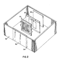
- FIG. 2 there is illustrated alignment apparatus 10 inside a vacuum deposition chamber 50 along with magnet 56 and sputtering apparatus 52.
- FIG. 2 illustrates a portion of a deposition system which may either be from an in-line or from a batch process type system.
- Sputtering apparatus 52 also has a layer of deposition material 54 thereon which will be deposited through apertured mask 22 onto one of the substrates of substrate carrier 30.
- the method comprises the steps of positioning a mask holder assembly 12 within a deposition chamber 50, mask holder assembly 12 having apertured mask 22 as part thereof and having means for engaging substrate carrier 30.
- a substrate carrier 30 is then positioned within deposition chamber 50 spaced from mask holder assembly 12, carrier 30 having a substrate supported therein and having means for aligning apertured mask 22 with the substrate.
- mask holder assembly 12 is engaged with substrate carrier 30 such that they are in operative contact.
- a magnet 56 is then positioned in the deposition chamber adjacent the side of substrate carrier 30 opposite mask holder assembly 12 such that apertured mask 22 is held in operative contact with the substrate.
- Thin-film structure material 54 is then vacuum-deposited through apertured mask 22.
- magnet 56 is removed from substrate carrier 30 and mask holder assembly 12 is disengaged from carrier 30, thereby resulting in the formation of thin-film structures on the substrate.
- mask holder assembly 12 is comprised of mask frame 14, mask assembly affixed to mask frame 14 and a mask holder frame 26 that is affixed through mask assembly 20 to mask frame 14.
- means for engaging substrate carrier 30 includes primary datum pins 28 affixed through and protruding from mask holder assembly 12 on the side opposite mask assembly 20.
- Substrate carrier 30 has primary apertures 34 disposed about the periphery for engaging primary datum pins 28. All of the steps of the method described in aligning the thin-film structure patterns on the substrate can be performed automatically in an in-line deposition system.
- the step of vacuum-depositing includes sputtering, vapor deposition, or chemical vapor deposition.
- This invention can be varied in a number of ways, but the basic operation of prealignment with a primary datum, (i.e. pins 28 and apertures 34) realignment with a more precise secondary datum (i.e. pins 36 and apertures 24), and engagement of the mask assembly with a hold-down spring, remains the same.
- a primary datum i.e. pins 28 and apertures 34
- a more precise secondary datum i.e. pins 36 and apertures 24
- engagement of the mask assembly with a hold-down spring remains the same.
- One can, for example, put bushings on the mask assembly which might engage with pins on the carrier, or one might put bushings on the carrier which engage with pins on the mask assembly, or one might change the shape or location of the hold-down spring which activates the secondary alignment prior to engaging the magnet.
Landscapes
- Chemical & Material Sciences (AREA)
- Chemical Kinetics & Catalysis (AREA)
- Engineering & Computer Science (AREA)
- Materials Engineering (AREA)
- Mechanical Engineering (AREA)
- Metallurgy (AREA)
- Organic Chemistry (AREA)
- General Chemical & Material Sciences (AREA)
- Physical Vapour Deposition (AREA)
- Electroluminescent Light Sources (AREA)
- Devices For Indicating Variable Information By Combining Individual Elements (AREA)
Applications Claiming Priority (2)
| Application Number | Priority Date | Filing Date | Title |
|---|---|---|---|
| US06/790,695 US4746548A (en) | 1985-10-23 | 1985-10-23 | Method for registration of shadow masked thin-film patterns |
| US790695 | 1985-10-23 |
Publications (2)
| Publication Number | Publication Date |
|---|---|
| EP0220685A2 true EP0220685A2 (fr) | 1987-05-06 |
| EP0220685A3 EP0220685A3 (fr) | 1989-03-22 |
Family
ID=25151490
Family Applications (1)
| Application Number | Title | Priority Date | Filing Date |
|---|---|---|---|
| EP86114727A Withdrawn EP0220685A3 (fr) | 1985-10-23 | 1986-10-23 | Appareil et méthode pour l'alignement de structures à couches minces formées avec un masque |
Country Status (5)
| Country | Link |
|---|---|
| US (1) | US4746548A (fr) |
| EP (1) | EP0220685A3 (fr) |
| JP (1) | JPS6299782A (fr) |
| CA (1) | CA1283281C (fr) |
| FI (1) | FI82845C (fr) |
Cited By (4)
| Publication number | Priority date | Publication date | Assignee | Title |
|---|---|---|---|---|
| US4952420A (en) * | 1988-10-12 | 1990-08-28 | Advanced Dielectric Technologies, Inc. | Vapor deposition patterning method |
| EP0525285A1 (fr) * | 1991-07-31 | 1993-02-03 | Minoru Saiki | Porte-échantillon dans un dispositif d'exposition, et dispositif pour l'exposition concurrente de deux surfaces |
| EP0609489A1 (fr) * | 1993-02-02 | 1994-08-10 | Leybold Aktiengesellschaft | Dispositif pour appliquer un masque sur un substrat et/ou pour l'enlever |
| WO2017129245A1 (fr) * | 2016-01-28 | 2017-08-03 | Applied Materials, Inc. | Agencement de masque permettant de masquer un substrat et procédé d'alignement d'un masque sur un substrat |
Families Citing this family (26)
| Publication number | Priority date | Publication date | Assignee | Title |
|---|---|---|---|---|
| DE3925085C1 (fr) * | 1989-07-28 | 1991-01-10 | Battelle-Institut Ev, 6000 Frankfurt, De | |
| US5296916A (en) * | 1991-04-18 | 1994-03-22 | International Business Machines Corp. | Mask alignment system for components with extremely sensitive surfaces |
| JPH05290970A (ja) * | 1992-04-14 | 1993-11-05 | Fuji Electric Co Ltd | 薄膜エレクトロルミネセンス素子の製造方法 |
| US6780465B2 (en) * | 2000-12-28 | 2004-08-24 | Seiko Epson Corporation | Method for making thin film and electronic apparatus |
| US6581278B2 (en) * | 2001-01-16 | 2003-06-24 | St Assembly Test Service Ltd. | Process and support carrier for flexible substrates |
| TW560102B (en) * | 2001-09-12 | 2003-11-01 | Itn Energy Systems Inc | Thin-film electrochemical devices on fibrous or ribbon-like substrates and methd for their manufacture and design |
| US20030068559A1 (en) * | 2001-09-12 | 2003-04-10 | Armstrong Joseph H. | Apparatus and method for the design and manufacture of multifunctional composite materials with power integration |
| US6897164B2 (en) * | 2002-02-14 | 2005-05-24 | 3M Innovative Properties Company | Aperture masks for circuit fabrication |
| US20030151118A1 (en) * | 2002-02-14 | 2003-08-14 | 3M Innovative Properties Company | Aperture masks for circuit fabrication |
| US6821348B2 (en) * | 2002-02-14 | 2004-11-23 | 3M Innovative Properties Company | In-line deposition processes for circuit fabrication |
| US7006202B2 (en) * | 2002-02-21 | 2006-02-28 | Lg.Philips Lcd Co., Ltd. | Mask holder for irradiating UV-rays |
| KR100480705B1 (ko) * | 2002-07-03 | 2005-04-06 | 엘지전자 주식회사 | 유기 el 소자 제작용 새도우 마스크 및 그 제조 방법 |
| US7410919B2 (en) * | 2003-06-27 | 2008-08-12 | International Business Machines Corporation | Mask and substrate alignment for solder bump process |
| US20060086321A1 (en) * | 2004-10-22 | 2006-04-27 | Advantech Global, Ltd | Substrate-to-mask alignment and securing system with temperature control for use in an automated shadow mask vacuum deposition process |
| JP4331707B2 (ja) * | 2004-12-16 | 2009-09-16 | 三星モバイルディスプレイ株式會社 | 整列システム、垂直型トレイ移送装置及びこれを具備した蒸着装置 |
| US20070137568A1 (en) * | 2005-12-16 | 2007-06-21 | Schreiber Brian E | Reciprocating aperture mask system and method |
| US7763114B2 (en) * | 2005-12-28 | 2010-07-27 | 3M Innovative Properties Company | Rotatable aperture mask assembly and deposition system |
| US20070262326A1 (en) * | 2006-05-10 | 2007-11-15 | Touchtek Corporation | LED multi-layer metals primary electrodes manufacturing process & installation |
| US7690104B2 (en) * | 2008-02-20 | 2010-04-06 | Apple Inc. | Technique for reducing wasted material on a printed circuit board panel |
| US20110107964A1 (en) * | 2009-11-10 | 2011-05-12 | Molten Corporation | Object Holding Apparatus |
| US20130092085A1 (en) * | 2011-10-17 | 2013-04-18 | Synos Technology, Inc. | Linear atomic layer deposition apparatus |
| US9051637B2 (en) * | 2011-11-10 | 2015-06-09 | Veeco Ald Inc. | Securing of shadow mask and substrate on susceptor of deposition apparatus |
| US9579680B2 (en) * | 2013-01-31 | 2017-02-28 | Wki Holding Company, Inc. | Self-centering magnetic masking system |
| US20140240859A1 (en) * | 2013-02-28 | 2014-08-28 | Corning Incorporated | Optic obscuration assembly, method and system for working on an optical element, and resulting optical element |
| CN103882375B (zh) * | 2014-03-12 | 2016-03-09 | 京东方科技集团股份有限公司 | 一种掩膜板及其制作方法 |
| US11715662B2 (en) * | 2020-12-11 | 2023-08-01 | Applied Materials, Inc. | Actively clamped carrier assembly for processing tools |
Family Cites Families (13)
| Publication number | Priority date | Publication date | Assignee | Title |
|---|---|---|---|---|
| US3510349A (en) * | 1966-11-15 | 1970-05-05 | Us Air Force | Vacuum deposited interconnection matrix |
| US3678892A (en) * | 1970-05-19 | 1972-07-25 | Western Electric Co | Pallet and mask for substrates |
| US4013502A (en) * | 1973-06-18 | 1977-03-22 | Texas Instruments Incorporated | Stencil process for high resolution pattern replication |
| US4096821A (en) * | 1976-12-13 | 1978-06-27 | Westinghouse Electric Corp. | System for fabricating thin-film electronic components |
| JPS54103552A (en) * | 1978-02-01 | 1979-08-15 | Hitachi Electronics | Pattern formation method |
| US4344988A (en) * | 1978-08-01 | 1982-08-17 | Nippon Sheet Glass Co., Ltd. | Method for forming patterned coating |
| US4303489A (en) * | 1978-08-21 | 1981-12-01 | Vac-Tec Systems, Inc. | Method and apparatus for producing a variable intensity pattern of sputtering material on a substrate |
| US4278710A (en) * | 1979-08-27 | 1981-07-14 | The United States Of America As Represented By The Secretary Of The Navy | Apparatus and method for submicron pattern generation |
| US4305801A (en) * | 1980-04-16 | 1981-12-15 | The United States Of America As Represented By The United States Department Of Energy | Line-of-sight deposition method |
| US4335161A (en) * | 1980-11-03 | 1982-06-15 | Xerox Corporation | Thin film transistors, thin film transistor arrays, and a process for preparing the same |
| US4492180A (en) * | 1981-03-16 | 1985-01-08 | Applied Magnetics Corporation | Apparatus for indexing and registering a selected deposition mask to a substrate and method therefor |
| US4511599A (en) * | 1983-03-01 | 1985-04-16 | Sigmatron Associates | Mask for vacuum depositing back metal electrodes on EL panel |
| US4615781A (en) * | 1985-10-23 | 1986-10-07 | Gte Products Corporation | Mask assembly having mask stress relieving feature |
-
1985
- 1985-10-23 US US06/790,695 patent/US4746548A/en not_active Expired - Lifetime
-
1986
- 1986-10-07 CA CA000519971A patent/CA1283281C/fr not_active Expired - Lifetime
- 1986-10-22 JP JP61249799A patent/JPS6299782A/ja active Pending
- 1986-10-23 FI FI864307A patent/FI82845C/fi not_active IP Right Cessation
- 1986-10-23 EP EP86114727A patent/EP0220685A3/fr not_active Withdrawn
Cited By (7)
| Publication number | Priority date | Publication date | Assignee | Title |
|---|---|---|---|---|
| US4952420A (en) * | 1988-10-12 | 1990-08-28 | Advanced Dielectric Technologies, Inc. | Vapor deposition patterning method |
| WO1990004320A3 (fr) * | 1988-10-12 | 1990-09-07 | Advanced Dielectric Tech | Procede de formation de motifs par depot en phase de vapeur et produits ainsi obtenus |
| EP0525285A1 (fr) * | 1991-07-31 | 1993-02-03 | Minoru Saiki | Porte-échantillon dans un dispositif d'exposition, et dispositif pour l'exposition concurrente de deux surfaces |
| EP0609489A1 (fr) * | 1993-02-02 | 1994-08-10 | Leybold Aktiengesellschaft | Dispositif pour appliquer un masque sur un substrat et/ou pour l'enlever |
| US5503675A (en) * | 1993-02-02 | 1996-04-02 | Leybold Aktiengesellschaft | Apparatus for applying a mask to and/or removing it from a substrate |
| WO2017129245A1 (fr) * | 2016-01-28 | 2017-08-03 | Applied Materials, Inc. | Agencement de masque permettant de masquer un substrat et procédé d'alignement d'un masque sur un substrat |
| CN108603279A (zh) * | 2016-01-28 | 2018-09-28 | 应用材料公司 | 用于掩蔽基板的掩模布置和用于将掩模与基板对准的方法 |
Also Published As
| Publication number | Publication date |
|---|---|
| CA1283281C (fr) | 1991-04-23 |
| JPS6299782A (ja) | 1987-05-09 |
| FI82845B (fi) | 1991-01-15 |
| FI864307A0 (fi) | 1986-10-23 |
| EP0220685A3 (fr) | 1989-03-22 |
| FI82845C (fi) | 1991-04-25 |
| FI864307A7 (fi) | 1987-04-24 |
| US4746548A (en) | 1988-05-24 |
Similar Documents
| Publication | Publication Date | Title |
|---|---|---|
| US4915057A (en) | Apparatus and method for registration of shadow masked thin-film patterns | |
| US4746548A (en) | Method for registration of shadow masked thin-film patterns | |
| US4615781A (en) | Mask assembly having mask stress relieving feature | |
| JP4216531B2 (ja) | アラインメントデバイス及び有機材料の蒸着方法 | |
| KR100811730B1 (ko) | 마스크막형성방법 및 마스크막형성장치 | |
| US20030108805A1 (en) | Aligning mask segments to provide an assembled mask for producing oled devices | |
| JPH10152776A (ja) | 基板支持具および基板の支持方法 | |
| US4715940A (en) | Mask for patterning electrode structures in thin film EL devices | |
| US20090026678A1 (en) | Alignment precision enhancement of electronic component process on flexible substrate device and method thereof the same | |
| EP0104242B1 (fr) | Procede et appareil pour maintenir un substrat dans un support | |
| US4563085A (en) | Method of producing lithographic plates | |
| US4529303A (en) | Apparatus for producing lithographic plates | |
| EP0103671B1 (fr) | Procédé et appareil pour fabriquer une configuration métallique sur un substrat céramique | |
| KR102406220B1 (ko) | Ldi 방식을 이용한 oled 증착용 메탈 마스크 제조 방법 | |
| US11626272B2 (en) | Sputtering equipment and operation method thereof | |
| JP2933790B2 (ja) | 液晶表示素子の製造方法 | |
| JP3415177B2 (ja) | スパッタ用治具 | |
| JP4017321B2 (ja) | 組立装置 | |
| JP2000321544A (ja) | 液晶表示素子製造装置 | |
| JPH0822131A (ja) | 露光における位置合わせ装置 | |
| KR101696713B1 (ko) | 기판 정렬 장치 | |
| KR200147995Y1 (ko) | 평판소자의 인쇄테이블 | |
| JPH1068921A (ja) | 液晶表示素子の製造方法および液晶表示素子製造装置 | |
| KR20050022749A (ko) | 기판과 마스크를 밀착시키는 방법과 장치 그리고 이를이용한 스퍼터링 방법 및 장치 | |
| CN116695066A (zh) | 一种掩膜板、蒸镀方法以及蒸镀设备 |
Legal Events
| Date | Code | Title | Description |
|---|---|---|---|
| PUAI | Public reference made under article 153(3) epc to a published international application that has entered the european phase |
Free format text: ORIGINAL CODE: 0009012 |
|
| 17P | Request for examination filed |
Effective date: 19861023 |
|
| AK | Designated contracting states |
Kind code of ref document: A2 Designated state(s): BE DE FR GB NL |
|
| PUAL | Search report despatched |
Free format text: ORIGINAL CODE: 0009013 |
|
| AK | Designated contracting states |
Kind code of ref document: A3 Designated state(s): BE DE FR GB NL |
|
| 17Q | First examination report despatched |
Effective date: 19900921 |
|
| STAA | Information on the status of an ep patent application or granted ep patent |
Free format text: STATUS: THE APPLICATION IS DEEMED TO BE WITHDRAWN |
|
| 18D | Application deemed to be withdrawn |
Effective date: 19920501 |
|
| RIN1 | Information on inventor provided before grant (corrected) |
Inventor name: BOUDREAU, ROBERT A. Inventor name: WILKIE, ROBERT J. |