EP0220732A2 - Verfahren und Vorrichtung zur Ablesung eines Bandmusters - Google Patents
Verfahren und Vorrichtung zur Ablesung eines Bandmusters Download PDFInfo
- Publication number
- EP0220732A2 EP0220732A2 EP86115046A EP86115046A EP0220732A2 EP 0220732 A2 EP0220732 A2 EP 0220732A2 EP 86115046 A EP86115046 A EP 86115046A EP 86115046 A EP86115046 A EP 86115046A EP 0220732 A2 EP0220732 A2 EP 0220732A2
- Authority
- EP
- European Patent Office
- Prior art keywords
- band
- positions
- density data
- lane
- lanes
- Prior art date
- Legal status (The legal status is an assumption and is not a legal conclusion. Google has not performed a legal analysis and makes no representation as to the accuracy of the status listed.)
- Granted
Links
Images


Classifications
-
- G—PHYSICS
- G01—MEASURING; TESTING
- G01T—MEASUREMENT OF NUCLEAR OR X-RADIATION
- G01T1/00—Measuring X-radiation, gamma radiation, corpuscular radiation, or cosmic radiation
- G01T1/29—Measurement performed on radiation beams, e.g. position or section of the beam; Measurement of spatial distribution of radiation
- G01T1/2914—Measurement of spatial distribution of radiation
- G01T1/2921—Static instruments for imaging the distribution of radioactivity in one or two dimensions; Radio-isotope cameras
- G01T1/2942—Static instruments for imaging the distribution of radioactivity in one or two dimensions; Radio-isotope cameras using autoradiographic methods
-
- G—PHYSICS
- G01—MEASURING; TESTING
- G01N—INVESTIGATING OR ANALYSING MATERIALS BY DETERMINING THEIR CHEMICAL OR PHYSICAL PROPERTIES
- G01N27/00—Investigating or analysing materials by the use of electric, electrochemical, or magnetic means
- G01N27/26—Investigating or analysing materials by the use of electric, electrochemical, or magnetic means by investigating electrochemical variables; by using electrolysis or electrophoresis
- G01N27/416—Systems
- G01N27/447—Systems using electrophoresis
- G01N27/44704—Details; Accessories
- G01N27/44717—Arrangements for investigating the separated zones, e.g. localising zones
- G01N27/44721—Arrangements for investigating the separated zones, e.g. localising zones by optical means
Definitions
- the present invention relates to a method of and apparatus for automatically reading a band arrayal pattern, and more particularly to a band arrayal pattern-automatic reading method and apparatus which are well suited to read the base band arrayal pattern of a gene imaged on an X-ray film and to correctly detect the band arrayal order of base codes.
- the gene of a living organism is composed of the substance deoxyribonucleic acid (DNA) and has a structure in which the four kinds of organic bases; adenine (A), cytosine (C), guanine (G) and thymine (T) are arrayed in a double-helical shape.
- a method of determining the base arrayal of the DNA is the shotgun method. With this method, the chain of the DNA is broken up by reagents for chemically cutting the respective bases, and the individual bases are arrayed in accordance with their different lengths by electrophoresis, whereupon they are imaged on a film with X-rays.
- the X-ray film obtained after the electrophoresis bears belt-like patterns expressive of the arrayal of the four kinds of bases.
- a plurality of bands 4 extending substantially perpendicularly to a lane are arrayed within the lane which is the valid range of each of the base codes A, C, G and T.
- the gene can be analyzed by analyzing the base arrayal on this film.
- the base arrayal pattern on the film is input to a computer.
- a digitizer in which the X-ray film 3 is placed on the digitizer, and the positions of the bands 4 on the film 3 are successively pointed to with a pen or cursor so as to input the output signals of the digitizer to the computer.
- An object of the present invention is to provide a method of and apparatus for automatically reading band positions more easily.
- a pattern having a plurality of bands in each of a plurality of lanes is photoelectrically converted, the sum (histogram) of the density data (pixel data) of pixels lying on lines each of which passes through a plurality of points in a direction perpendicular to the lanes is detected on the basis of the density data of the respective pixels photoelectrically converted, points representative of the existence regions of the respective lanes, for example, the central positions of the respective lanes are detected from the histogram, the density data items of the pixels on the detected central positions of the respective lanes are collected to obtain the spectra of the respective lanes, and the spectra are used to detect the plurality of maximum positions of each of them as band positions.
- lane positions are accurately found, so that band representative positions, for example, central positions can be accurately found.
- the histogram in the direction perpendicular to the lanes is obtained every minute section in the extending direction of the lanes, and the positions of the representative points of the lane regions, for example, the central positions of the lanes are found for each of such sections.
- the band positions can be accurately found.
- the positions of the central points of the lanes and the points of both the ends of the lanes are found as points representative of the lane regions, spectra in the extending direction of the lanes are obtained for the respective positions found, and the spectra are analyzed, thereby to find the central position and both end positions of respective bands.
- the band positions can be correctly detected.
- an apparatus well-suited to perform the method of the present invention comprises a first memory which has storage locations corresponding to different positions in a direction perpendicular to lanes, a second memory in which pixel data items obtained by photoelectric conversion are stored in correspondence with the two-dimensional positions of the respective pixels of a pattern, means to add each pixel data on a single line of the pattern perpendicular to the lanes and the data of the corresponding position perpendicular to the lanes already written in said first memory and write a result into said first memory again in synchronism with the photoelectric conversion of the pixel on the single line, so as to form histogram data for the respective positions perpendicular to the lanes, and means to detect a position of a point representative of an existence region of each lane on the basis of the histogram of said first memory, to read out of said second memory the pixel data items corresponding to the pixels on a line passing the detected point so as to obtain spectral data for each lane, and to detect a maximum position
- the band positions in the plurality of lanes on the pattern can be detected at high speed.
- the addition means obtains the histogram every predetermined section in the extending direction of the lanes.
- the second memory consists of two areas for storing the pixel data items within two such sections, and in obtaining the histogram for a new section, the two areas are successively exchanged and used.
- the second memory need not store all the pixel data items on the pattern but may store the pixel data items every fixed section, so that the apparatus is simplified.
- the positions of bands arrayed forming lanes adjacent to each other are detected for the respective lanes, each of the detected band positions is normalized to a position on a single line in the lengthwise direction of the lane in accordance with the slope of the individual band, and the arrayal order of the bands is thereafter read.
- the arrayal order of the bands can be correctly detected.
- the positions of bands arrayed forming lanes adjacent to each other are detected for the respective lanes, and each of the detected band positions is normalized to a position on a single line in the lengthwise direction of the lane in accordance with the slope of the individual band.
- the band interval of bands adjoining each other on the single line is compared with the smallest band interval as predetermined and a reference band interval depending upon a position on the single line, and the band is erased or re-detected.
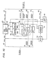
- Fig. 1A is a block system diagram of an embodiment of a band arrayal pattern-reading apparatus according to the present invention
- Fig. 1B is a view showing the schematic arrangement of an image scanner 5
- Fig. 1C is a diagram showing the internal arrangement of an interface circuit 8.
- Numeral 3 designates an X-ray film, on which bands 4 in solid lines corresponding to the four kinds of base codes A, C, G and T with their arrayal determined by the shotgun method are arrayed and imaged.
- This X-ray film 3 is positioned so that the lengthwise direction of lanes being the valid ranges of the respective bases A, C, G and T may come into substantial agreement with the direction of the Y-axis of the image scanner 5.
- Numeral 2 designates a plate of transparent glass, which is set in the image scanner 5 and on which the X-ray film 3 is placed.
- the size of the transparent glass 2 is, for example, A3-size or so.
- a unidimensional image sensor 6 is disposed in correspondence with the position of the transparent glass 2.
- a unidimensional light emitting device 7 projects light on the X-ray film 3. Then, reflected light corresponding to one line in the direction of the X-axis of the X-ray film 3 enters the image sensor 6.
- the image sensor 6 photoelectrically converts the reflected light for one line in pixel unit, and thereafter derives electric signals serially by the use of a charge coupled device (CCD) or the like (not shown) built therein. It A/D-converts the derived electric signals into digital signals of, for example, 8 bits and delivers these signals.
- CCD charge coupled device
- the image sensor 6 and the light emitting device 7 are moved at equal speeds in the Y-axial direction by a driving mechanism (not shown) so as to read the X-ray film 3 and detect the bands.
- the image scanner 5 is constructed as shown in Fig. 1B. It reads the X-ray film 3, and delivers pixel data being the read result.
- Shown at numeral 9 are operation keys, which include a start key etc.
- the depression of this start key starts the reading processing of the X-ray film 3.
- the interface circuit 8 has an image memory, an addition memory etc. built therein. It is connected to the image scanner 5 as well as the operation keys 9, and it forms the interface between the image scanner 5 and a CPU 12 through a bus line 13.
- the CPU 12 serves to execute the reading of the band arrayal and the corrections of the positions of the read bands.
- Numeral 14 indicates a ROM in which a program for load is stored.
- Numeral 16 indicates a disk device, in which a band arrayal reading program is stored and also base code data having been read is stored.
- the loading program stored in the ROM 14 is run, and the band arrayal reading program stored in the disk device 16 is loaded in a RAM 15.
- the RAM 15 has an area SD for storing base data, an area for a band interval function, etc.
- Numeral 17 denotes an external interface, which serves to transmit the read base code data to an external computer (not shown).
- the interface circuit 8, CPU 12, ROM 14, RAM 15, disk device 16 and interface portion 17 are interconnected through the bus line 13.
- the image scanner 5 supplies the interface circuit 8 with the pixel data after it has photoelectrically converted the image of the X-ray film 3 on the transparent glass 2 in pixel unit.
- the loading program stored in the ROM 14 is run, and the band arrayal reading program stored in the disk device 16 is loaded in the RAM 15.
- the CPU 12 executes the band arrayal reading program loaded in the RAM 15 and delivers various control signals to the interface circuit 8 through the bus line 13.
- the pixel data applied to the interface circuit 8 is processed on the basis of the control signals.
- the base data being the processed result is output to, for example, the external computer (not shown) through the external interface 17.
- Numeral 30 designates a control circuit, which supplies operation control signals to an address counter 38, a status register 36, a command register 33, an addition memory 47 and a latch circuit 45 in accordance with an address signal and a control signal respectively applied from the CPU 12 to terminals 31 and 32 through the bus line 13.
- the command register 33 is connected to the control circuit 30. It stores control signals for the image scanner and the driving mechanism (not shown) thereof applied to a terminal 34, and supplies the control signals to the image scanner 5 and the driving mechanism through a terminal 35 in accordance with the operation signals received from the control circuit 30.
- the status register 36 is connected to the address counter 38 and the control circuit 30. It stores the status signals of the image scanner 5 and the driving mechanism thereof applied to a terminal 37 and the status signals of the control circuit 30 and the address counter 38 inside the interface circuit 8, and supplies the status signals from a terminal 39 to the CPU 12 through the bus line 13 under the control of the control circuit 30.
- the address counter 38 is connected to an image memory 40, the control circuit 30, the status register 36 and the addition memory 47. It is constructed of an X-counter 38a which counts clock pulses supplied from the control circuit 30 and generates an address corresponding to a pixel position on one line in the X-axial direction, and a Y-counter 38b which counts the carry pulses of the X-counter and generates an address corresponding to a pixel position in the Y-axial direction.
- the output addresses of the X-counter 38a and Y-counter 38b are supplied to the image memory 40, and the output address of the X-counter 38a is further supplied to the addition memory 47.
- the image memory 40 consists of a first area 41 and a second area 42, and is connected to the address counter 38 and the control circuit 30. It stores pixel data applied from a terminal 42, in accordance with the X and Y addresses set by the address counter 38, and it reads out the stored pixel data and supplies the read data to the CPU 12 through a terminal 43 in accordance with the operation control signal received from the control circuit 30.
- Shown at numeral 44 is an adder, which is connected to the addition memory 47 and the latch circuit 45. It adds the pixel data received from the terminal 42 and addition pixel data latched in the latch circuit 45, and delivers the result to the addition memory 47.
- the addition memory 47 is connected to the adder 44, the address counter 38, the control circuit 30 and the latch circuit 45.
- the addition pixel data delivered from the adder 44 is stored in the addition memory 47 in correspondence with the X address supplied from the address counter 38, and it is read out to be delivered to the latch circuit 45 and also supplied to the CPU 12 through a terminal 46 in accordance with the operation control signal received from the control circuit 30.
- the latch circuit 45 is connected to the control circuit 30, the adder 44 and the addition memory 47. It latches the addition pixel data read out from the addition memory 47, and delivers the latched addition pixel data to the adder 44 in accordance with the latch pulse received from the control circuit 30.
- a spectrum obtained at the step 100 is analyzed to detect band positions.
- the band positions detected at the step 200 are normalized.
- base code data is corrected. That is, base data is checked, base data detected erroneously is erased, and base data having failed to be detected is compensated for.
- the base data items are read out in the order of addresses corresponding to the Y-axial direction, to be stored in the disk device 16 and to be transmitted from the external interface 17 to the external computer (not shown).
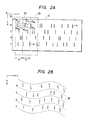
- Fig. 2A shows the X-ray film 3, on which the plurality of bands 4 are arrayed in correspondence with each of the bases A, C, G and T.
- Fig. 2B similarly shows the X-ray film 3.
- the respective lanes are not rectilinear but are meandering.
- the X-ray film 3 having the meandering lanes in this manner, when the spectral data items are collected assuming the lanes in the whole X-ray film to be rectilinear, it becomes impossible to discriminate the lane of the base to which the spectrum collected near the boundary of the adjacent lanes indicated by a broken line in Fig. 2B belongs.
- the X-ray film 3 is divided every fixed section d1 in the Y-axial direction as indicated by dotted lines in Fig. 2A, a histogram is prepared for each divided section d1, the histogram is analyzed to detect the X-axial positions of the respective lanes of the base codes A, C, G and T, and the lanes are thereafter sampled.
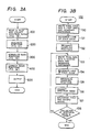
- Fig. 3B is a flow chart of the processing which is executed at the step 100. The processing of the film reading and the spectrum collection to be executed by this flow chart will be described with reference to Fig. 1C.
- the CPU 12 supplies a control signal to the image sensor 6 through the interface circuit 8, whereby the image sensor 6 is moved at a fixed speed by the distance d1 (for example, several tens mm) in the Y-axial direction by means of the driving mechanism (not shown).
- the distance d1 for example, several tens mm
- the driving mechanism not shown.
- d2 1/16 mm
- the image sensor 6 serially delivers pixel data (detection data) corresponding to one line in the X-axial direction.
- the pixel data items are supplied to the interface circuit 8, and are successively written into the image memory 40 built in the interface circuit 8.
- the pixel data is added by the adder 44 in the interface circuit 8 with addition pixel data read out from the address of the addition memory 47 corresponding to each detection position of one line in the X-axial direction, and the result is stored in the same read-out address of the addition memory 47.
- the addition data items each being the sum of the pixel data for the minute distance d2 in the Y-axial direction are stored in parallel into the addresses of the addition memory 47 corresponding to the respective detection positions of one line in the X-axial direction, and a histogram is obtained.
- Pixel data items D1, D2 and D3 serially transmitted as shown in Fig. 4A are input to the terminal 42 shown in Fig. 1C, and are supplied to the image memory 40 and the adder 44.
- the X counter 38a of the address counter 38 changes its output address value as shown in Fig. 4B.
- the control circuit 30 supplies the addition memory 47 with an operation control signal (write strobe) as shown in Fig. 4C, and the addition memory 47 writes data in the low level interval of the write strobe and reads data in the high level interval thereof.
- the image memory 40 is also supplied with the same write strobe as shown in Fig. 4C, and data is written into the image memory 40 in the low level interval of the write strobe.
- the addition memory 47 has addresses corresponding to the respective detection positions of one line in the X-axial direction, and the contents of all the addresses are cleared to zero when the CPU 12 commands the image sensor 6 to start reading. Thereafter, the addition memory 47 reads out addition pixel data stored in the address designated by the X counter 38a, in the high level interval of the write strobe shown in Fig. 4C.
- the latch circuit 45 is supplied from the control circuit 30 with latch pulses which are obtained by inverting the write strobe as shown in Fig. 4D. It latches the addition pixel data at the point of time of the rise of the latch pulse, namely, at the point of time of the end of the reading of the addition memory 47. Thus, the addition pixel data is supplied from the latch circuit 45 to the adder 44.
- the addition pixel data changes as shown in Fig. 4E. Accordingly, the addition pixel data which is the addition value between the pixel data applied from the terminal 42 to the adder 44 and the addition pixel data from the latch circuit 45 changes as shown in Fig. 4F.
- addition pixel data items hatched are written into the addition memory 47 in the low level intervals of the strobe shown in Fig. 4C.
- this addition pixel data S2 is latched in the latch circuit 45 at the point of time of the end of the high level interval of the write strobe in Fig. 4C, whereupon the read pixel data D2 and the output S2 of the latch circuit are added and are written into the image memory 47 as addition pixel data (S2 + D2).
- the addition pixel data or the histograms which are the summations of the pixel data provided every minute distance d1 in the Y-axial direction are stored in the addresses of the addition memory 47 corresponding to the respective pixel positions (detection positions) in the X-axial direction.
- the image memory 40 is divided into the first area 41 and the second area 42 in accordance with the most significant bit of the output address of the Y counter 38b.
- the CPU 12 first commands the image sensor 6 to read the data, the value of the most significant bit is "0" and the first area 41 is selected. Thereafter, each time the reading is commanded, the value of the most significant bit changes. That is, the area 41 is selected for the most significant bit of "0,” and the area 42 for the most significant bit of "1.”
- the address of the address counter 38 to be supplied to the image memory 40 is incremented each time the pixel data is input from the terminal 42.
- the pixel data items obtained while the image sensor 6 is first moved by the distance d1 as described above are all stored in the first area 41.
- the pixel data items obtained while the image sensor 6 is subsequently moved by the distance d1 are all stored in the second area 42.
- the pixel data items from the X-ray film 3 are read and written into the image memory 40, the pixel data items of the predetermined section (of the distance d1) in the Y-axial direction are added for the respective pixel positions in the X-axial direction, and the results are written into the addition memory 47 to generate the histograms.
- the pixel data items of the predetermined section (of the distance d1) in the Y-axial direction are added for the respective pixel positions in the X-axial direction, and the results are written into the addition memory 47 to generate the histograms.
- the above is the contents of the step 130.
- histograms need to be obtained in such a way that the values of pixel data in the predetermined section d1 in the Y-axial direction of the lanes are added for pixel positions in the X-axial direction of the lanes of the respective bases A, C, G and T.
- the read pixel data items are added for the respective pixel positions in the X-axial direction by means of the adder 44, whereby addition pixel data or the histograms for the respective pixel positions in the X-axial direction are obtained simultaneously and in parallel with the reading of the pixel data.
- the generation of the histograms is performed fast by the hardware of the adder 44 etc., and can therefore be processed simultaneously and in parallel with the writing of the pixel data into the image memory 40.
- the generation of the histograms is performed by the addition memory 47 as well as the single adder 44, and the latch circuit 45 attendant thereon, so that the number of components is small and that the circuit arrangement is simple.
- the addition data items which are the sums of the pixel data obtained every minute distance d2 in the Y-axial direction are stored in the addresses of the addition memory 47 corresponding to the respective detection positions of one line in the X-axial direction, and the histograms are generated.
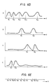
- a waveform as shown in Fig. 5A is obtained.
- the CPU 12 differentiates the histograms of the addition memory 47 with respect to the X direction, to obtain differential values the analog conversion values of which become a waveform as shown in Fig. 5B, and it stores the differential values in a working area (not shown) within the RAM 15. Further, with reference to the plus maximum value and minus maximum value of the differential values, a plus threshold value THH and a minus threshold value THL which are respectively equal to 1/2 of the plus and minus maximum values by way of example are set.
- x LA , x RA , x LC , x RC , x LG , x RG , x LT and x RT are found and are recognized as the positions of the X-axial left and right ends of the lanes of the respective base codes A, C, G and T in the partial region 31 (Fig. 2A) (step 131).
- the values of the middle points x MA , x MC , x MG , and x MT of the respective points x LA and x RA , x LC and x RC , x LG and x RG , and x LT and x RT are calculated.
- the boundary values of the lane may be set by proportionally assigning the interspace between found lanes corresponding to other bases.
- a section where they are not found may be divided in two, the middles of the divided parts being set as the centers of the lanes.
- the CPU 12 collects the spectral data between the points p LA and p′ LA in such a way that the pixel data items of positions (addresses) corresponding to the line connecting the points p Li and p′ Li are read out successively in a direction from the point p Li to the point p′ Li and are successively written into predetermined addresses within the RAM 15. Likewise, the spectral data items between the points p MA and p′ MA and between the points p RA and p′ RA are collected.
- each of the base codes A, C, G and T has the spectral data collected at the three points of both the ends and the middle of the band.
- the first area 41 and second area 42 of the image memory 40 are exchanged and used (step 137).
- the processing control proceeds to the step 133.
- the first area 41 and second area 42 of the image memory 40 have been exchanged at the step 137.
- the pixel data items of the region 33 (Fig. 2A) of the next distance d1 are successively written into the area (for example, the first area 41) opposite to the area (for example, the second area 42) within the image memory 40 in which the pixel data items were written at the preceding time.
- the steps 133 - 137 are repeatedly executed thereby to collect the spectral data of the whole area of the X-ray film 3. Then, the step 100 ends.
- Fig. 3C shows the detailed flow chart of the processing 200.
- the CPU 12 reads out the respective spectra S(y) from the RAM 15 and differentiates them to obtain differential spectra S′(y) the analog conversion values of which become a waveform shown in Fig. 6B.
- a plus threshold value THH and a minus threshold value THL which are respectively equal to 1/2 of the plus maximum value and minus maximum value by way of example are set (step 231).
- Y-axial values y1, y4, y7 ?? at which the differential spectra S′(y) change from a value not less than the plus threshold value THH to a value less than the same and Y-axial values y3, y6, y9 « at which the differential spectra S′(y) change from a value not less than the minus threshold value THL to a value less than the same are found to detect the existence ranges of peaks y1 - y3, y4 - y6, y7 - y9, « (step 232).
- Parts indicated by dotted lines in Figs. 6A and 6B are the existence ranges of peaks.
- a Y-axial value y2 at which the differential spectrum S′(y) is zero and accordingly the spectrum S(y) becomes the maximum is found.
- Y-axial values y5, Y8, « at which the differential spectrum S′(y) is zero and accordingly the spectrum S(y) becomes the maximum are found in the respective existence ranges of peaks y4 - y6, y7 - y9, « (step 233).
- the values y3, y5, y8, « obtained here are the positions of the peak points.
- the reason why the peak existence range is first detected in this manner is as follows:
- the spectrum S(y) might contain noise N attributed to dust etc. Therefore, an erroneous band position will be detected merely by finding only the value at which the differential spectrum S′(y) is zero.
- the plus threshold value THH and minus threshold value THL are set, and the peak existence range is obtained, whereupon the value at which the differential spectrum S′(y) is zero is found within the peak existence range. Therefore, the noise N is not detected as the band position.
- Fig. 6D shows the analytical spectra SS(y) expressive of the band positions as obtained for the respective bases A, G, T and C.
- the analytical spectra SS(y) are stored in the RAM 15 as a table wherein addresses are assigned to the respective pixels in the Y-axial direction and wherein the value of the existence position of the band is "1" and that of the non-existence position thereof is "0" by way of example
- the position of the spectrum corresponding to the band has a certain width in the Y-axial direction as shown by S(y) in Fig. 6A.
- the width differs for the individual bands, and also the density values of the individual bands differ. Therefore, the band existence range is detected using the differential spectrum S′(y), and the point at which the differential spectrum S′(y) is zero and accordingly the spectrum S(y) becomes the maximum is detected as the band position from within the band existence range, whereby the existence position of the band can be accurately specified irrespective of the density of the band and the magnitude of the band width.
- the plus threshold value THH is compared with a predetermined value ⁇ (step 234).
- the processing flow shifts to a step 235.
- the plus threshold value THH and minus threshold value THL are updated to, for example, 1/2 of the respective values used till then, whereupon the processing flow shifts to the step 232.
- the peak detection is repeated using the new plus threshold value THH and minus threshold value THL (step 233).
- the processing of detecting peaks is not performed in the existence ranges y1 - y3, y4 - y6 and y7 - y9 found at the step 232 in the last analyzing process.
- the processing of Fig. 3C for one spectrum ends.
- the predetermined value ⁇ has its lower limit set at a value with which the noise N is not detected as a band position, and while the value is being updated, probable band positions are found in succession.
- the band positions are normalized by a routine shown in Fig. 3D.
- the normalization of the band positions is carried out for the purpose of accurately reading the band arrayal order of the base codes even in a case where the respective bands 4 of the bases A, C, G and T incline as shown in Fig. 7.
- the analytical spectrum SS MC within the RAM 15 is searched in the Y-axial direction, and the address of the analytical spectrum SS MC having the value "1," namely, the value y51 of a Y-axial position shown in Fig. 7 is found (step 330).
- a step 331 if the analytical spectrum SS MC of the value "1" has been searched is decided. When it has been searched, the processing flow shifts to a step 332.
- the Y-coordinate values y41 and y61 of points at which the values of the analytical spectra SS LC and SS RC become "1" are respectively found near (in the Y-axial direction) the value y51 found by the search. Then, the positions of the left end, center and right end (y41, y51, y61) of the band C are detected. Of course, in a case where the values y41 and y61 cannot be obtained, the value y51 is recognized as an error, and the existence of the band C is not detected. Thereafter, the slope ⁇ C1 of a straight line passing the three points y41, y51 and y61 on the detected band C1 is calculated (step 333).
- step 3334 the value (normalized value) of the Y-axial position C 1N of the band C1 at the boundary II (Fig. 7) of the base codes C and G is calculated (step 334). Thereafter, the processing flow shifts to the step 330, and the steps 330 - 334 are repeatedly executed, whereby normalized values C 2N , « are found.
- the processing of Fig. 3D for the base C is over.
- whether or not the processing of Fig. 3D has been executed for the base G is decided (step 335). When it has not been executed, normalized positions g 1N , g 2N , « are similarly found.
- the analytical spectrum SS MA is searched in the RAM 15 (step 336).
- the value, e. g., y21 of the Y-axial position of the analytical spectrum SS MA has been found (step 337)
- values y11 and y31 at which the values of the analytical spectra SS LA and SS RA become "1" are respectively found near (in the Y-axial direction) the above value y21, to detect the positions (y11, y21, y31) of the band A1 (step 338).
- the slope ⁇ a1 of a straight line passing the values y11, y21 and y31 of the three points of the band A1 is calculated (step 339).
- a quasi-normalized value ⁇ 1 at the boundary I of the base codes A and C is calculated (step 340).
- the lanes sometimes meander as shown in Fig. 2B, and the boundary of the detected lanes inclines on this occasion.
- the band detected at the step 338 can be regarded as the straight line of the slope ⁇ a1 at the step 339, so that the quasi-normalized value ⁇ 1 can be readily found by obtaining the intersection point between this band and the boundary.
- the slope ⁇ Ci ( ⁇ Ci in this example) of the band C i (C1 in this example) of the base code C at a position nearest to the quasi-normalized value ⁇ 1 is found in each of X-axial parts greater and smaller than the quasi-normalized value ⁇ 1 which is the value of the Y-axial position.
- the slope ⁇ ac1 of the position corresponding to the quasi-normalized value ⁇ 1 of(the lane of) the base code C is found (step 341).
- the quasi-normalized value ⁇ 1 and the slope ⁇ ac1 are used to find the Y-coordinate value of the normalized position a 1N of the band A1 at the boundary II (step 342). Thereafter, the processing flow shifts to the step 336, and the steps 336 - 342 are repeatedly executed, whereby the Y-coordinate values of the normalized positions a 2N and a 3N of the respective bands A2 and A3 are obtained. After such normalization is over (step 343), the processing of Fig. 3D for the base code T is similarly performed to obtain normalized values t 1N , . «
- the normalized values a 1N , c 1N , g 1N , t 1N etc. obtained by the above processing of Fig. 3D are Y-axial values on the boundary II.
- An area SD within the RAM 15 is given addresses for the Y-axial direction on the boundary II.
- Base data items "A” are stored in the addresses of the area SD corresponding to the normalized positions a 1N , whereas
- base data items "C,” “G” and “T” are respectively stored in the addresses for the normalized positions c 1N , ......, g 1N , ...... and t 1N , . «
- the bands 4 of the respective bases A, C, G and T are often slant to the boundaries of the lanes of the respective bases, and the slopes differ for the respective lanes.
- the bands are therefore normalized on the boundary II in accordance with the slopes thereof, whereby the band arrayal order of the bases can be correctly read even when the respective bands are slant at individually different angles.
- a band imaged on the X-ray film is thin, it is not detected. Besides, in a part of close band interval, a plurality of bands are detected as a single band, and failure to detect one or more bands arises.
- a ghost band imaged on the X-ray film 3 and noise ascribable to dust etc. are detected as bands.
- the interval of adjacent bands on a single line is compared with a minimum band interval and a reference band interval, and the band is erased or has its position corrected.
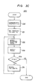
- This figure shows a detailed flow chart of the processing of correcting the base data.
- the band intervals (in the Y-axial direction) of adjacent bands which have been read from the X-ray film 3 imaged by the shotgun method and which have been normalized on the boundary line indicated by the dot-and-dash line II in Fig. 7 have a relationship shown in Fig. 8 to the values of Y-axial positions.
- the band intervals of the adjacent bands are successively found on the basis of the differences of the addresses of the area SD in which the base data items are stored, and they are compared with the minimum band interval D min in Fig. 8.
- the base data of that band of the adjacent bands used for finding the band interval as to which the value of the Y-axial position, namely, the address value of the area SD is smaller is regarded as noise and is erased from the area SD.
- the noise elimination processing stated above is performed for the whole area SD.
- the band intervals of the adjacent bands are found by successively increasing the values of the Y-axial positions, namely, the addresses.
- a band interval function BY with the characteristic of Fig. 7 moved in parallel in the Y-axial direction (lateral direction in Fig. 7) is calculated according to the obtained band intervals of the bands, and it is stored in an area B for the band interval function within the RAM 15 having corresponding addresses in the Y-axial direction, as the reference band intervals in successive fashion (step 431).
- band interval function BY is found in this way is that the values in the Y-axial direction in Fig. 7 change depending upon the placed position of the X-ray film 3 on the transparent glass 2, and so on.
- the band intervals of the adjacent bands are found by successively increasing the addresses of the area SD.
- the band interval is compared with a permissible band interval which is obtained in such a way that the reference band interval read out from the address of the area B corresponding to the value of the Y-axial position of the middle point of the adjacent bands is multiplied by a predetermined constant (step 432).
- a permissible band interval which is obtained in such a way that the reference band interval read out from the address of the area B corresponding to the value of the Y-axial position of the middle point of the adjacent bands is multiplied by a predetermined constant (step 432).
- the slopes of the bands of the respective bases A, C, G and T corresponding to the Y-axial position of a correction point which is the middle point of the adjacent bands in the area SD are found by the same process for detecting the band positions as stated before, and the values (inverse normalized correction points) of the Y-axial position for the band centers (x MA , x MC , x MG and x MT in Fig. 5B) of the respective bases A, C, G and T corresponding to the first-mentioned correction point are found.
- the value of the inverse normalized correction point of the spectrum SS MA is compared with a value equal to, e. g., 1/2 of the value of the spectrum SS MA recognized as a band near the inverse normalized correction point, and when the value of the spectrum at the inverse normalized correction point is greater, this inverse normalized correction point is deemed the band candidate point of the base A.
- the band candidate points of the respective bases C, G and T are detected as to the spectra SS MC , SS MG and SS MT . In a case where the plurality of band candidate points have been obtained in this manner, the values of the spectra at the respective band candidate points are compared.
- the base having the greatest spectral value is determined as a correction base, and correction base data is stored in the address of the area SD corresponding to the correction point.
- a decision with the condition taken into consideration is effective. For example, under the known condition that, when the adjacent band is of the base A, the value of the adjacent base C becomes 30 % smaller, or that a ghost appears (the value increases by 30 %), the comparison is made after correcting the value of the base C.
- the processing flow shifts to a step 435.
- whether or not the check of the band intervals in the whole area in the Y-axial direction is over is decided. When it is not over, the processing flow shifts to the step 432.
- the band interval check for the whole area in the Y-axial direction is executed, whereupon the processing of Fig. 3E ends.
- the base data items of the area SD within the RAM 15 are examined on the basis of the band interval characteristic known beforehand, so as to erase the base data detected erroneously and to compensate for the base data failing to be detected.
- the band interval of the adjacent bands is compared with the minimum band interval D min , and the base data of the band being noise is erased from the area SD of the memory 15. Besides, the band interval of the adjacent bands is compared with the reference band interval corresponding to the band position, and the band left undetected is re-detected to correct the band position. Therefore, failure in the band detection attributed to a thin band or a close band interval can be prevented from occurring, and band arrayal data including no error can be obtained.
- the base data items stored in the area SD of the memory 15 are read out in the order of the addresses corresponding to the Y-axial direction, so as to be stored in the disk device 16 and to be transmitted from the external interface circuit 17 to the external computer (not shown).
- band arrayal information of the bases of the gene imaged with X-rays has been described by way of example, the invention is not restricted thereto, but band arrayal information in the chromatogram of amino acids etc. may well be read. Besides, bands being moved by electrophoresis or the like may well be directly detected by a fixed sensor.
- a band arrayal pattern can be automatically read.
- the band positions of the respective lanes can be accurately detected even when the lanes are meandering.
- histograms can be obtained in parallel with the collection of density data, so that processing can be made faster.
- the arrayal order of bands can be accurately detected even when the bands incline in the individual lanes.
- the band interval of adjacent bands on the single line is compared with the minimum band interval as predetermined and a reference band interval according to a position on the single line and wherein the band is erased or re-detected, the erroneous reading of the band position can be prevented.
Landscapes
- Health & Medical Sciences (AREA)
- Life Sciences & Earth Sciences (AREA)
- Molecular Biology (AREA)
- Chemical & Material Sciences (AREA)
- General Physics & Mathematics (AREA)
- Physics & Mathematics (AREA)
- Chemical Kinetics & Catalysis (AREA)
- Spectroscopy & Molecular Physics (AREA)
- High Energy & Nuclear Physics (AREA)
- Electrochemistry (AREA)
- Analytical Chemistry (AREA)
- Biochemistry (AREA)
- General Health & Medical Sciences (AREA)
- Immunology (AREA)
- Pathology (AREA)
- Image Analysis (AREA)
- Image Processing (AREA)
Applications Claiming Priority (4)
| Application Number | Priority Date | Filing Date | Title |
|---|---|---|---|
| JP241548/85 | 1985-10-30 | ||
| JP60241548A JPH0785055B2 (ja) | 1985-10-30 | 1985-10-30 | バンド配列パタ−ン自動読取り方法および装置 |
| JP241549/85 | 1985-10-30 | ||
| JP60241549A JPH0785056B2 (ja) | 1985-10-30 | 1985-10-30 | バンド配列パタ−ンのバンド位置補正方法 |
Publications (3)
| Publication Number | Publication Date |
|---|---|
| EP0220732A2 true EP0220732A2 (de) | 1987-05-06 |
| EP0220732A3 EP0220732A3 (en) | 1989-07-19 |
| EP0220732B1 EP0220732B1 (de) | 1992-09-23 |
Family
ID=26535320
Family Applications (1)
| Application Number | Title | Priority Date | Filing Date |
|---|---|---|---|
| EP86115046A Expired EP0220732B1 (de) | 1985-10-30 | 1986-10-29 | Verfahren und Vorrichtung zur Ablesung eines Bandmusters |
Country Status (3)
| Country | Link |
|---|---|
| US (1) | US4841443A (de) |
| EP (1) | EP0220732B1 (de) |
| DE (1) | DE3686803T2 (de) |
Cited By (3)
| Publication number | Priority date | Publication date | Assignee | Title |
|---|---|---|---|---|
| EP0483460A1 (de) * | 1990-10-30 | 1992-05-06 | Shimadzu Corporation | Vorrichtung zur Bestimmung der Basensequenz |
| WO1994020844A1 (en) * | 1993-03-09 | 1994-09-15 | Inopsia Bron & Co. | Method for automatically correcting and matching digitized electrophoresis and western blots tests |
| WO1997034164A1 (en) * | 1996-03-14 | 1997-09-18 | Simage Oy | Autoradiography imaging |
Families Citing this family (9)
| Publication number | Priority date | Publication date | Assignee | Title |
|---|---|---|---|---|
| JPS6285862A (ja) * | 1985-10-11 | 1987-04-20 | Fuji Photo Film Co Ltd | 核酸の塩基配列決定のための信号処理方法 |
| US5502773A (en) * | 1991-09-20 | 1996-03-26 | Vanderbilt University | Method and apparatus for automated processing of DNA sequence data |
| JPH07318534A (ja) * | 1994-05-27 | 1995-12-08 | Fuji Photo Film Co Ltd | 生体高分子物質の分離展開データのサンプリング方法 |
| US5800993A (en) * | 1994-07-29 | 1998-09-01 | The Regents Of The University Of California | DNA sequencing apparatus and method for a small format gel with a magnified readout |
| US5666435A (en) * | 1994-12-09 | 1997-09-09 | Genomyx Corporation | System for analysis of x-ray films of nucleotide sequences |
| US5717602A (en) * | 1996-02-05 | 1998-02-10 | Kenning; Gregory G. | Automated electrophoresis and analysis system |
| AU2001247275A1 (en) * | 2000-03-06 | 2001-09-17 | Gene Logic, Inc. | Virtual gel profiling system |
| WO2019126693A1 (en) | 2017-12-22 | 2019-06-27 | Quest Diagnostics Investments Llc | Automated analysis of analytical gels and blots |
| CN116124716B (zh) * | 2022-12-22 | 2026-02-17 | 中国科学院西安光学精密机械研究所 | 基于近感高光谱的水质监测方法及装置 |
Family Cites Families (3)
| Publication number | Priority date | Publication date | Assignee | Title |
|---|---|---|---|---|
| US3932839A (en) * | 1974-04-24 | 1976-01-13 | Stephens Richard G | Pattern analysis apparatus and method |
| EP0151974A3 (de) * | 1984-01-27 | 1987-05-06 | E.I. Du Pont De Nemours And Company | Bildelementquantisierung |
| DE3573667D1 (en) * | 1984-04-27 | 1989-11-16 | Hitachi Software Eng | Input apparatus for entering base sequence information of the gene |
-
1986
- 1986-10-29 EP EP86115046A patent/EP0220732B1/de not_active Expired
- 1986-10-29 DE DE8686115046T patent/DE3686803T2/de not_active Expired - Fee Related
- 1986-10-30 US US06/924,788 patent/US4841443A/en not_active Expired - Fee Related
Cited By (4)
| Publication number | Priority date | Publication date | Assignee | Title |
|---|---|---|---|---|
| EP0483460A1 (de) * | 1990-10-30 | 1992-05-06 | Shimadzu Corporation | Vorrichtung zur Bestimmung der Basensequenz |
| WO1994020844A1 (en) * | 1993-03-09 | 1994-09-15 | Inopsia Bron & Co. | Method for automatically correcting and matching digitized electrophoresis and western blots tests |
| WO1997034164A1 (en) * | 1996-03-14 | 1997-09-18 | Simage Oy | Autoradiography imaging |
| US6268605B1 (en) | 1996-03-14 | 2001-07-31 | Simage Oy | Autoradiography imaging |
Also Published As
| Publication number | Publication date |
|---|---|
| EP0220732A3 (en) | 1989-07-19 |
| US4841443A (en) | 1989-06-20 |
| EP0220732B1 (de) | 1992-09-23 |
| DE3686803D1 (de) | 1992-10-29 |
| DE3686803T2 (de) | 1993-05-06 |
Similar Documents
| Publication | Publication Date | Title |
|---|---|---|
| EP0220732B1 (de) | Verfahren und Vorrichtung zur Ablesung eines Bandmusters | |
| US4162482A (en) | Pre-processing and feature extraction system for character recognition | |
| US4885697A (en) | Method of identifying spectra | |
| US6151423A (en) | Character recognition with document orientation determination | |
| US4034343A (en) | Optical character recognition system | |
| US5590220A (en) | Bending point extraction method for optical character recognition system | |
| EP0184775A2 (de) | Umwandlung von einem ein Bild darstellenden Grauwertpixelfeld in ein Binärwertpixelfeld | |
| US4837733A (en) | Signal processing method in autoradiography | |
| US4180799A (en) | Apparatus and method for recognizing characters | |
| GB1567287A (en) | Pattern encoding apparatus | |
| JPH0757051A (ja) | パターン認識装置 | |
| US7085432B2 (en) | Edge detection using Hough transformation | |
| EP0240729A2 (de) | Verfahren zur autoradiographischen Untersuchung des Grundaufbaus von Nukleinsäuren | |
| US20090022405A1 (en) | System and method for video object identification | |
| US3662341A (en) | Video-derived segmentation-gating apparatus for optical character recognition | |
| EP1729505A1 (de) | Verfahren zum Separieren eines Strahlungsbereichs aus Bilddaten und Vorrichtung zur Bilddatenverarbeitung | |
| US4490852A (en) | Image capturing apparatus | |
| US20060138306A1 (en) | Method and sensing device for motion detection in an optical pointing device, such as an optical mouse | |
| JPH0785055B2 (ja) | バンド配列パタ−ン自動読取り方法および装置 | |
| JPH0785056B2 (ja) | バンド配列パタ−ンのバンド位置補正方法 | |
| US4868749A (en) | Signal processing method in autoradiography | |
| EP0113678A2 (de) | Signalbearbeitungsmethode in der Autoradiographie | |
| US6260764B1 (en) | Method of detecting a bar code on a scan line, and an apparatus for detecting and decoding a bar code | |
| JP2576370B2 (ja) | Idマーク読み取り装置 | |
| US20050135702A1 (en) | Methods, systems and computer software for detecting pixel stutter |
Legal Events
| Date | Code | Title | Description |
|---|---|---|---|
| PUAI | Public reference made under article 153(3) epc to a published international application that has entered the european phase |
Free format text: ORIGINAL CODE: 0009012 |
|
| AK | Designated contracting states |
Kind code of ref document: A2 Designated state(s): DE FR GB SE |
|
| PUAL | Search report despatched |
Free format text: ORIGINAL CODE: 0009013 |
|
| AK | Designated contracting states |
Kind code of ref document: A3 Designated state(s): DE FR GB SE |
|
| 17P | Request for examination filed |
Effective date: 19900105 |
|
| 17Q | First examination report despatched |
Effective date: 19910415 |
|
| GRAA | (expected) grant |
Free format text: ORIGINAL CODE: 0009210 |
|
| AK | Designated contracting states |
Kind code of ref document: B1 Designated state(s): DE FR GB SE |
|
| REF | Corresponds to: |
Ref document number: 3686803 Country of ref document: DE Date of ref document: 19921029 |
|
| ET | Fr: translation filed | ||
| PLBE | No opposition filed within time limit |
Free format text: ORIGINAL CODE: 0009261 |
|
| STAA | Information on the status of an ep patent application or granted ep patent |
Free format text: STATUS: NO OPPOSITION FILED WITHIN TIME LIMIT |
|
| 26N | No opposition filed | ||
| EAL | Se: european patent in force in sweden |
Ref document number: 86115046.4 |
|
| PGFP | Annual fee paid to national office [announced via postgrant information from national office to epo] |
Ref country code: SE Payment date: 19971013 Year of fee payment: 12 |
|
| PGFP | Annual fee paid to national office [announced via postgrant information from national office to epo] |
Ref country code: GB Payment date: 19971017 Year of fee payment: 12 Ref country code: FR Payment date: 19971017 Year of fee payment: 12 |
|
| PGFP | Annual fee paid to national office [announced via postgrant information from national office to epo] |
Ref country code: DE Payment date: 19971223 Year of fee payment: 12 |
|
| PG25 | Lapsed in a contracting state [announced via postgrant information from national office to epo] |
Ref country code: GB Free format text: LAPSE BECAUSE OF NON-PAYMENT OF DUE FEES Effective date: 19981029 |
|
| PG25 | Lapsed in a contracting state [announced via postgrant information from national office to epo] |
Ref country code: SE Free format text: LAPSE BECAUSE OF NON-PAYMENT OF DUE FEES Effective date: 19981030 |
|
| GBPC | Gb: european patent ceased through non-payment of renewal fee |
Effective date: 19981029 |
|
| EUG | Se: european patent has lapsed |
Ref document number: 86115046.4 |
|
| PG25 | Lapsed in a contracting state [announced via postgrant information from national office to epo] |
Ref country code: FR Free format text: LAPSE BECAUSE OF NON-PAYMENT OF DUE FEES Effective date: 19990630 |
|
| REG | Reference to a national code |
Ref country code: FR Ref legal event code: ST |
|
| PG25 | Lapsed in a contracting state [announced via postgrant information from national office to epo] |
Ref country code: DE Free format text: LAPSE BECAUSE OF NON-PAYMENT OF DUE FEES Effective date: 19990803 |