EP0220856A2 - Tampon d'entrée source-suiveur CMOS - Google Patents
Tampon d'entrée source-suiveur CMOS Download PDFInfo
- Publication number
- EP0220856A2 EP0220856A2 EP86307708A EP86307708A EP0220856A2 EP 0220856 A2 EP0220856 A2 EP 0220856A2 EP 86307708 A EP86307708 A EP 86307708A EP 86307708 A EP86307708 A EP 86307708A EP 0220856 A2 EP0220856 A2 EP 0220856A2
- Authority
- EP
- European Patent Office
- Prior art keywords
- transistor
- circuit
- output
- source
- source follower
- Prior art date
- Legal status (The legal status is an assumption and is not a legal conclusion. Google has not performed a legal analysis and makes no representation as to the accuracy of the status listed.)
- Granted
Links
- 230000005669 field effect Effects 0.000 claims abstract description 7
- 239000004065 semiconductor Substances 0.000 claims description 3
- 230000008878 coupling Effects 0.000 claims 1
- 238000010168 coupling process Methods 0.000 claims 1
- 238000005859 coupling reaction Methods 0.000 claims 1
- 230000007704 transition Effects 0.000 description 6
- 230000008901 benefit Effects 0.000 description 2
- 230000000630 rising effect Effects 0.000 description 2
- 239000003990 capacitor Substances 0.000 description 1
- 230000001934 delay Effects 0.000 description 1
- 230000015654 memory Effects 0.000 description 1
- 230000004048 modification Effects 0.000 description 1
- 238000012986 modification Methods 0.000 description 1
- 235000013599 spices Nutrition 0.000 description 1
Images
Classifications
-
- H—ELECTRICITY
- H03—ELECTRONIC CIRCUITRY
- H03K—PULSE TECHNIQUE
- H03K19/00—Logic circuits, i.e. having at least two inputs acting on one output; Inverting circuits
- H03K19/02—Logic circuits, i.e. having at least two inputs acting on one output; Inverting circuits using specified components
- H03K19/08—Logic circuits, i.e. having at least two inputs acting on one output; Inverting circuits using specified components using semiconductor devices
- H03K19/094—Logic circuits, i.e. having at least two inputs acting on one output; Inverting circuits using specified components using semiconductor devices using field-effect transistors
- H03K19/0944—Logic circuits, i.e. having at least two inputs acting on one output; Inverting circuits using specified components using semiconductor devices using field-effect transistors using MOSFET or insulated gate field-effect transistors, i.e. IGFET
- H03K19/0948—Logic circuits, i.e. having at least two inputs acting on one output; Inverting circuits using specified components using semiconductor devices using field-effect transistors using MOSFET or insulated gate field-effect transistors, i.e. IGFET using CMOS or complementary insulated gate field-effect transistors
-
- H—ELECTRICITY
- H03—ELECTRONIC CIRCUITRY
- H03K—PULSE TECHNIQUE
- H03K19/00—Logic circuits, i.e. having at least two inputs acting on one output; Inverting circuits
- H03K19/01—Modifications for accelerating switching
- H03K19/017—Modifications for accelerating switching in field-effect transistor circuits
- H03K19/01707—Modifications for accelerating switching in field-effect transistor circuits in asynchronous circuits
- H03K19/01721—Modifications for accelerating switching in field-effect transistor circuits in asynchronous circuits by means of a pull-up or down element
-
- H—ELECTRICITY
- H03—ELECTRONIC CIRCUITRY
- H03K—PULSE TECHNIQUE
- H03K19/00—Logic circuits, i.e. having at least two inputs acting on one output; Inverting circuits
- H03K19/0175—Coupling arrangements; Interface arrangements
- H03K19/0185—Coupling arrangements; Interface arrangements using field effect transistors only
- H03K19/018507—Interface arrangements
- H03K19/018521—Interface arrangements of complementary type, e.g. CMOS
Definitions
- the present invention relates to an input circuit for use preferably in a CMOS semiconductor memory.
- An input buffer for a semiconductor memory should be able to receive a TTL input signal (being in the range of 0.8 to 2.0 volts) and generate an output signal in a voltage range corresponding to the chip (generally between VSS and VCC), which in the case of CMOS memories today is 0 volts to 5 volts. Another requirement is that the input buffer must be able to drive high internal chip capacitances.
- the problem which is solved by the present invention will be understood from consideration of the conventional input buffer circuit illustrated in Figure 1 and its shortcomings.
- the problem with the circuit of Figure 1 concerns the compromise made between speed of operation and standby current. As will be explained, these have been mutually inconsistent goals, i.e. to achieve increased speed, one sacrifices standby current.
- the present invention overcomes this problem.
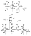
- FIG. 1 shows a conventional CMOS input buffer circuit 10 formed of field effect transistors (FETs) which are all enhancement mode devices.
- Circuit 10 receives an input at 12 and applies it to a first inverter stage 14 comprising a CMOS pair of transistors 16, 18.
- Device 16 is a p-channel device, whereas device 18 is an n-channel device.
- the source-drain paths of transistors 16, 18 are connected in series between VCC and ground, as illustrated.
- Input 12 is coupled to the gate electrodes of each of these transistors.
- a node A between the source of transistor 16 and the drain of transistor 18 provides an input to the second stage inverter 20.
- Inverter 20 comprises another pair of CMOS transistors including transistors 24 and 26 connected in a fashion identical to stage 14.
- the output node B of stage 22 is provided to the capacitive load of the chip as represented by capacitor 28.
- transistors 16 and 18 will both be turned on. Current will flow from VCC to ground through the source-drain paths of these transistors.
- Transistors 18 will be sized approximately four or five times larger than transistor 16 in order to insure that the voltage at node A is at or near ground when the input voltage is at a TTL logic "1" level of about 2.0 volts. In actuality, the voltage at node A may be about 1.0 volts at this condition, and as a result, some current will flow in the second stage 20.
- the output of inverter stage 20 will have the same logic value as input 12.
- the transistors in output stage 20 will need a channel width typically of about 200 microns, using a guideline of about 40 microns per pf for an n-channel transistor. This is a fairly large transistor, and the transistors in the first stage 14 must be large because node A must drive each of transistors 24 and 26.
- the current through the first stage will be significant. To reduce this standby current, more inverter stages could be added. This would allow downsizing the transistors in the first stage. However, adding stages will increase the delay in the transitions in the input and the output. This undesirable result is overcome by the present invention.
- the present invention in one embodiment uses a CMOS inverter input stage coupled to drive primarily an n-channel pull-up transistor connected as a source follower whose output drives a CMOS output inverter stage.
- a subsidiary feature of the present invention is the use of a small p-channel transistor cooperating with the n-channel source follower transistor to assure that a full VCC level is achieved at the output of the pull-up n-channel device.
- the advantage of this circuit is that regardless of whether a TTL or CMOS voltage level is applied at the input, the circuit according to this invention will have low standby current. Additionally, if one allows the circuit according to the present invention to draw the same current as the circuit of Figure 1, there will be an improvement in speed of the current. On the other hand, if one configures the circuit elements to achieve the same speed, a circuit according to the present invention will use about one-half the current of the circuit of Figure 1.
- FIG. 2 illustrates a circuit 30 according to the present invention.
- Circuit 30 receives an input at 32 and applies it to an input stage 34 which comprises transistors 36 and 38 which are enhancement mode devices, as are all of the other transistors illustrated in Figure 2.
- Transistor 36 is a p-channel device and transistor 38 preferably is its corresponding n-channel device.
- Transistors 36, 38 form a CMOS pair.
- the source-drain paths of transistors 36 and 38 are coupled in series between VCC and ground.
- An output 40 of inverter stage 34 is applied to the gate electrodes of an n-channel transistor 42 and a CMOS pair of transistors 44, 46.
- the channel width of transistors 44, 46 is small, illustratively 6 microns, whereas the width of n-channel transistor 42 illustratively will be about 120 microns.
- the source-drain path of transistor 42 is coupled at the drain to VCC and at the source to a node C.
- a further transistor 48 is also an n-channel device whose souce-drain path couples node C to ground.
- the gate electrode of transistor 48 is not, however, coupled to node 40, but instead is driven by the input 32.
- transistor 42 coupled as a source follower to the first inverter stage, provides substantial pull-up to enable node C to drive more capacitance than node 40 would be able to drive.
- the delay between a rising transition at node 40 and the rising transition at node C will be small because transistor 42 is connected as a source follower.
- node C closely follows node 40 because source follower transistor 42 is large and has a high gain.
- Node C drives an output inverter stage and is coupled to the gate electrode of a CMOS pair of transistors 50 and 52 whose source-drain paths are coupled in series between VCC and ground.
- a node D between the source of transistor 50 and the drain of transistor 52 provides the output to the capacitive load 54.
- n-channel transistor has more gain than a p-channel transistor of the same size.
- transistors 50 and 52 in the output stage can be made larger than otherwise obtainable by the prior art circuit of Figure 1.
- the larger width of transistors at this output stage will result in this stage having a faster operation than otherwise obtainable.
- the source follower transistor 42 is an n-channel device. As such, it cannot pull up all the way to VCC, but instead rises to one voltage transistion lower than VCC. To allow the voltage at node C to rise all the way to VCC, it is preferred to include a p-channel transistor 56 having its drain coupled to VCC and its source coupled to node C. This device is not added for speed, but only to ensure that the voltage rises fully at node C. Thus, it can be a small transistor, having a channel width illustratively of 6 microns. It does not affect the delay between the input 32 and output node D.
- Transistors 44 and 46 provide an inverter stage to allow the voltage at its output node E, which is coupled to the gate electrode of transistor 56, to be the logic inverse of the state of node 40.
- Transistors 44, 46 can be small, illustratively with a channel width of six microns, and the current drawn by them is correspondingly small.
- Transistor 48 is included in the preferred embodiment to insure that when the input voltage at 32 is 2.0 volts, node C will be pulled all the way to ground.
- transistor 48 is an n-channel device which is gated by the input voltage on 32.
- the source-drain path of transistor 48 will insure that node C drops to ground during this conditon.
- the benefit of this is that if the input voltage at 32 is at a TTL logic high of 2.0 volts, then the 0 volts at node C will insure that CMOS pair 50, 52 of the output inverter stage will draw no current.
- the operation of the circuit of Figure 2 ensures that the voltage at node C will either be ground (VSS) or VCC when the input voltage is high or low. Because of this, either transistor 50 or 52 will be off so there is no standby current consumed at the output stage.
- a p-channel device has about one-half of the gain of an n-channel device of the same width.
- the gain on pull-up of CMOS pair connected as an inverter would be about one-third the gain of transistor 42, keeping the total channel width constant.
- the result of using an n-channel transistor rather than a CMOS inverter pair is to improve the pull-up by a factor of three.
- transistor 36 can have a width of 24 and a length of 4; transistor 38 can have a width of 120 and a length of 3.5; transistor 48 can have a width of 80; transistor 50 can have a width of 120; and transistor 22 can have a width of 240 (all expressed in microns).
- Transistor 48 could be eliminated, if one were content to allow the output stage to draw higher standby current.
- transistors 44, 46 and 56 can be eliminated with the same result.
- Other variations, modifications and embellishments can be made within the scope of this invention.
Landscapes
- Engineering & Computer Science (AREA)
- Computer Hardware Design (AREA)
- Physics & Mathematics (AREA)
- Computing Systems (AREA)
- General Engineering & Computer Science (AREA)
- Mathematical Physics (AREA)
- Power Engineering (AREA)
- Logic Circuits (AREA)
- Metal-Oxide And Bipolar Metal-Oxide Semiconductor Integrated Circuits (AREA)
Applications Claiming Priority (2)
| Application Number | Priority Date | Filing Date | Title |
|---|---|---|---|
| US06/788,442 US4698526A (en) | 1985-10-17 | 1985-10-17 | Source follower CMOS input buffer |
| US788442 | 1985-10-17 |
Publications (3)
| Publication Number | Publication Date |
|---|---|
| EP0220856A2 true EP0220856A2 (fr) | 1987-05-06 |
| EP0220856A3 EP0220856A3 (en) | 1988-10-26 |
| EP0220856B1 EP0220856B1 (fr) | 1993-12-29 |
Family
ID=25144503
Family Applications (1)
| Application Number | Title | Priority Date | Filing Date |
|---|---|---|---|
| EP86307708A Expired - Lifetime EP0220856B1 (fr) | 1985-10-17 | 1986-10-06 | Tampon d'entrée source-suiveur CMOS |
Country Status (4)
| Country | Link |
|---|---|
| US (1) | US4698526A (fr) |
| EP (1) | EP0220856B1 (fr) |
| JP (1) | JPS62169359A (fr) |
| DE (1) | DE3689466T2 (fr) |
Cited By (4)
| Publication number | Priority date | Publication date | Assignee | Title |
|---|---|---|---|---|
| EP0313810A3 (fr) * | 1987-10-30 | 1989-09-06 | International Business Machines Corporation | Circuit récepteur du type source-suiveur pour signaux ECL |
| EP0403075A3 (fr) * | 1989-05-15 | 1991-07-03 | Texas Instruments Incorporated | Circuit logique BICMOS à haut rendement avec oscillation complète de la tension de sortie |
| GB2252213A (en) * | 1991-01-22 | 1992-07-29 | Samsung Electronics Co Ltd | TTL input buffer |
| EP0368742B1 (fr) * | 1988-11-08 | 1998-02-04 | Bull S.A. | Amplificateur binaire intégré et circuit intégré l'incorporant |
Families Citing this family (25)
| Publication number | Priority date | Publication date | Assignee | Title |
|---|---|---|---|---|
| JPH0817028B2 (ja) * | 1985-12-06 | 1996-02-21 | 日本電気株式会社 | リフレッシュ信号入力回路 |
| US4737667A (en) * | 1986-03-11 | 1988-04-12 | Siemens Aktiengesellschaft | Driving circuitry for a MOSFET having a source load |
| IT1201859B (it) * | 1986-12-10 | 1989-02-02 | Sgs Microelettronica Spa | Circuito logico cmos |
| US4916334A (en) * | 1987-07-29 | 1990-04-10 | Kabushiki Kaisha Toshiba | High voltage booster circuit for use in EEPROMs |
| US4958093A (en) * | 1989-05-25 | 1990-09-18 | International Business Machines Corporation | Voltage clamping circuits with high current capability |
| US4988897A (en) * | 1989-05-27 | 1991-01-29 | Samsung Electronics, Co., Ltd. | TTL to CMOS input buffer circuit |
| US4968905A (en) * | 1989-08-25 | 1990-11-06 | Ncr Corporation | Temperature compensated high speed ECL-to-CMOS logic level translator |
| US5019728A (en) * | 1990-09-10 | 1991-05-28 | Ncr Corporation | High speed CMOS backpanel transceiver |
| US5151622A (en) * | 1990-11-06 | 1992-09-29 | Vitelic Corporation | CMOS logic circuit with output coupled to multiple feedback paths and associated method |
| US5115150A (en) * | 1990-11-19 | 1992-05-19 | Hewlett-Packard Co. | Low power CMOS bus receiver with small setup time |
| US5247212A (en) * | 1991-01-31 | 1993-09-21 | Thunderbird Technologies, Inc. | Complementary logic input parallel (clip) logic circuit family |
| US5172016A (en) * | 1991-06-28 | 1992-12-15 | Digital Equipment Corporation | Five-volt tolerant differential receiver |
| US5321324A (en) * | 1993-01-28 | 1994-06-14 | United Memories, Inc. | Low-to-high voltage translator with latch-up immunity |
| US6104229A (en) * | 1996-05-02 | 2000-08-15 | Integrated Device Technology, Inc. | High voltage tolerable input buffer and method for operating same |
| US5914681A (en) * | 1997-10-02 | 1999-06-22 | Burr-Brown Corporation | Fast wakeup biasing circuit for analog-to-digital converter |
| US5914844A (en) * | 1997-10-14 | 1999-06-22 | Cypress Semiconductor Corp. | Overvoltage-tolerant input-output buffers having a switch configured to isolate a pull up transistor from a voltage supply |
| US6049242A (en) | 1997-10-14 | 2000-04-11 | Cypress Semiconductor Corp. | Voltage reference source for an overvoltage-tolerant bus interface |
| US6496033B2 (en) | 1998-06-08 | 2002-12-17 | Cypress Semiconductor Corp. | Universal logic chip |
| US6496054B1 (en) | 2000-05-13 | 2002-12-17 | Cypress Semiconductor Corp. | Control signal generator for an overvoltage-tolerant interface circuit on a low voltage process |
| US6469562B1 (en) * | 2000-06-26 | 2002-10-22 | Jun-Ren Shih | Source follower with Vgs compensation |
| US8018268B1 (en) | 2004-11-19 | 2011-09-13 | Cypress Semiconductor Corporation | Over-voltage tolerant input circuit |
| JP5008032B2 (ja) | 2007-08-30 | 2012-08-22 | ソニーモバイルディスプレイ株式会社 | 遅延回路、半導体制御回路、表示装置、および電子機器 |
| US20100321083A1 (en) * | 2009-06-22 | 2010-12-23 | International Business Machines Corporation | Voltage Level Translating Circuit |
| KR101067197B1 (ko) * | 2009-12-15 | 2011-09-22 | 삼성전기주식회사 | 이동통신 단말기의 전력증폭모듈 |
| CN102931972B (zh) * | 2012-11-14 | 2014-12-24 | 中国电子科技集团公司第二十四研究所 | Cmos输入缓冲器 |
Family Cites Families (10)
| Publication number | Priority date | Publication date | Assignee | Title |
|---|---|---|---|---|
| US4217502A (en) * | 1977-09-10 | 1980-08-12 | Tokyo Shibaura Denki Kabushiki Kaisha | Converter producing three output states |
| US4176289A (en) * | 1978-06-23 | 1979-11-27 | Electronic Memories & Magnetics Corporation | Driving circuit for integrated circuit semiconductor memory |
| US4365172A (en) * | 1980-01-11 | 1982-12-21 | Texas Instruments Incorporated | High current static MOS driver circuit with low DC power dissipation |
| JPS56140726A (en) * | 1980-04-02 | 1981-11-04 | Toshiba Corp | Output circuit |
| EP0058958B1 (fr) * | 1981-02-25 | 1986-10-29 | Kabushiki Kaisha Toshiba | Circuit logique du type MOSFET complémentaire |
| JPS57203334A (en) * | 1981-06-08 | 1982-12-13 | Mitsubishi Electric Corp | Semiconductor integrated circuit device |
| US4498021A (en) * | 1982-07-13 | 1985-02-05 | Matsushita Electric Industrial Co., Ltd. | Booster for transmitting digital signal |
| JPS59200326A (ja) * | 1983-04-26 | 1984-11-13 | Nec Corp | データ処理装置 |
| US4549101A (en) * | 1983-12-01 | 1985-10-22 | Motorola, Inc. | Circuit for generating test equalization pulse |
| US4593212A (en) * | 1984-12-28 | 1986-06-03 | Motorola, Inc. | TTL to CMOS input buffer |
-
1985
- 1985-10-17 US US06/788,442 patent/US4698526A/en not_active Expired - Lifetime
-
1986
- 1986-10-06 DE DE3689466T patent/DE3689466T2/de not_active Expired - Fee Related
- 1986-10-06 EP EP86307708A patent/EP0220856B1/fr not_active Expired - Lifetime
- 1986-10-16 JP JP61244331A patent/JPS62169359A/ja active Pending
Cited By (4)
| Publication number | Priority date | Publication date | Assignee | Title |
|---|---|---|---|---|
| EP0313810A3 (fr) * | 1987-10-30 | 1989-09-06 | International Business Machines Corporation | Circuit récepteur du type source-suiveur pour signaux ECL |
| EP0368742B1 (fr) * | 1988-11-08 | 1998-02-04 | Bull S.A. | Amplificateur binaire intégré et circuit intégré l'incorporant |
| EP0403075A3 (fr) * | 1989-05-15 | 1991-07-03 | Texas Instruments Incorporated | Circuit logique BICMOS à haut rendement avec oscillation complète de la tension de sortie |
| GB2252213A (en) * | 1991-01-22 | 1992-07-29 | Samsung Electronics Co Ltd | TTL input buffer |
Also Published As
| Publication number | Publication date |
|---|---|
| DE3689466T2 (de) | 1994-07-28 |
| JPS62169359A (ja) | 1987-07-25 |
| EP0220856B1 (fr) | 1993-12-29 |
| EP0220856A3 (en) | 1988-10-26 |
| DE3689466D1 (de) | 1994-02-10 |
| US4698526A (en) | 1987-10-06 |
Similar Documents
| Publication | Publication Date | Title |
|---|---|---|
| US4698526A (en) | Source follower CMOS input buffer | |
| EP0493873B1 (fr) | Circuit tampon de sortie CMOS avec réduction des transitoires dans les lignes de masse | |
| JP2922028B2 (ja) | 半導体集積回路の出力回路 | |
| US5073726A (en) | Input circuit of semiconductor integrated circuit and semiconductor integrated circuit having input circuit | |
| US6351421B1 (en) | Data output buffer | |
| US5121000A (en) | Edge-rate feedback CMOS output buffer circuits | |
| US5313118A (en) | High-speed, low-noise, CMOS output driver | |
| JPS6010812A (ja) | ドライバ回路 | |
| EP0196113B1 (fr) | Circuit tampon à trois états | |
| JP2535082B2 (ja) | 双極性相補形金属酸化物半導体出力駆動回路 | |
| US4386286A (en) | High current static MOS output buffer circuit for power-down mode of operation | |
| US4395645A (en) | Mosfet logic inverter buffer circuit for integrated circuits | |
| US4918332A (en) | TTL output driver gate configuration | |
| US5402081A (en) | Input buffer circuit with improved speed performance | |
| US5359240A (en) | Low power digital signal buffer circuit | |
| US5045722A (en) | Output buffer preconditioning circuit | |
| JPH09200036A (ja) | 論理回路及びこれを用いた半導体集積回路 | |
| US5442304A (en) | CMOS logic gate clamping circuit | |
| JPH0440893B2 (fr) | ||
| CA1157919A (fr) | Circuit-tampon | |
| US6175598B1 (en) | Output noise control scheme for multiple I/O's | |
| US5576639A (en) | BICMOS level shifter of a semiconductor integrated circuit and data output buffer using the same | |
| JPH05291939A (ja) | Cmosセルフブースト回路 | |
| JP3201020B2 (ja) | ラッチ回路 | |
| JP2611543B2 (ja) | Mosトランジスタ出力回路 |
Legal Events
| Date | Code | Title | Description |
|---|---|---|---|
| PUAI | Public reference made under article 153(3) epc to a published international application that has entered the european phase |
Free format text: ORIGINAL CODE: 0009012 |
|
| AK | Designated contracting states |
Kind code of ref document: A2 Designated state(s): DE FR GB NL |
|
| PUAL | Search report despatched |
Free format text: ORIGINAL CODE: 0009013 |
|
| AK | Designated contracting states |
Kind code of ref document: A3 Designated state(s): DE FR GB NL |
|
| 17P | Request for examination filed |
Effective date: 19890210 |
|
| 17Q | First examination report despatched |
Effective date: 19890913 |
|
| RAP1 | Party data changed (applicant data changed or rights of an application transferred) |
Owner name: THORN EMI NORTH AMERICA INC. |
|
| GRAA | (expected) grant |
Free format text: ORIGINAL CODE: 0009210 |
|
| AK | Designated contracting states |
Kind code of ref document: B1 Designated state(s): DE FR GB NL |
|
| REF | Corresponds to: |
Ref document number: 3689466 Country of ref document: DE Date of ref document: 19940210 |
|
| ET | Fr: translation filed | ||
| PLBE | No opposition filed within time limit |
Free format text: ORIGINAL CODE: 0009261 |
|
| STAA | Information on the status of an ep patent application or granted ep patent |
Free format text: STATUS: NO OPPOSITION FILED WITHIN TIME LIMIT |
|
| 26N | No opposition filed | ||
| REG | Reference to a national code |
Ref country code: GB Ref legal event code: IF02 |
|
| PGFP | Annual fee paid to national office [announced via postgrant information from national office to epo] |
Ref country code: FR Payment date: 20020923 Year of fee payment: 17 |
|
| PGFP | Annual fee paid to national office [announced via postgrant information from national office to epo] |
Ref country code: GB Payment date: 20020926 Year of fee payment: 17 |
|
| PGFP | Annual fee paid to national office [announced via postgrant information from national office to epo] |
Ref country code: NL Payment date: 20021003 Year of fee payment: 17 |
|
| PGFP | Annual fee paid to national office [announced via postgrant information from national office to epo] |
Ref country code: DE Payment date: 20021205 Year of fee payment: 17 |
|
| PG25 | Lapsed in a contracting state [announced via postgrant information from national office to epo] |
Ref country code: GB Free format text: LAPSE BECAUSE OF NON-PAYMENT OF DUE FEES Effective date: 20031006 |
|
| PG25 | Lapsed in a contracting state [announced via postgrant information from national office to epo] |
Ref country code: NL Free format text: LAPSE BECAUSE OF NON-PAYMENT OF DUE FEES Effective date: 20040501 Ref country code: DE Free format text: LAPSE BECAUSE OF NON-PAYMENT OF DUE FEES Effective date: 20040501 |
|
| GBPC | Gb: european patent ceased through non-payment of renewal fee |
Effective date: 20031006 |
|
| PG25 | Lapsed in a contracting state [announced via postgrant information from national office to epo] |
Ref country code: FR Free format text: LAPSE BECAUSE OF NON-PAYMENT OF DUE FEES Effective date: 20040630 |
|
| NLV4 | Nl: lapsed or anulled due to non-payment of the annual fee |
Effective date: 20040501 |
|
| REG | Reference to a national code |
Ref country code: FR Ref legal event code: ST |