EP0222593A2 - Digitale Filter und Demodulatoren - Google Patents
Digitale Filter und Demodulatoren Download PDFInfo
- Publication number
- EP0222593A2 EP0222593A2 EP86308627A EP86308627A EP0222593A2 EP 0222593 A2 EP0222593 A2 EP 0222593A2 EP 86308627 A EP86308627 A EP 86308627A EP 86308627 A EP86308627 A EP 86308627A EP 0222593 A2 EP0222593 A2 EP 0222593A2
- Authority
- EP
- European Patent Office
- Prior art keywords
- signal
- digital
- symbol timing
- symbol
- phase
- Prior art date
- Legal status (The legal status is an assumption and is not a legal conclusion. Google has not performed a legal analysis and makes no representation as to the accuracy of the status listed.)
- Granted
Links
- 238000011084 recovery Methods 0.000 claims abstract description 21
- 230000004044 response Effects 0.000 claims abstract description 17
- 238000012937 correction Methods 0.000 claims abstract description 14
- 230000001934 delay Effects 0.000 claims abstract description 11
- 238000005070 sampling Methods 0.000 claims description 8
- 230000000694 effects Effects 0.000 claims description 5
- 238000001914 filtration Methods 0.000 claims description 4
- 230000006870 function Effects 0.000 description 12
- 238000010586 diagram Methods 0.000 description 8
- 230000010363 phase shift Effects 0.000 description 6
- 238000012545 processing Methods 0.000 description 5
- 238000000034 method Methods 0.000 description 4
- 238000007476 Maximum Likelihood Methods 0.000 description 3
- 230000035945 sensitivity Effects 0.000 description 2
- 238000000926 separation method Methods 0.000 description 2
- 238000001228 spectrum Methods 0.000 description 2
- 230000007704 transition Effects 0.000 description 2
- 238000012935 Averaging Methods 0.000 description 1
- 230000008859 change Effects 0.000 description 1
- 230000001419 dependent effect Effects 0.000 description 1
- 238000013461 design Methods 0.000 description 1
- 230000008569 process Effects 0.000 description 1
- 230000009467 reduction Effects 0.000 description 1
- 230000008929 regeneration Effects 0.000 description 1
- 238000011069 regeneration method Methods 0.000 description 1
- 230000003252 repetitive effect Effects 0.000 description 1
Images

Classifications
-
- H—ELECTRICITY
- H04—ELECTRIC COMMUNICATION TECHNIQUE
- H04L—TRANSMISSION OF DIGITAL INFORMATION, e.g. TELEGRAPHIC COMMUNICATION
- H04L7/00—Arrangements for synchronising receiver with transmitter
- H04L7/0054—Detection of the synchronisation error by features other than the received signal transition
- H04L7/007—Detection of the synchronisation error by features other than the received signal transition detection of error based on maximum signal power, e.g. peak value, maximizing autocorrelation
-
- H—ELECTRICITY
- H04—ELECTRIC COMMUNICATION TECHNIQUE
- H04L—TRANSMISSION OF DIGITAL INFORMATION, e.g. TELEGRAPHIC COMMUNICATION
- H04L7/00—Arrangements for synchronising receiver with transmitter
- H04L7/0016—Arrangements for synchronising receiver with transmitter correction of synchronization errors
- H04L7/002—Arrangements for synchronising receiver with transmitter correction of synchronization errors correction by interpolation
- H04L7/0029—Arrangements for synchronising receiver with transmitter correction of synchronization errors correction by interpolation interpolation of received data signal
Definitions
- the present invention relates to a demodulator for demodulating a signal which is for example Pulse Amplitude Modulated or Quadrature Amplitude Modulated.
- a demodulator for demodulating a signal which is for example Pulse Amplitude Modulated or Quadrature Amplitude Modulated.
- it relates to digital filters, especially but not exclusively, for use in such a demodulator.
- a demodulator for demodulating a signal the demodulator comprising: means for producing a digital representation of the modulated signal, a digital symbol timing recovery and correction circuit responsive to the said digital representation for producing a digital signal indicative of symbol timing and for correcting symbol timing in dependence on the indicative signal, and digital demodulation means, responsive to the symbol timing corrected digital representations of the signal to demodulate the the signal.
- a demodulator for demodulating a signal, the demodulator comprising: means, for producing a digital representation of the phase modulated signal, and a digital symbol timing correction means, for correcting the timing of the symbols of the digital representation, and means responsive to the signal at the input of the correcting means for deriving, and feeding forward to the correcting means, a signal indicative of symbol timing.
- the symbol timing correction means includes a digital transversal filter.
- Such a digital filter could comprise a shift register which is clocked in such a way as to ensure the symbols are sampled at the appropriate times, but variation in the clocking would result in samples being produced at intervals which also vary.
- a digital transversal filter in which a digital representation of a signal which is subject to variable time delays is convolved with a predetermined function to effect filtering, the filter comprising means in which the digital samples are stored (e.g. in locations indicative of the time sequence of their occurrence or in locations with which such indicatiON is associated), the symbols are multiplied by respective coefficients representing the function which which they are to be convolved, sets of the coefficients are stored, the sets representing the said function having different time delays, and the set for multiplication with the samples is chosen in dependence upon the time delay of the digital representation of the signal.
- Such a filter may be used to correct the symbol timing.
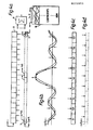
- a QPSK (quad phase shift key) signal comprises 4 symbols S1, S2, S3, S4 each of which is represented by a particular phase of a phase modulated carrier signal.
- the symbols fall within respective quadrants of the phase vector diagram illustrated in Figure 1.
- the four symbols S3, S2, S4, S1 represent respective values (Real, 1m; D2,D1) -1-1, -11, 1-1, 11 the pairs of values identifying the quadrants as shown in Figure 1.
- a carrier is phase modulated with the symbols S1-S4 each symbol occupying a number e.g. one of cycles of the carrier.
- Figure 2 shows abrupt phase transitions between symbols, in fact phase transitions between symbols in the phase modulated signal are not abrupt but follow phase change trajectories. One such trajectory is shown in dotted lines in Figure 1.
- an RF signal of e.g. 70MHz carrier frequency which is QPSK phase modulated is provided to a mixer where it is mixed with a local oscillator signal of e.g. 68 MHz and band-pass filtered to produce a signal of e.g. 2MBd symbol frequency on a carrier of 2MHz frequency.
- the RF signal itself may have been derived from a signal of even higher carrier frequency by a previous mixer (not shown) and band pass filter (now shown) as known in the art.
- the resulting (analogue) signal is then sampled and digitised in an analogue to digital converter 2 which is responsive to an 8 MHz sampling clock 3 which produces 4 samples per cycle of carrier. In the case of one symbol per cycle, that is also four samples per symbol.
- the clock is free running and so its phase is arbitrary and may vary relative to the incoming signal.
- the output of the converter 2 is a sequence of digital samples, each in 8 bit parallel form.
- the input to, and the output from the converter 2 is a real signal. Subsequent processing however takes place on a complex representation of the signal.
- the digital samples are multiplied in a converter 21 by two signals which convert the samples into their real and imaginary parts corresponding to (cos+jsin)
- the two signals are +1, 0, -1, 0, + 1 which corresponds to a cosine function and 0, +1, 0, -1, 0 which corresponds to a sine function.
- the two signals are in constant phase and frequency relation with the clock 3.
- the output of the converter 21 is in 16 bit (2x8 bit) parallel form where one set of 8 bits represents the real part and the other set represents the imaginary part.
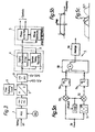
- the digital samples are fed to a digital "symbol timing recovery” (STR) circuit 4 which produces a signal indicative of symbol timing, which signal is fed forward to an interpolating filter 6.
- the timing recovery circuit 4 derives the timing information from the signal provided at the input to the filter 6.
- the timing information is fed-forward.
- the timing information could be derived by feed-back from e.g. the output of the STR circuit as shown in the dotted line 8 in Figure 3 or from the output of the phase recovery circuit, feed forward has the following advantages over feed-back:
- the interpolating filter 6 is a "Ny quist" filter having a variable phase slope controlled by the symbol timing recovery circuit.
- the interpolation filter together with the STR circuit 4 performs the following function:
- the result is the regeneration, in digital form, of the originally transmitted set of phase/amplitude states, but with an arbitrary rotation of the phase plane.
- FIG. 4a one possible version of a digital filter 6 in accordance with an aspect of the invention is shown.
- the shown filter is for processing the real parts. It is duplicated for processing the imaginary parts.
- the shown filter comprises an 18 stage shift register 8, each stage of which is 8 bits wide to accommodate 8 bit wide samples.
- Each stage of the register is coupled to an associated multiplier 9 which is also arranged to receive a coefficient from a read only memory 10 (the coefficients ROM) which stores many sets of coefficients.
- the coefficients ROM read only memory
- the outputs of the multipliers are summed in an adder 11 which produces samples corresponding to samples of substantially optimum timing.
- the filter convolves the digital signal which is clocked through the shift register 8 with a function represented by the coefficients supplied to the multipliers.
- the function represented by the coefficients is chosen to define the Nyquist filtering characteristic of the demodulator (taking into account other filters in the demodulator).
- the coefficients lie on the envelope of a typical impulse response.
- variable propagation delays occur and the timing of the signal in the shift register varies. Also the phase of the sampling clock of the A/D converter relative to the incoming signal is arbitrary.
- the cho ice of coefficients is determined by the output of the signal timing recovering circuit 4.
- the coefficients supplied to the multipliers C1-C36 are changed in accordance with the phase shift ⁇ which has a maximum value of +/- 1/2 the symbol timing.
- the phase shift is compensated for by, in effect, shifting the impulse function by a corresponding amount. That is done by supplying the multipliers with the coefficients which would lie on the shifted impulse response at the positions corresponding to the positions of the multipliers.
- Sets of the 18 coefficients are stored in the ROM 10.
- the set appropriate to any particular phase shift is chosen and read out of the ROM.
- the number of sets stored is a matter of choice.
- the ROM stores 256 x 9 samples of the impulse response arranged so that the required 2 x 9 coefficients can be selected by the output of the STR circuit acting as an address.
- the symbol stream at the input to the digital filter is also fed to an input 50 of the timing symbol recovery circuit 4.
- the symbol stream is then fed to a circuit 51 which outputs the complex conjugate of its input.
- the symbol stream is also fed to a mixer 52, and the complex conjugate is fed to another mixer 53.
- Both mixers also receive a clock signal of frequency equal to one half the symbol rate.
- the clock signal is derived from the free running clock 3 ( Figure 3) and has a constant phase and frequency relationship with it.
- the form of the clock signal is 1,j,-1,-j,1, etc.
- the outputs of the mixers are provided to two identical filters 54 which select and filter those components of the outputs of the mixers which fall within a common frequency band defined by the filters.
- the outputs of the filters are multiplied in a circuit 55 which determines the phase of the symbol stream, and an averager 56 averages the phase values over a predetermined number of symbol periods, to produce the signal indicating the symbol timing.
- the number of symbol periods over which averaging takes place is chosen to be long enough to ensure that the standard deviation of the phase estimate is reduced to the desired level.
- the form of the averager is as known in the art.
- FIG. 5b there is shown the signal frequency characteristic centred about zero frequency.
- the characteristic is flat except at its end zones which are for example raised-cosine shaped.
- the end zones are skew symmetric about Nyquist frequencies which are spaced from zero by half the symbol frequency.
- the frequency separation between the Nyquist frequencies in the end zones contain the desired information relating to symbol timing.
- the clock signal beats both the end zones to a range around zero frequency so that they both fall within the filter frequency response ⁇ (f) of the filter 54 which is also centred around zero frequency.
- the filter frequency response ⁇ (f) is chosen to pass the respective end zones and to reject adjacent channel interference (ACI) and out of band thermal noise and to reject response to the signals within the remainder of the channel characteristic which would otherwise contribute noise into the symbol time estimate, as beaten down by the clock.
- ACI adjacent channel interference
- the complex conjugate operation (51) in the lower arm causes frequency to be negated, so that the lower end zone becomes mapped to the upper end zone (with its sp ectrum complex conjugated), whence it is mapped to near zero frequency by the clock.
- the circuit 55 is a multiplier which determines the symbol timing phase with respect to the clock by multiplying the two end zones together in the time domain.
- the incoming real and imaginary parts at input 50 can be processed separately and the output of the filters 54 can be worked out for each part. Having determined the response of the top arm to the real part of the input and having also determined the response of the top arm to the imaginary part of the input, it follows that the output of the top arm filter 54 is the sum of the responses and the output of the bottom arm filter is the difference between the responses. That process is very efficient computatically.
- the output of each filter 54 is at symbol rate.
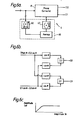
- the phase recovery circuit comprises a carrier phase estimating circuit 60 and a phase correcting circuit 61 responsive to circuit 60.
- the phase recovery circuit rotates the phase plane of the digital signal produced by the symbol timing correction circuit back to its original orientation to recover the transmitted data streams.
- the phase estimation circuit takes the symbol stream from the output of the digital filter 6 ( Figure 3) and estimates its phase, the phase estimate being fed forward to the phase corrector.
- the phase estimator 60 comprises a circuit 62 which determines the fourth power of the symbol stream, but with soft limiting (as shown in Figure 6c) of the resultant amplitude of the output signal, a technique known in the art.
- the output of the circuit 62 is averaged over a chosen number of symbol periods to produce a measure of the phase which is then reduced in circuit 63 by the power 1/4. That measure is used in known manner as shown in Figure 6b to produce the correct symbol values D1, D2 (see Figure 1).
- the circuits 61 and 63 are preferably ROMs which are addressed by the symbol stream at their inputs so as to read out the corresponding output values.
- phase recovery circuit operates on a digital sampled signal the sampling points of which have been optimised it operates more effectively because it does not then respond to the pattern dependent phase trajectories across the phase plane.
- the digital filter 6 for example may not comprise a shift register 8; instead the digitised samples may be written into memory locations.
- the multipliers 9 and added 11 may be implemented by an arithmetic logic unit and accumulator of a computing device which accesses the memory locations and the ROM 10.
- phase modulation schemes involving more or less than four phases e.g. BPSK (bi phase shift key). It is also applicable to signals which are phase and amplitude modulated or to signals which are amplitude modulated. It is, for example, applicable to a QAM (quadrature amplitude modulated) signal or a PAM (pulse amplitude modulated) signal.
- BPSK bi phase shift key
- Figures 5a to 5c describe a preferred novel form of STR circuit
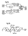
- Figures 7a to b another form of an STR circuit is shown in Figures 7a to b.
- a desirable feature of a STR circuit is that it presents equal and optimal sensitivity through the whole of 360 degrees.
- a known STR circuit using the maximum likelihood technique does not provide that feature.
- Figure 7 discloses a novel symbol-timing-phase-detector with Maximum-Likelihood properties and equal sensitivity for all symbol-timing phase errors.
- This estimator is a quadrature version of the conventional Maximum-Likelihood symbol-timing-phase estimator. This has the property that at acquisition there is no possibility of hang-up (because the quadrature arm forces the STR system off the metastable point).
Landscapes
- Engineering & Computer Science (AREA)
- Computer Networks & Wireless Communication (AREA)
- Signal Processing (AREA)
- Digital Transmission Methods That Use Modulated Carrier Waves (AREA)
Applications Claiming Priority (2)
| Application Number | Priority Date | Filing Date | Title |
|---|---|---|---|
| GB8527248 | 1985-11-05 | ||
| GB8527248 | 1985-11-05 |
Publications (3)
| Publication Number | Publication Date |
|---|---|
| EP0222593A2 true EP0222593A2 (de) | 1987-05-20 |
| EP0222593A3 EP0222593A3 (en) | 1988-03-30 |
| EP0222593B1 EP0222593B1 (de) | 1991-06-26 |
Family
ID=10587751
Family Applications (1)
| Application Number | Title | Priority Date | Filing Date |
|---|---|---|---|
| EP86308627A Expired EP0222593B1 (de) | 1985-11-05 | 1986-11-05 | Digitale Filter und Demodulatoren |
Country Status (3)
| Country | Link |
|---|---|
| US (1) | US4794341A (de) |
| EP (1) | EP0222593B1 (de) |
| DE (1) | DE3679960D1 (de) |
Cited By (9)
| Publication number | Priority date | Publication date | Assignee | Title |
|---|---|---|---|---|
| JPH02101845A (ja) * | 1988-08-15 | 1990-04-13 | Northern Telecom Ltd | Tdma信号搬送波再生システム |
| EP0413153A3 (en) * | 1989-07-17 | 1992-03-18 | Nec Corporation | Quadrature phase demodulation using a training sequence and a local signal offset from the received carrier frequency |
| EP0402742A3 (de) * | 1989-06-05 | 1992-09-02 | Victor Company Of Japan, Limited | Rauschformungsrequantisierungsschaltkreis |
| EP0498022A3 (en) * | 1991-01-28 | 1992-11-04 | Industrial Technology Research Institute | Timing recovery method and system for a receiver with a/d conversion |
| EP0573696A1 (de) * | 1992-06-05 | 1993-12-15 | Industrial Technology Research Institute | Taktwiedergewinnungsverfahren und -system |
| EP0601605A3 (en) * | 1992-12-11 | 1995-08-23 | Mitsubishi Electric Corp | Clock recovery circuit of a demodulator. |
| US5500874A (en) * | 1993-01-28 | 1996-03-19 | Signal Processors Limited | Digital filtering, data rate conversion and modem design |
| EP0763919A3 (de) * | 1995-09-18 | 2000-08-09 | Mitsubishi Denki Kabushiki Kaisha | QPSK-Demodulator mit Frequenz- und Phasennachlauf |
| EP0871305A3 (de) * | 1997-02-12 | 2002-08-21 | Fujitsu Limited | Anordnung und Verfahren zur Zeitphasenregelung |
Families Citing this family (17)
| Publication number | Priority date | Publication date | Assignee | Title |
|---|---|---|---|---|
| JP2613256B2 (ja) * | 1988-05-25 | 1997-05-21 | 株式会社日立製作所 | ディジタル復調装置 |
| US5073907A (en) * | 1990-01-30 | 1991-12-17 | California Institute Of Technology | Digital phase-lock loop |
| US5121072A (en) * | 1990-11-27 | 1992-06-09 | Rockwell International Corporation | Digital demodulator for amplitude or angle modulation using truncated nonlinear power series approximations |
| JP3255179B2 (ja) * | 1992-02-14 | 2002-02-12 | ソニー株式会社 | データ検出装置 |
| US5263054A (en) * | 1992-05-21 | 1993-11-16 | International Business Machines Corporation | Method and system for interpolating baud rate timing recovery for asynchronous start stop protocol |
| DE4237692C1 (de) * | 1992-11-07 | 1994-03-03 | Grundig Emv | Empfänger für ein digitales Rundfunksignal |
| JP3693301B2 (ja) * | 1993-05-07 | 2005-09-07 | コーニンクレッカ フィリップス エレクトロニクス エヌ ヴィ | 改善されたタイミング手段を有する受信機からなる送信方式 |
| US5602883A (en) * | 1993-10-13 | 1997-02-11 | The United States Of America As Represented By The Administrator Of The National Aeronautics And Space Administration | Method of implementing digital phase-locked loops |
| US5684835A (en) * | 1994-10-13 | 1997-11-04 | Westinghouse Electric Corporation | Locally coherent QPSK detection with differential decoding for a fading channel |
| US5748680A (en) * | 1994-12-16 | 1998-05-05 | Lucent Technologies Inc. | Coarse frequency burst detector for a wireline communications system |
| US5592176A (en) * | 1995-03-30 | 1997-01-07 | Scientific-Atlanta, Inc. | Tracking system for tracking a moving signal source |
| US5640416A (en) * | 1995-06-07 | 1997-06-17 | Comsat Corporation | Digital downconverter/despreader for direct sequence spread spectrum communications system |
| ES2113301B1 (es) * | 1995-10-27 | 1999-01-01 | Alcatel Espacio Sa | Dispositivo de interpolacion de señales. |
| US6128357A (en) * | 1997-12-24 | 2000-10-03 | Mitsubishi Electric Information Technology Center America, Inc (Ita) | Data receiver having variable rate symbol timing recovery with non-synchronized sampling |
| KR100324749B1 (ko) * | 1998-10-09 | 2002-03-13 | 구자홍 | 최대 가능성 심볼 타이밍 복원기 |
| EP1632052A1 (de) * | 2003-05-27 | 2006-03-08 | Koninklijke Philips Electronics N.V. | Phasennachführung für empfangssignale mittels adaptiver interpolation |
| GB0609601D0 (en) * | 2006-05-15 | 2006-06-21 | Ttp Communications Ltd | Timing errors |
Citations (1)
| Publication number | Priority date | Publication date | Assignee | Title |
|---|---|---|---|---|
| EP0092400A2 (de) | 1982-04-20 | 1983-10-26 | Trw Inc. | Digitales Synchronisationsverfahren |
Family Cites Families (8)
| Publication number | Priority date | Publication date | Assignee | Title |
|---|---|---|---|---|
| GB1523641A (en) * | 1976-04-29 | 1978-09-06 | Plessey Co Ltd | Adaptive equalisers for phase modulation data transmission systems |
| GB1533773A (en) * | 1977-02-07 | 1978-11-29 | Plessey Co Ltd | Frame synchronisation arrangements for use in data transmission systems |
| WO1984001874A1 (en) * | 1982-10-29 | 1984-05-10 | Devon County Council | Signal encoding-decoding apparatus |
| JPS59161149A (ja) * | 1983-03-04 | 1984-09-11 | Nec Corp | タイミング同期回路 |
| WO1986000185A1 (en) * | 1984-06-09 | 1986-01-03 | Devon County Council | Data communication method and appartus |
| JPS6156555A (ja) * | 1984-08-27 | 1986-03-22 | Nec Corp | 復調装置 |
| EP0204745B2 (de) * | 1984-11-22 | 1995-09-06 | Devon County Council | Daten-modulator-demodulatorsystem |
| GB8507903D0 (en) * | 1985-03-26 | 1985-05-01 | Tomlinson M | Noise-reduction signal processing arrangement |
-
1986
- 1986-11-04 US US06/926,529 patent/US4794341A/en not_active Expired - Fee Related
- 1986-11-05 DE DE8686308627T patent/DE3679960D1/de not_active Expired - Lifetime
- 1986-11-05 EP EP86308627A patent/EP0222593B1/de not_active Expired
Patent Citations (1)
| Publication number | Priority date | Publication date | Assignee | Title |
|---|---|---|---|---|
| EP0092400A2 (de) | 1982-04-20 | 1983-10-26 | Trw Inc. | Digitales Synchronisationsverfahren |
Non-Patent Citations (1)
| Title |
|---|
| MUELER; MUELER: "Adaptive Timing Recovery in Digital Synchronis Data Receivers", INTERNATIONAL ZURICH SEMINAR ON DIGITAL COMMUNICATIONS, 12 March 1974 (1974-03-12) |
Cited By (15)
| Publication number | Priority date | Publication date | Assignee | Title |
|---|---|---|---|---|
| JPH02101845A (ja) * | 1988-08-15 | 1990-04-13 | Northern Telecom Ltd | Tdma信号搬送波再生システム |
| EP0355587A3 (de) * | 1988-08-15 | 1991-11-27 | Nortel Networks Corporation | Takt- und Trägerrückgewinnung für TDMA ohne Präambelfolge |
| EP0402742A3 (de) * | 1989-06-05 | 1992-09-02 | Victor Company Of Japan, Limited | Rauschformungsrequantisierungsschaltkreis |
| EP0413153A3 (en) * | 1989-07-17 | 1992-03-18 | Nec Corporation | Quadrature phase demodulation using a training sequence and a local signal offset from the received carrier frequency |
| US5404379A (en) * | 1991-01-28 | 1995-04-04 | Industrial Technology Research Institute | Timing recovery method and system |
| EP0498022A3 (en) * | 1991-01-28 | 1992-11-04 | Industrial Technology Research Institute | Timing recovery method and system for a receiver with a/d conversion |
| EP0573696A1 (de) * | 1992-06-05 | 1993-12-15 | Industrial Technology Research Institute | Taktwiedergewinnungsverfahren und -system |
| EP0601605A3 (en) * | 1992-12-11 | 1995-08-23 | Mitsubishi Electric Corp | Clock recovery circuit of a demodulator. |
| US5541958A (en) * | 1992-12-11 | 1996-07-30 | Mitsubishi Denki Kabushiki Kaisha | Clock recovery circuit of demodulator |
| US5640426A (en) * | 1992-12-11 | 1997-06-17 | Mitsubishi Denki Kabushiki Kaisha | Clock recovery circuit of demodulator |
| US5651031A (en) * | 1992-12-11 | 1997-07-22 | Mitsubishi Denki Kabushiki Kaisha | Clock recovery circuit of demodulator |
| EP0978972A3 (de) * | 1992-12-11 | 2000-03-29 | Mitsubishi Denki Kabushiki Kaisha | Taktrückgewinnung für einen Demodulator |
| US5500874A (en) * | 1993-01-28 | 1996-03-19 | Signal Processors Limited | Digital filtering, data rate conversion and modem design |
| EP0763919A3 (de) * | 1995-09-18 | 2000-08-09 | Mitsubishi Denki Kabushiki Kaisha | QPSK-Demodulator mit Frequenz- und Phasennachlauf |
| EP0871305A3 (de) * | 1997-02-12 | 2002-08-21 | Fujitsu Limited | Anordnung und Verfahren zur Zeitphasenregelung |
Also Published As
| Publication number | Publication date |
|---|---|
| EP0222593B1 (de) | 1991-06-26 |
| US4794341A (en) | 1988-12-27 |
| DE3679960D1 (de) | 1991-08-01 |
| EP0222593A3 (en) | 1988-03-30 |
Similar Documents
| Publication | Publication Date | Title |
|---|---|---|
| EP0222593B1 (de) | Digitale Filter und Demodulatoren | |
| JP2526931B2 (ja) | Psk信号復調装置 | |
| US4583048A (en) | MSK digital demodulator for burst communications | |
| CA2170344C (en) | Signal processing system | |
| US5255290A (en) | Method and apparatus for combined frequency offset and timing offset estimation | |
| EP0375272B1 (de) | Kohärenter Demodulator für phasenumgetastete Signale | |
| US5602835A (en) | OFDM synchronization demodulation circuit | |
| US5588027A (en) | Digital demodulating method and circuit for use in a time-division multiple access channel | |
| JP4366808B2 (ja) | タイミングエラー検出回路および復調回路とその方法 | |
| JP3728573B2 (ja) | 復調装置 | |
| US4344176A (en) | Time recovery circuitry in a modem receiver | |
| JP3575883B2 (ja) | ディジタル復調器 | |
| EP0486839B1 (de) | Quasi-kohärenter MPSK-Demodulator | |
| US5867059A (en) | Demodulating system for MSK and GMSK signal using a fast fourier transform converter | |
| CA1277723C (en) | Digital filters and demodulators | |
| US5832045A (en) | Method and apparatus for recovering baud timing from correlation of intersymbol interference | |
| JP2931454B2 (ja) | ディジタル位相変調信号復調回路 | |
| US5838736A (en) | Method and apparatus for generating carriers for phase demodulation having at least two phase states, and a corresponding demodulation stage | |
| KR100433639B1 (ko) | 잔류측파대변조시타이밍회복을위한장치및방법 | |
| US7263139B1 (en) | Phase correction for a phase modulated signal with mutually interfering symbols | |
| JPH07235956A (ja) | バースト信号復調回路 | |
| JPH0870332A (ja) | クロック再生装置 | |
| US8175202B2 (en) | Receiver with clock drift compensation | |
| JP2958612B2 (ja) | 多値qam復調装置 | |
| JP2000183992A (ja) | クロック再生方法および回路 |
Legal Events
| Date | Code | Title | Description |
|---|---|---|---|
| PUAI | Public reference made under article 153(3) epc to a published international application that has entered the european phase |
Free format text: ORIGINAL CODE: 0009012 |
|
| AK | Designated contracting states |
Kind code of ref document: A2 Designated state(s): DE FR GB IT |
|
| PUAL | Search report despatched |
Free format text: ORIGINAL CODE: 0009013 |
|
| AK | Designated contracting states |
Kind code of ref document: A3 Designated state(s): DE FR GB IT |
|
| 17P | Request for examination filed |
Effective date: 19880919 |
|
| 17Q | First examination report despatched |
Effective date: 19890706 |
|
| GRAA | (expected) grant |
Free format text: ORIGINAL CODE: 0009210 |
|
| AK | Designated contracting states |
Kind code of ref document: B1 Designated state(s): DE FR GB IT |
|
| REF | Corresponds to: |
Ref document number: 3679960 Country of ref document: DE Date of ref document: 19910801 |
|
| ET | Fr: translation filed | ||
| ITF | It: translation for a ep patent filed | ||
| PLBE | No opposition filed within time limit |
Free format text: ORIGINAL CODE: 0009261 |
|
| STAA | Information on the status of an ep patent application or granted ep patent |
Free format text: STATUS: NO OPPOSITION FILED WITHIN TIME LIMIT |
|
| 26N | No opposition filed | ||
| PGFP | Annual fee paid to national office [announced via postgrant information from national office to epo] |
Ref country code: GB Payment date: 19981105 Year of fee payment: 13 |
|
| PGFP | Annual fee paid to national office [announced via postgrant information from national office to epo] |
Ref country code: FR Payment date: 19981130 Year of fee payment: 13 |
|
| PGFP | Annual fee paid to national office [announced via postgrant information from national office to epo] |
Ref country code: DE Payment date: 19990125 Year of fee payment: 13 |
|
| PG25 | Lapsed in a contracting state [announced via postgrant information from national office to epo] |
Ref country code: GB Free format text: LAPSE BECAUSE OF NON-PAYMENT OF DUE FEES Effective date: 19991105 |
|
| GBPC | Gb: european patent ceased through non-payment of renewal fee |
Effective date: 19991105 |
|
| PG25 | Lapsed in a contracting state [announced via postgrant information from national office to epo] |
Ref country code: FR Free format text: LAPSE BECAUSE OF NON-PAYMENT OF DUE FEES Effective date: 20000731 |
|
| PG25 | Lapsed in a contracting state [announced via postgrant information from national office to epo] |
Ref country code: DE Free format text: LAPSE BECAUSE OF NON-PAYMENT OF DUE FEES Effective date: 20000901 |
|
| REG | Reference to a national code |
Ref country code: FR Ref legal event code: ST |
|
| PG25 | Lapsed in a contracting state [announced via postgrant information from national office to epo] |
Ref country code: IT Free format text: LAPSE BECAUSE OF NON-PAYMENT OF DUE FEES;WARNING: LAPSES OF ITALIAN PATENTS WITH EFFECTIVE DATE BEFORE 2007 MAY HAVE OCCURRED AT ANY TIME BEFORE 2007. THE CORRECT EFFECTIVE DATE MAY BE DIFFERENT FROM THE ONE RECORDED. Effective date: 20051105 |