EP0223969A1 - Connecteur avec un contact à faible force d'insertion - Google Patents
Connecteur avec un contact à faible force d'insertion Download PDFInfo
- Publication number
- EP0223969A1 EP0223969A1 EP86113319A EP86113319A EP0223969A1 EP 0223969 A1 EP0223969 A1 EP 0223969A1 EP 86113319 A EP86113319 A EP 86113319A EP 86113319 A EP86113319 A EP 86113319A EP 0223969 A1 EP0223969 A1 EP 0223969A1
- Authority
- EP
- European Patent Office
- Prior art keywords
- contact
- connector block
- daughter board
- engaging
- Prior art date
- Legal status (The legal status is an assumption and is not a legal conclusion. Google has not performed a legal analysis and makes no representation as to the accuracy of the status listed.)
- Withdrawn
Links
- 238000003780 insertion Methods 0.000 title claims abstract description 21
- 230000037431 insertion Effects 0.000 title claims abstract description 21
- 230000009977 dual effect Effects 0.000 claims abstract description 9
- 238000005476 soldering Methods 0.000 claims description 13
- 229910000881 Cu alloy Inorganic materials 0.000 claims description 6
- 238000010276 construction Methods 0.000 abstract description 7
- 230000013011 mating Effects 0.000 abstract description 2
- 239000000463 material Substances 0.000 description 4
- 229910001369 Brass Inorganic materials 0.000 description 2
- 238000005452 bending Methods 0.000 description 2
- 239000010951 brass Substances 0.000 description 2
- 239000004033 plastic Substances 0.000 description 2
- 229920003023 plastic Polymers 0.000 description 2
- 230000000717 retained effect Effects 0.000 description 2
- 229910000906 Bronze Inorganic materials 0.000 description 1
- OAICVXFJPJFONN-UHFFFAOYSA-N Phosphorus Chemical compound [P] OAICVXFJPJFONN-UHFFFAOYSA-N 0.000 description 1
- ATJFFYVFTNAWJD-UHFFFAOYSA-N Tin Chemical compound [Sn] ATJFFYVFTNAWJD-UHFFFAOYSA-N 0.000 description 1
- 229910045601 alloy Inorganic materials 0.000 description 1
- 239000000956 alloy Substances 0.000 description 1
- 239000010974 bronze Substances 0.000 description 1
- KUNSUQLRTQLHQQ-UHFFFAOYSA-N copper tin Chemical compound [Cu].[Sn] KUNSUQLRTQLHQQ-UHFFFAOYSA-N 0.000 description 1
- 238000005516 engineering process Methods 0.000 description 1
- 238000012423 maintenance Methods 0.000 description 1
- 230000014759 maintenance of location Effects 0.000 description 1
- 239000002184 metal Substances 0.000 description 1
- 229910052751 metal Inorganic materials 0.000 description 1
- 239000012778 molding material Substances 0.000 description 1
- 238000000465 moulding Methods 0.000 description 1
- 229910000679 solder Inorganic materials 0.000 description 1
Images


Classifications
-
- H—ELECTRICITY
- H01—ELECTRIC ELEMENTS
- H01R—ELECTRICALLY-CONDUCTIVE CONNECTIONS; STRUCTURAL ASSOCIATIONS OF A PLURALITY OF MUTUALLY-INSULATED ELECTRICAL CONNECTING ELEMENTS; COUPLING DEVICES; CURRENT COLLECTORS
- H01R13/00—Details of coupling devices of the kinds covered by groups H01R12/70 or H01R24/00 - H01R33/00
- H01R13/02—Contact members
- H01R13/10—Sockets for co-operation with pins or blades
- H01R13/11—Resilient sockets
- H01R13/115—U-shaped sockets having inwardly bent legs, e.g. spade type
-
- H—ELECTRICITY
- H01—ELECTRIC ELEMENTS
- H01R—ELECTRICALLY-CONDUCTIVE CONNECTIONS; STRUCTURAL ASSOCIATIONS OF A PLURALITY OF MUTUALLY-INSULATED ELECTRICAL CONNECTING ELEMENTS; COUPLING DEVICES; CURRENT COLLECTORS
- H01R12/00—Structural associations of a plurality of mutually-insulated electrical connecting elements, specially adapted for printed circuits, e.g. printed circuit boards [PCB], flat or ribbon cables, or like generally planar structures, e.g. terminal strips, terminal blocks; Coupling devices specially adapted for printed circuits, flat or ribbon cables, or like generally planar structures; Terminals specially adapted for contact with, or insertion into, printed circuits, flat or ribbon cables, or like generally planar structures
- H01R12/70—Coupling devices
- H01R12/82—Coupling devices connected with low or zero insertion force
-
- H—ELECTRICITY
- H01—ELECTRIC ELEMENTS
- H01R—ELECTRICALLY-CONDUCTIVE CONNECTIONS; STRUCTURAL ASSOCIATIONS OF A PLURALITY OF MUTUALLY-INSULATED ELECTRICAL CONNECTING ELEMENTS; COUPLING DEVICES; CURRENT COLLECTORS
- H01R12/00—Structural associations of a plurality of mutually-insulated electrical connecting elements, specially adapted for printed circuits, e.g. printed circuit boards [PCB], flat or ribbon cables, or like generally planar structures, e.g. terminal strips, terminal blocks; Coupling devices specially adapted for printed circuits, flat or ribbon cables, or like generally planar structures; Terminals specially adapted for contact with, or insertion into, printed circuits, flat or ribbon cables, or like generally planar structures
- H01R12/70—Coupling devices
- H01R12/71—Coupling devices for rigid printing circuits or like structures
- H01R12/72—Coupling devices for rigid printing circuits or like structures coupling with the edge of the rigid printed circuits or like structures
- H01R12/722—Coupling devices for rigid printing circuits or like structures coupling with the edge of the rigid printed circuits or like structures coupling devices mounted on the edge of the printed circuits
- H01R12/724—Coupling devices for rigid printing circuits or like structures coupling with the edge of the rigid printed circuits or like structures coupling devices mounted on the edge of the printed circuits containing contact members forming a right angle
-
- H—ELECTRICITY
- H01—ELECTRIC ELEMENTS
- H01R—ELECTRICALLY-CONDUCTIVE CONNECTIONS; STRUCTURAL ASSOCIATIONS OF A PLURALITY OF MUTUALLY-INSULATED ELECTRICAL CONNECTING ELEMENTS; COUPLING DEVICES; CURRENT COLLECTORS
- H01R13/00—Details of coupling devices of the kinds covered by groups H01R12/70 or H01R24/00 - H01R33/00
- H01R13/40—Securing contact members in or to a base or case; Insulating of contact members
- H01R13/42—Securing in a demountable manner
- H01R13/428—Securing in a demountable manner by resilient locking means on the contact members; by locking means on resilient contact members
- H01R13/432—Securing in a demountable manner by resilient locking means on the contact members; by locking means on resilient contact members by stamped-out resilient tongue snapping behind shoulder in base or case
Definitions
- This invention relates to a low insertion force contact, used in a low engaging force interconnection system consisting of a daughter board and a mother board.
- the electrical connection is established by means of mating pins of the connector on the mother board connecting to the low insertion force contacts of the connector block on the daughter board.
- the electrical connection between mother board and daughter board is achieved by engaging the pin contacts of the mother board connector with the low insertion force contacts of the daughter board connector block.
- mother/daughter board type connectors and contacts are generally discussed in U.S. Patent 4,439,000 and in the references cited on the face thereof.
- card edge connectors for example, a single row with a maximum of about 50 contacts.
- high density interconnecting connectors i.e., those with up to about 800 contacts, were developed, and which required a low insertion force contact.
- Such contacts are generally of complicated construction to ensure retention within a daughter board connecting block.
- such contacts are inserted into the daughter board connector block from the front thereof.
- Contact is then established by insertion of a pin contact extending from the mother board into receiving pockets, i.e., passages extending throughout the connector block, holding respective low insertion force contacts.
- the contacts are dimensioned so that they cannot be passed out from the pocket through the other or near side of the block.
- Still another object is to provide such a contact which allows molding of the connector block with which it is employed to be conducted in a simple manner without requiring maintenance of precise tolerances.
- Yet still another object of the present invention is to provide such a contact which ensures good electrical connection with connecting pin contacts extending from a mother board to which it is connected, and which is structured for being reliably retained within the connector block with which it is employed.
- a contact comprising a substantially channel type longitudinally projecting body construction.
- the body includes a termination end at one end thereof which is constructed for being bent over at an angle approximately perpendicular to the body for insertion and connection by soldering to a daughter board.
- Spring contact engagement means is located at the other end of the body for engaging a pin contact from a mother board with a predetermined force when the contact is received in a connector block of the daughter board.
- retaining means for engaging a wall of pockets of the daughter board connector block, after the contact has been inserted therein, for resisting removal therefrom when the contact is received in a passage of the connector block prior to fixed attachment of the connector block to the daughter board along with soldering of the termination end of the contact to the daughter board.
- the spring contact engagment means comprises dual in-line tines or beams which have been punched out from the body and bent or constructed in a manner such that they are spaced from the walls of a pocket in the connector block by a predetermined distance less than the size of a pin contact with which it is to establish electrical connection in the pocket of the connector block with a predetermined force when received therein.
- a pin contact for example, from a mother board is inserted into the connector block pocket, from the front of the connector block, it is held with a predetermined force by the dual in-line beams, between the dual in-line beams and a wall of the pocket.
- the retaining means preferably comprises a punched out flexible tab which bends when the contact is inserted into a receiving passage from the top of the connector block, and once received therein, resists removal prior to soldering to the daughter board, in the same direction of insertion by engaging the walls of the passage with the end of the tab.
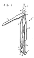
- the contact l is generally elongated in shape and of typically a U-shaped construction having a channel 3 extending the length thereof.
- a first terminating end 5 is provided for being inserted into a through hole of a daughter board for soldering therein to establish electrical connection therewith.
- the remaining portion of the contact is constructed for being received within a daughter board connector block which is typically firmly attached to a daughter board, i.e. a printed circuit board constructed for being connected a mother board, i.e. another printed circuit board of the type which includes various daughter boards connected thereto.
- the construction of the contact l is such as to be readily inserted into pockets of a connector block 25 in a manner such that the termination end 5 can be bent at a point 7 at an angle of appoximately 90° with respect to the remainder of the body of the contact l.
- the contact l For insertion into the connector block, the contact l includes a compressible punched out tab l9 which permits entry into pockets in a connector block from the rear thereof whereby the tab l9 is compressed and prior to soldering of the end 5 to a daughter board and secure attachment of the connector block thereto, serves to restrain the contact l from being withdrawn from the connector block by engaging the walls of the pocket wherein it is received.
- the contact l also includes dual in-line beams or tines ll and l3 which serve to compressively engage a pin contact 23 of the mother board as will be discussed in greater detail hereinafter.
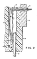
- the contact l in accordance with the invention is received within a pocket 29 of a daughter board 27 connector block 25. Once received in the pocket 29, the end 5 is bent over at point 7 and inserted within a through hole of a daughter board 27. It is held therein by soldering as shown at soldered region 3l. Prior to soldering, the tab l9 serves to prevent the contact l from being withdrawn from the rear portion of the pocket 29 after insertion. A projection 9 at the other end of the contact cooperates with a positioning ridge 2l within the pocket 29 to more accurately position the contact l within the pocket 29.
- Dual in-line beams or tines ll and l3 include respective engaging surfaces l5 and l7 ( Figure l) which in relaxed position are spaced by a predetermined distance smaller than the dimension of a pin contact 23 from the opposite wall of the pocket 29.
- the connector block 25 For connection to a mother board, the connector block 25 is brought down at the respective pocket 29 thereof to receive pin contacts 23 from a mother board which in turn compress the tines ll and l3 inwardly to establish electrical contact therewith. It is noted that tine ll cooperates with tine l3 by having a portion passing through an opening l3A of tine l3.
- the connector l includes a generally U-shaped channel 3 which aids in establishing the soldered connection to the daughter board 27.
- the assembly is generally inserted into a connector block 25 in the direction C as generally shown in Figure 7 with all contacts l being inserted at the same time and then the bending from the dotted line position of portion or end 5 at point 7 is then effected to permit insertion of the respective ends 5 into the respective through-holes of a daughter board.
- the entire assembly is more clearly shown received in the cross-sectional view of the daughter board connector block 25 shown in Figure 8.
- the connector block 25 itself, it is noted, as previously discussed, that it includes a molded-in ridge or rib 2l which is for the purpose of more precisely positioning the contact within the pocket 29 of the connector block 25.
- the connector block 25 will be manufactured of conventional plastics molding materials.
- the contact l itself, it must be made of a material which is sufficiently electrically conductive but wear resistant and resilient enough to establish electrical connection with a pin contact 23 of a mother board.
- the preferred materials are of a variety of copper alloys including phosphor bronze, tin brass and brass alloys of the type which are well known to those of ordinary skill in the art.
- the connector block 25 Although it was noted that plastics materials are preferred, any insulative type material will suffice.
- the connector block itself must be molded within precise tolerances so as to permit ease of entry of the contact of the invention and the matting pin in a cooperative manner.
- the channel or pocket must be sufficiently large from the rear portion so as to permit entry of the contact but sufficiently small at the front or bottom opening thereof to prevent passage of the contact therethrough while at the same time permitting passage of a pin contact from the mother board thereinto.
- the contact of the invention lends itself readily to automated assembly since insertion into the connector block 25 is from the rear. Accordingly, both insertion as well as bending and then soldering can be conducted in a simply sequential step operation by automated machinery as will be readily apparent to those of ordinary skill in the art.
Landscapes
- Coupling Device And Connection With Printed Circuit (AREA)
- Vending Machines For Individual Products (AREA)
Applications Claiming Priority (2)
| Application Number | Priority Date | Filing Date | Title |
|---|---|---|---|
| US79877485A | 1985-11-18 | 1985-11-18 | |
| US798774 | 1985-11-18 |
Publications (1)
| Publication Number | Publication Date |
|---|---|
| EP0223969A1 true EP0223969A1 (fr) | 1987-06-03 |
Family
ID=25174234
Family Applications (1)
| Application Number | Title | Priority Date | Filing Date |
|---|---|---|---|
| EP86113319A Withdrawn EP0223969A1 (fr) | 1985-11-18 | 1986-09-27 | Connecteur avec un contact à faible force d'insertion |
Country Status (2)
| Country | Link |
|---|---|
| EP (1) | EP0223969A1 (fr) |
| JP (1) | JPS62126573A (fr) |
Citations (3)
| Publication number | Priority date | Publication date | Assignee | Title |
|---|---|---|---|---|
| FR1308204A (fr) * | 1960-12-15 | 1962-11-03 | Amp Inc | Connecteurs électriques à douille |
| EP0015696A2 (fr) * | 1979-03-06 | 1980-09-17 | AMP INCORPORATED (a New Jersey corporation) | Borne électrique et connecteur en bordure pour circuit imprimé comprenant telles bornes |
| EP0147039A2 (fr) * | 1983-12-13 | 1985-07-03 | AMP INCORPORATED (a New Jersey corporation) | Connecteur monté sur une surface |
-
1986
- 1986-09-27 EP EP86113319A patent/EP0223969A1/fr not_active Withdrawn
- 1986-11-17 JP JP61272032A patent/JPS62126573A/ja active Pending
Patent Citations (3)
| Publication number | Priority date | Publication date | Assignee | Title |
|---|---|---|---|---|
| FR1308204A (fr) * | 1960-12-15 | 1962-11-03 | Amp Inc | Connecteurs électriques à douille |
| EP0015696A2 (fr) * | 1979-03-06 | 1980-09-17 | AMP INCORPORATED (a New Jersey corporation) | Borne électrique et connecteur en bordure pour circuit imprimé comprenant telles bornes |
| EP0147039A2 (fr) * | 1983-12-13 | 1985-07-03 | AMP INCORPORATED (a New Jersey corporation) | Connecteur monté sur une surface |
Also Published As
| Publication number | Publication date |
|---|---|
| JPS62126573A (ja) | 1987-06-08 |
Similar Documents
| Publication | Publication Date | Title |
|---|---|---|
| US4687267A (en) | Circuit board edge connector | |
| US5582519A (en) | Make-first-break-last ground connections | |
| US5112233A (en) | Electrical connector having contact retention means | |
| US5004434A (en) | Printed circuit board edge connector | |
| US5139446A (en) | Electrical connector assembly | |
| EP0806814A2 (fr) | Connecteur électrique ayant des moyens de rétention de contacts améliorés | |
| US4023879A (en) | Adjustable electrical connector with replaceable contact sub-assembly and variable strain relief | |
| EP0555963A1 (fr) | Connecteur avec bus de mise à la terre en une seule pièce | |
| EP0347097A1 (fr) | Système de connecteur électrique | |
| EP0569893A2 (fr) | Connecteur électrique à profil bas | |
| EP0543278A1 (fr) | Connecteur électrique à profile bas | |
| EP0232521A2 (fr) | Fiche à profil bas | |
| US5281165A (en) | Electrical connector shroud adapted for shorting bar removal | |
| EP0717468B1 (fr) | Connecteur interrompant d'abord les contacts polaires et après le contact à la terre | |
| EP0312240A2 (fr) | Pièce de connexion électrique femelle | |
| AU591635B2 (en) | Electrical connector | |
| EP0632549B1 (fr) | Ensemble connecteur électrique | |
| EP0497554B1 (fr) | Elément de fixation | |
| US4708416A (en) | Electrical connecting terminal for a connector | |
| EP0740372A2 (fr) | Connecteur électrique | |
| US5167544A (en) | Female electrical contact | |
| EP0546673A2 (fr) | Connecteur avec dispositif de rétention | |
| EP0654185B1 (fr) | Outil pour connecteur de combinaison | |
| US4494818A (en) | Mounting member for electrical contacts | |
| EP0223969A1 (fr) | Connecteur avec un contact à faible force d'insertion |
Legal Events
| Date | Code | Title | Description |
|---|---|---|---|
| PUAI | Public reference made under article 153(3) epc to a published international application that has entered the european phase |
Free format text: ORIGINAL CODE: 0009012 |
|
| AK | Designated contracting states |
Kind code of ref document: A1 Designated state(s): DE FR GB IT |
|
| 17P | Request for examination filed |
Effective date: 19871202 |
|
| RAP1 | Party data changed (applicant data changed or rights of an application transferred) |
Owner name: AMPHENOL CORPORATION |
|
| 17Q | First examination report despatched |
Effective date: 19900314 |
|
| STAA | Information on the status of an ep patent application or granted ep patent |
Free format text: STATUS: THE APPLICATION IS DEEMED TO BE WITHDRAWN |
|
| 18D | Application deemed to be withdrawn |
Effective date: 19910213 |
|
| RIN1 | Information on inventor provided before grant (corrected) |
Inventor name: PROVINSKY, JERRY |