EP0224091A1 - Halbleiteranordnung mit einem Schutztransistor - Google Patents
Halbleiteranordnung mit einem Schutztransistor Download PDFInfo
- Publication number
- EP0224091A1 EP0224091A1 EP86115431A EP86115431A EP0224091A1 EP 0224091 A1 EP0224091 A1 EP 0224091A1 EP 86115431 A EP86115431 A EP 86115431A EP 86115431 A EP86115431 A EP 86115431A EP 0224091 A1 EP0224091 A1 EP 0224091A1
- Authority
- EP
- European Patent Office
- Prior art keywords
- region
- semiconductor region
- type
- semiconductor
- diffusion
- Prior art date
- Legal status (The legal status is an assumption and is not a legal conclusion. Google has not performed a legal analysis and makes no representation as to the accuracy of the status listed.)
- Granted
Links
Images

Classifications
-
- H—ELECTRICITY
- H10—SEMICONDUCTOR DEVICES; ELECTRIC SOLID-STATE DEVICES NOT OTHERWISE PROVIDED FOR
- H10D—INORGANIC ELECTRIC SEMICONDUCTOR DEVICES
- H10D84/00—Integrated devices formed in or on semiconductor substrates that comprise only semiconducting layers, e.g. on Si wafers or on GaAs-on-Si wafers
- H10D84/40—Integrated devices formed in or on semiconductor substrates that comprise only semiconducting layers, e.g. on Si wafers or on GaAs-on-Si wafers characterised by the integration of at least one component covered by groups H10D12/00 or H10D30/00 with at least one component covered by groups H10D10/00 or H10D18/00, e.g. integration of IGFETs with BJTs
- H10D84/401—Combinations of FETs or IGBTs with BJTs
-
- H—ELECTRICITY
- H10—SEMICONDUCTOR DEVICES; ELECTRIC SOLID-STATE DEVICES NOT OTHERWISE PROVIDED FOR
- H10D—INORGANIC ELECTRIC SEMICONDUCTOR DEVICES
- H10D18/00—Thyristors
- H10D18/80—Bidirectional devices, e.g. triacs
-
- H—ELECTRICITY
- H10—SEMICONDUCTOR DEVICES; ELECTRIC SOLID-STATE DEVICES NOT OTHERWISE PROVIDED FOR
- H10D—INORGANIC ELECTRIC SEMICONDUCTOR DEVICES
- H10D62/00—Semiconductor bodies, or regions thereof, of devices having potential barriers
- H10D62/10—Shapes, relative sizes or dispositions of the regions of the semiconductor bodies; Shapes of the semiconductor bodies
- H10D62/124—Shapes, relative sizes or dispositions of the regions of semiconductor bodies or of junctions between the regions
- H10D62/125—Shapes of junctions between the regions
-
- H—ELECTRICITY
- H10—SEMICONDUCTOR DEVICES; ELECTRIC SOLID-STATE DEVICES NOT OTHERWISE PROVIDED FOR
- H10D—INORGANIC ELECTRIC SEMICONDUCTOR DEVICES
- H10D84/00—Integrated devices formed in or on semiconductor substrates that comprise only semiconducting layers, e.g. on Si wafers or on GaAs-on-Si wafers
- H10D84/101—Integrated devices comprising main components and built-in components, e.g. IGBT having built-in freewheel diode
- H10D84/131—Thyristors having built-in components
- H10D84/138—Thyristors having built-in components the built-in components being FETs
-
- H—ELECTRICITY
- H10—SEMICONDUCTOR DEVICES; ELECTRIC SOLID-STATE DEVICES NOT OTHERWISE PROVIDED FOR
- H10D—INORGANIC ELECTRIC SEMICONDUCTOR DEVICES
- H10D84/00—Integrated devices formed in or on semiconductor substrates that comprise only semiconducting layers, e.g. on Si wafers or on GaAs-on-Si wafers
- H10D84/40—Integrated devices formed in or on semiconductor substrates that comprise only semiconducting layers, e.g. on Si wafers or on GaAs-on-Si wafers characterised by the integration of at least one component covered by groups H10D12/00 or H10D30/00 with at least one component covered by groups H10D10/00 or H10D18/00, e.g. integration of IGFETs with BJTs
-
- H—ELECTRICITY
- H10—SEMICONDUCTOR DEVICES; ELECTRIC SOLID-STATE DEVICES NOT OTHERWISE PROVIDED FOR
- H10D—INORGANIC ELECTRIC SEMICONDUCTOR DEVICES
- H10D89/00—Aspects of integrated devices not covered by groups H10D84/00 - H10D88/00
- H10D89/60—Integrated devices comprising arrangements for electrical or thermal protection, e.g. protection circuits against electrostatic discharge [ESD]
- H10D89/601—Integrated devices comprising arrangements for electrical or thermal protection, e.g. protection circuits against electrostatic discharge [ESD] for devices having insulated gate electrodes, e.g. for IGFETs or IGBTs
- H10D89/811—Integrated devices comprising arrangements for electrical or thermal protection, e.g. protection circuits against electrostatic discharge [ESD] for devices having insulated gate electrodes, e.g. for IGFETs or IGBTs using FETs as protective elements
-
- H—ELECTRICITY
- H10—SEMICONDUCTOR DEVICES; ELECTRIC SOLID-STATE DEVICES NOT OTHERWISE PROVIDED FOR
- H10F—INORGANIC SEMICONDUCTOR DEVICES SENSITIVE TO INFRARED RADIATION, LIGHT, ELECTROMAGNETIC RADIATION OF SHORTER WAVELENGTH OR CORPUSCULAR RADIATION
- H10F30/00—Individual radiation-sensitive semiconductor devices in which radiation controls the flow of current through the devices, e.g. photodetectors
- H10F30/20—Individual radiation-sensitive semiconductor devices in which radiation controls the flow of current through the devices, e.g. photodetectors the devices having potential barriers, e.g. phototransistors
- H10F30/21—Individual radiation-sensitive semiconductor devices in which radiation controls the flow of current through the devices, e.g. photodetectors the devices having potential barriers, e.g. phototransistors the devices being sensitive to infrared, visible or ultraviolet radiation
- H10F30/26—Individual radiation-sensitive semiconductor devices in which radiation controls the flow of current through the devices, e.g. photodetectors the devices having potential barriers, e.g. phototransistors the devices being sensitive to infrared, visible or ultraviolet radiation the devices having three or more potential barriers, e.g. photothyristors
- H10F30/263—Photothyristors
Definitions
- the present invention relates to a semiconductor device, such as a thyristor or a triac, including a protecting MOS transistor.
- a zero-cross photo thyristor or a zero-cross photo triac which is turned on only at a zero-cross time point at which an AC voltage applied between a cathode and an anode crosses a zero line or at a time point near the zero-cross time point, has been proposed.
- the zero-cross photo thyristor is not turned on upon incidence of light when the voltage applied between the anode and cathode is high, but is turned on upon incidence of light when the voltage is low and is near the zero-cross time point. In such a thyristor, noise generated during switching is significantly reduced.
- An example of a thyristor whose operation is controlled by an incorporated MOS transistor is disclosed in Japanese Patent Disclosure (Kokai) No.
- Fig. l is a sectional view of a planar type thyristor having such a structure for protecting a gate portion.
- the thyristor shown in Fig. l has a pnpn four-layered structure including n-type cathode region l, n-type region 2, p-type base regions 3 and 4 (which are formed integrally or connected electrically) surrounding cathode region l and n-type region 2, n-type region 5 surrounding base regions 3 and 4, and p-type anode region 6 surrounding n-type region 5.
- N-type region 2 is short-circuited to base region 3 through wiring 7.
- Cathode region l, n-type region 2, gate insulating layer 8 provided on cathode region l, n-type region 2 and base region 3 between cathode region l and n-type region 2, and gate electrode 9 provided on gate insulating layer 8 constitute a MOS transistor.
- Cathode region l and n-type region 2 are electrically connected and disconnected according to an ON-OFF operation of the MOS transistor.
- P-type floating region l0 is formed in the inner region of n-type region 5 surrounded by base regions 3 and 4, and gate electrode 9 is connected to floating region l0.
- An operation of the semiconductor device in Fig. l is as follows. Assume that a sine wave voltage is applied between anode electrode A and cathode electrode K, the anode is positive and the cathode is negative, and a voltage amplitude is high. In this state, the voltage between the anode and cathode is applied to a p-n junction between n-type region 5 and base region 3. When the voltage is applied in the manner described above and light becomes incident on a surface of the device in Fig. l, a photo current is generated in base region 3. The thyristor is turned on by the photos current if not having a structure to be turned on near the zero-cross time point of the AC voltage.
- a channel is formed in a surface region of base region 3 between cathode region l and n-type region 2 according to the gate voltage. More specifically, a current path including wiring 7, n-type region 2, the above channel, cathode region l, and cathode electrode K is formed from base region 3, and the photo current generated in base region 3 flows to cathode K. Therefore, the thyristor is prevented from being turned on when the AC voltage is high.
- the thyristor is turned on when the voltage between the anode and cathode is low enough to be near the zero-cross time point. More specifically, a potential of anode electrode A is supplied to gate electrode 9 through floating region l0, and a potential of cathode electrode K is supplied to the channel. Accordingly, when the voltage between the anode and cathode is lower than threshold voltage Vth of the MOS transistor, the channel which electrically connects cathode regions l and n-type region 2 is not formed. When the channel is not formed as described above, the thyristor is turned on by the photo current generated in base region 3. Once the thyristor is turned on, the MOS transistor is kept in an off state since the voltage between the anode and cathode does not rise over the forward voltage drop of the thyristor.
- the semiconductor device (including a thyristor or a triac) shown in Fig. l has the following problems. More specifically, when a thyristor, a triac, or the like has a high withstand voltage, a high voltage is applied between the anode and cathode. Therefore, the MOS transistor must be prevented from breakdown by the high voltage. For this purpose, a structure which limits the voltage applied to the gate electrode below a predetermined value has been proposed.
- a p-type floating region l0 surrounded by base regions 3 and 4 is provided such that a depletion layer which is generated between p-type base regions 3 and 4 and n-type region 5 gradually extends as the voltage between the anode and cathode becomes high and at last reaches floating region l0, thereby limiting the voltage applied to gate electrode 9 at a predetermined value.
- the voltage between the anode and cathode when the depletion layer reaches floating region l0 is called a punch-through starting voltage.
- a diffusion depth of base regions 3 and 4 must be about 40 ⁇ m.
- the diffusion depth i.e., the diffusion length in the longitudinal direction and inpurity can be controlled with relatively high precision.
- it is very difficult to control precisely the diffusion length in the lateral direction so that the diffusion length in the lateral direction varies largely according to a manufacturing process. More specifically, in the structure of Fig. l, distances l between base regions 3 and 4 and floating region l0 vary largely; so does the punch-through starting voltage. Therefore, control of distances l is important.
- a semiconductor device including a protecting MOS transistor comprises a first semiconductor region of a first conductivity type connected to a first voltage supply source, a second semiconductor region of a second conductivity type which has a main surface and whose surface except for the main surface contacts the first semiconductor region; a third semiconductor region of the first conductivity type formed in the second semiconductor region and connected to a second voltage supply source, a fourth semiconductor region of the second conductivity type formed in the third semiconductor region and connected to a third voltage supply source; a fifth semiconductor region of the second conductivity type formed in the third semiconductor region and short-circuited to the third semiconductor region, a gate insulating layer continuously provided on one surface portion of the fourth semiconductor region, one surface portion of the fifth semiconductor region and the surface portion of the third semiconductor region between the fourth and fifth semiconductor regions, a gate control electrode provided on the gate insulating layer, a sixth semiconductor region of the first conductivity type formed in the inner region of the second semiconductor region surrounded
- p-type first semiconductor region l06 is connected to first voltage (anode voltage) supply source A through anode electrode ll3 provided on a surface opposite to a major surface.
- N-type second semiconductor region l05 has a main surface and the surface of region l05 except for the main surface contacts the first region l06.
- P-type third semiconductor region l03 base region is formed in second region l05 so as to surround inner region l05′ of second region l05.
- N-type fourth semiconductor region l0l (cathode region) and n-type fifth semiconductor region l02 are provided in third region l03.
- Fifth region l02 is short-circuited to base region l03 by short circuit wiring l07.
- Base region l03 is connected to second voltage supply source G (base voltage supply source). The base voltage is not supplied when the thyristor is turned on upon incidence of light.
- Gate insulating layer l08 is formed on portions of cathode region l0l and fifth region l02 and the upper portion of base region l03 between cathode region l0l and fifth region l02, and gate control electrode l09 is formed on gate insulating layer l08.
- P-type sixth region ll0 (floating region) is formed in inner region l05′ of n-type second region l05. Floating region ll0 is connected to gate control electrode l09.
- p-type first diffusion region lll is continuously formed in portions of base and inner regions l03 and l05′.
- p-type second diffusion region ll2 is continuously formed in portions of floating and inner regions ll0 and l05′.
- a distance between diffusion regions lll and ll2 is adjusted to be predetermined distance l.
- An impurity concentration of diffusion regions lll and ll2 is higher than that of base and floating regions l03 and ll0, and depth of diffusion regions lll and ll2 is less than that of base and floating regions l03 and ll0.
- a surface impurity concentration of base and floating regions l03 and ll0 is set to be l ⁇ l017 cm ⁇ 3, a depth thereof is set to be 40 ⁇ m
- an impurity concentration of diffusion regions lll and ll2 is set to be 5 ⁇ l020 cm ⁇ 3, a depth thereof is set to be 3 ⁇ m
- an impurity concentration of second region l05 is set to be l ⁇ l014 cm ⁇ 3.
- anode voltage supply source A is positive
- cathode voltage supply source K is negative
- the voltage between A and K is high.
- An anode potential is supplied to gate control electrode l09 through floating region ll0
- a cathode voltage is supplied to the channel region between cathode region l0l and fifth region l02 through a p-n junction (forward p-n junction) between cathode region l0l and base region l03. Therefore, the MOS transistor (including cathode region l0l and fifth region l02, gate insulating layer l08, and gate control electrode l09) is turned on.
- a current path is formed from base region l03 to cathode voltage supply source K through wiring l07, fifth region l02, the channel region, and cathode region l0l.
- the thyristor is not turned on because a photo current generated in base region l03 upon incidence of light on the device surface flows to cathode voltage supply source K.
- the MOS transistor is turned off, so that the thyristor is turned on by the photo current.
- insulating layer (SiO2 layer) l08 is so formed as to have a thickness of about l,500 ⁇ .
- a breakdown voltage of the insulating layer with this thickness is normally l20 to l30 V.
- a depth of base regions 3 and 4 and floating region l0 was set to be 40 ⁇ m
- surface impurity concentrations thereof were set to be l ⁇ l017 cm ⁇ 3
- a distance between the base region and the floating region was set to be l00 ⁇ m on the mask.
- the punch-through starting voltage was between 60 to 90 V, and variations therein were very large.
- a depth of base region l03 and floating region ll0 is the same as that in Fig.
- a depth of diffusion regions lll and ll2 is set to be 3.2 ⁇ m
- a concentration thereof is set to be 5 ⁇ l017 cm ⁇ 3
- distance l therebetween is set to be 25 ⁇ m on the mask.
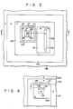
- Fig. 4 is a part of a plan view of another embodiment of the present invention.
- first diffusion region lll is provided along the entire surface junction between inner region l05′ and base region l03
- second diffusion region ll2 is provided along the entire surface junction between inner region l05′ and floating region ll0.
- first and second diffusion regions lll and ll2 may be provided along only the portions of both of the above mentioned surface junctions. This is because the punch through starting voltage is determined at a point where distance l is shortest.
Landscapes
- Thyristors (AREA)
Applications Claiming Priority (2)
| Application Number | Priority Date | Filing Date | Title |
|---|---|---|---|
| JP60261274A JPS62122272A (ja) | 1985-11-22 | 1985-11-22 | 半導体装置 |
| JP261274/85 | 1985-11-22 |
Publications (2)
| Publication Number | Publication Date |
|---|---|
| EP0224091A1 true EP0224091A1 (de) | 1987-06-03 |
| EP0224091B1 EP0224091B1 (de) | 1990-05-23 |
Family
ID=17359541
Family Applications (1)
| Application Number | Title | Priority Date | Filing Date |
|---|---|---|---|
| EP86115431A Expired EP0224091B1 (de) | 1985-11-22 | 1986-11-07 | Halbleiteranordnung mit einem Schutztransistor |
Country Status (4)
| Country | Link |
|---|---|
| US (1) | US4943835A (de) |
| EP (1) | EP0224091B1 (de) |
| JP (1) | JPS62122272A (de) |
| DE (1) | DE3671582D1 (de) |
Cited By (1)
| Publication number | Priority date | Publication date | Assignee | Title |
|---|---|---|---|---|
| WO1996009649A1 (de) * | 1994-09-22 | 1996-03-28 | Daimler-Benz Aktiengesellschaft | Steuerbares halbleiterbauelement |
Families Citing this family (8)
| Publication number | Priority date | Publication date | Assignee | Title |
|---|---|---|---|---|
| US5258641A (en) * | 1989-12-28 | 1993-11-02 | Mitsubishi Denki Kabushiki Kaisha | Semiconductor device for extracting a signal used to monitor potential of a high voltage island at a low voltage island and method of manufacturing the same |
| TW218424B (de) * | 1992-05-21 | 1994-01-01 | Philips Nv | |
| JP3495847B2 (ja) * | 1995-09-11 | 2004-02-09 | シャープ株式会社 | サイリスタを備える半導体集積回路 |
| JP3596830B2 (ja) * | 1995-11-27 | 2004-12-02 | 株式会社ルネサステクノロジ | 半導体装置の入力保護回路 |
| FR2764112B1 (fr) * | 1997-05-28 | 1999-08-13 | Sgs Thomson Microelectronics | Mur d'isolement entre composants de puissance |
| US5949094A (en) * | 1997-08-29 | 1999-09-07 | Texas Instruments Incorporated | ESD protection for high density DRAMs using triple-well technology |
| GB2355110A (en) * | 1999-08-11 | 2001-04-11 | Mitel Semiconductor Ltd | High voltage semiconductor device termination structure |
| FR2819102B1 (fr) * | 2000-12-29 | 2003-04-04 | St Microelectronics Sa | Commutateur electronique bidirectionnel bistable a commande par impulsions |
Citations (1)
| Publication number | Priority date | Publication date | Assignee | Title |
|---|---|---|---|---|
| FR2080988A1 (de) * | 1970-02-13 | 1971-11-26 | Siemens Ag |
Family Cites Families (5)
| Publication number | Priority date | Publication date | Assignee | Title |
|---|---|---|---|---|
| JPS57141962A (en) * | 1981-02-27 | 1982-09-02 | Hitachi Ltd | Semiconductor integrated circuit device |
| JPS57211272A (en) * | 1981-06-23 | 1982-12-25 | Toshiba Corp | Semiconductor device |
| GB2134705B (en) * | 1983-01-28 | 1985-12-24 | Philips Electronic Associated | Semiconductor devices |
| JPS6035571A (ja) * | 1983-08-08 | 1985-02-23 | Sanken Electric Co Ltd | 半導体装置 |
| JPS6074678A (ja) * | 1983-09-30 | 1985-04-26 | Toshiba Corp | 半導体装置 |
-
1985
- 1985-11-22 JP JP60261274A patent/JPS62122272A/ja active Granted
-
1986
- 1986-11-07 EP EP86115431A patent/EP0224091B1/de not_active Expired
- 1986-11-07 DE DE8686115431T patent/DE3671582D1/de not_active Expired - Lifetime
-
1988
- 1988-09-29 US US07/253,364 patent/US4943835A/en not_active Expired - Lifetime
Patent Citations (1)
| Publication number | Priority date | Publication date | Assignee | Title |
|---|---|---|---|---|
| FR2080988A1 (de) * | 1970-02-13 | 1971-11-26 | Siemens Ag |
Non-Patent Citations (2)
| Title |
|---|
| PATENTS ABSTRACTS OF JAPAN, vol. 9, no. 154 (E-325)[1877], 28th June 1985; & JP-A-60 35 571 (SANKEN DENKI K.K.) 23-02-1985 * |
| PATENTS ABSTRACTS OF JAPAN, vol. 9, no. 212 (E-339)[1935], 29th August 1985; & JP-A-60 74 678 (TOSHIBA K.K.) 26-04-1985 * |
Cited By (2)
| Publication number | Priority date | Publication date | Assignee | Title |
|---|---|---|---|---|
| WO1996009649A1 (de) * | 1994-09-22 | 1996-03-28 | Daimler-Benz Aktiengesellschaft | Steuerbares halbleiterbauelement |
| US5923055A (en) * | 1994-09-22 | 1999-07-13 | Daimler-Benz Aktiengesellschaft | Controllable semiconductor component |
Also Published As
| Publication number | Publication date |
|---|---|
| JPS62122272A (ja) | 1987-06-03 |
| DE3671582D1 (de) | 1990-06-28 |
| JPH0154865B2 (de) | 1989-11-21 |
| EP0224091B1 (de) | 1990-05-23 |
| US4943835A (en) | 1990-07-24 |
Similar Documents
| Publication | Publication Date | Title |
|---|---|---|
| JP3180831B2 (ja) | 絶縁ゲート制御半導体装置 | |
| US4697199A (en) | Semiconductor protection device having a bipolar transistor and an auxiliary field effect transistor | |
| JP3168874B2 (ja) | 半導体装置 | |
| KR920010314B1 (ko) | 반도체 장치 | |
| US4016596A (en) | High performance integrated bipolar and complementary field effect transistors | |
| JPH0575110A (ja) | 半導体装置 | |
| US5240865A (en) | Method of forming a thyristor on an SOI substrate | |
| EP0177665B1 (de) | Ausschaltbare Halbleiterschaltvorrichtung | |
| US4943835A (en) | Semiconductor device including protecting MOS transistor | |
| JPS6050960A (ja) | 半導体装置 | |
| US5925900A (en) | Emitter-switched thyristor having a floating ohmic contact | |
| EP0341730B1 (de) | Gate-gesteuerte Zweirichtungshalbleiterschaltungseinrichtung | |
| JPH10505953A (ja) | 制御可能な半導体構成素子 | |
| US5949128A (en) | Bipolar transistor with MOS-controlled protection for reverse-biased emitter-base junction | |
| EP0253353B1 (de) | Zusammengesetzte Halbleiteranordnung | |
| JP2557818B2 (ja) | 逆導通ゲ−トタ−ンオフサイリスタ装置 | |
| JPH0324789B2 (de) | ||
| KR100225381B1 (ko) | 트렌치 캐소드 구조를 갖는 에미터-스위치드 다이리스터 및 그의 제조방법 | |
| JPH0217940B2 (de) | ||
| US5172208A (en) | Thyristor | |
| KR100241055B1 (ko) | 트렌치-게이트 수평형 절연게이트 바이폴라 트랜지스터 | |
| JP3200328B2 (ja) | 複合半導体装置 | |
| KR100222044B1 (ko) | 에미터 스위치 사이리스터 | |
| KR0133556B1 (ko) | 수평형 절연게이트 바이폴라 트랜지스터 | |
| JP2502696B2 (ja) | 半導体集積回路装置 |
Legal Events
| Date | Code | Title | Description |
|---|---|---|---|
| PUAI | Public reference made under article 153(3) epc to a published international application that has entered the european phase |
Free format text: ORIGINAL CODE: 0009012 |
|
| 17P | Request for examination filed |
Effective date: 19861107 |
|
| AK | Designated contracting states |
Kind code of ref document: A1 Designated state(s): DE FR GB |
|
| 17Q | First examination report despatched |
Effective date: 19890123 |
|
| GRAA | (expected) grant |
Free format text: ORIGINAL CODE: 0009210 |
|
| AK | Designated contracting states |
Kind code of ref document: B1 Designated state(s): DE FR GB |
|
| REF | Corresponds to: |
Ref document number: 3671582 Country of ref document: DE Date of ref document: 19900628 |
|
| ET | Fr: translation filed | ||
| PLBE | No opposition filed within time limit |
Free format text: ORIGINAL CODE: 0009261 |
|
| STAA | Information on the status of an ep patent application or granted ep patent |
Free format text: STATUS: NO OPPOSITION FILED WITHIN TIME LIMIT |
|
| 26N | No opposition filed | ||
| REG | Reference to a national code |
Ref country code: GB Ref legal event code: 746 Effective date: 19980917 |
|
| REG | Reference to a national code |
Ref country code: FR Ref legal event code: D6 |
|
| REG | Reference to a national code |
Ref country code: GB Ref legal event code: IF02 |
|
| PGFP | Annual fee paid to national office [announced via postgrant information from national office to epo] |
Ref country code: GB Payment date: 20051102 Year of fee payment: 20 |
|
| PGFP | Annual fee paid to national office [announced via postgrant information from national office to epo] |
Ref country code: DE Payment date: 20051103 Year of fee payment: 20 |
|
| PGFP | Annual fee paid to national office [announced via postgrant information from national office to epo] |
Ref country code: FR Payment date: 20051108 Year of fee payment: 20 |
|
| PG25 | Lapsed in a contracting state [announced via postgrant information from national office to epo] |
Ref country code: GB Free format text: LAPSE BECAUSE OF EXPIRATION OF PROTECTION Effective date: 20061106 |
|
| REG | Reference to a national code |
Ref country code: GB Ref legal event code: PE20 |