EP0224109A1 - Procédé et dispositif pour mettre en oeuvre un onduleur à impulsion avec compensation des temps de tension faussée par l'effet d'accumulation de charge - Google Patents
Procédé et dispositif pour mettre en oeuvre un onduleur à impulsion avec compensation des temps de tension faussée par l'effet d'accumulation de charge Download PDFInfo
- Publication number
- EP0224109A1 EP0224109A1 EP86115586A EP86115586A EP0224109A1 EP 0224109 A1 EP0224109 A1 EP 0224109A1 EP 86115586 A EP86115586 A EP 86115586A EP 86115586 A EP86115586 A EP 86115586A EP 0224109 A1 EP0224109 A1 EP 0224109A1
- Authority
- EP
- European Patent Office
- Prior art keywords
- pulse
- voltage
- valve
- control
- locking
- Prior art date
- Legal status (The legal status is an assumption and is not a legal conclusion. Google has not performed a legal analysis and makes no representation as to the accuracy of the status listed.)
- Withdrawn
Links
- 238000000034 method Methods 0.000 title claims description 13
- 230000000694 effects Effects 0.000 title description 4
- 238000012937 correction Methods 0.000 claims abstract description 16
- 238000005259 measurement Methods 0.000 claims description 17
- 238000011156 evaluation Methods 0.000 claims description 6
- 238000001208 nuclear magnetic resonance pulse sequence Methods 0.000 claims description 3
- 238000001514 detection method Methods 0.000 claims 1
- 230000004913 activation Effects 0.000 abstract 1
- 230000015572 biosynthetic process Effects 0.000 description 2
- 238000005516 engineering process Methods 0.000 description 2
- 230000010354 integration Effects 0.000 description 2
- 230000001276 controlling effect Effects 0.000 description 1
- 238000011161 development Methods 0.000 description 1
- 230000018109 developmental process Effects 0.000 description 1
- 230000001105 regulatory effect Effects 0.000 description 1
- 239000004065 semiconductor Substances 0.000 description 1
- 238000003079 width control Methods 0.000 description 1
Images


Classifications
-
- H—ELECTRICITY
- H02—GENERATION; CONVERSION OR DISTRIBUTION OF ELECTRIC POWER
- H02M—APPARATUS FOR CONVERSION BETWEEN AC AND AC, BETWEEN AC AND DC, OR BETWEEN DC AND DC, AND FOR USE WITH MAINS OR SIMILAR POWER SUPPLY SYSTEMS; CONVERSION OF DC OR AC INPUT POWER INTO SURGE OUTPUT POWER; CONTROL OR REGULATION THEREOF
- H02M7/00—Conversion of AC power input into DC power output; Conversion of DC power input into AC power output
- H02M7/42—Conversion of DC power input into AC power output without possibility of reversal
- H02M7/44—Conversion of DC power input into AC power output without possibility of reversal by static converters
- H02M7/48—Conversion of DC power input into AC power output without possibility of reversal by static converters using discharge tubes with control electrode or semiconductor devices with control electrode
- H02M7/53—Conversion of DC power input into AC power output without possibility of reversal by static converters using discharge tubes with control electrode or semiconductor devices with control electrode using devices of a triode or transistor type requiring continuous application of a control signal
- H02M7/537—Conversion of DC power input into AC power output without possibility of reversal by static converters using discharge tubes with control electrode or semiconductor devices with control electrode using devices of a triode or transistor type requiring continuous application of a control signal using semiconductor devices only, e.g. single switched pulse inverters
- H02M7/5387—Conversion of DC power input into AC power output without possibility of reversal by static converters using discharge tubes with control electrode or semiconductor devices with control electrode using devices of a triode or transistor type requiring continuous application of a control signal using semiconductor devices only, e.g. single switched pulse inverters in a bridge configuration
- H02M7/53871—Conversion of DC power input into AC power output without possibility of reversal by static converters using discharge tubes with control electrode or semiconductor devices with control electrode using devices of a triode or transistor type requiring continuous application of a control signal using semiconductor devices only, e.g. single switched pulse inverters in a bridge configuration with automatic control of output voltage or current
- H02M7/53875—Conversion of DC power input into AC power output without possibility of reversal by static converters using discharge tubes with control electrode or semiconductor devices with control electrode using devices of a triode or transistor type requiring continuous application of a control signal using semiconductor devices only, e.g. single switched pulse inverters in a bridge configuration with automatic control of output voltage or current with analogue control of three-phase output
-
- H—ELECTRICITY
- H02—GENERATION; CONVERSION OR DISTRIBUTION OF ELECTRIC POWER
- H02M—APPARATUS FOR CONVERSION BETWEEN AC AND AC, BETWEEN AC AND DC, OR BETWEEN DC AND DC, AND FOR USE WITH MAINS OR SIMILAR POWER SUPPLY SYSTEMS; CONVERSION OF DC OR AC INPUT POWER INTO SURGE OUTPUT POWER; CONTROL OR REGULATION THEREOF
- H02M1/00—Details of apparatus for conversion
- H02M1/38—Means for preventing simultaneous conduction of switches
- H02M1/385—Means for preventing simultaneous conduction of switches with means for correcting output voltage deviations introduced by the dead time
Definitions
- the invention relates to a method for operating a pulse converter, in particular a pulse converter with transistors or turn-off thyristors (GTO), with the features of the preamble of claim 1 and a device therefor.
- a pulse converter in particular a pulse converter with transistors or turn-off thyristors (GTO), with the features of the preamble of claim 1 and a device therefor.
- GTO turn-off thyristors
- a preferred field of application is the supply of a three-phase machine by means of a pulsed three-phase voltage system.
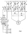
- an asynchronous machine ASM is connected to the terminals P, N of a DC voltage via a pulse inverter.
- the terminal voltages UR, US, UT of the machine can be measured on a corresponding measuring device MU and in a regulating and control unit RZ together with target values f * , U * for frequency and amplitude of the inverter output voltage to a target value for the terminal voltage UR are processed.
- a sinusoidal or trapezoidal course of the phase voltages is generally advantageous, which is predetermined by the course of a corresponding control voltage UR * , for example assigned to phase R, in order to control the valves working on the common inverter-side connection R.
- the control pulses S1, S2 for the valves T1, T2 working on this connection are then derived from UR * .
- the voltage URS can therefore only consist of bipolar, for example sinusoidally wide modulated voltage pulses. In the machine, these lead to a phase current corresponding to the (for example sinusoidal) curve of the control voltage UR * .
- a high pulse frequency for example a few kilo-Hertz, is therefore advantageously specified for the pulsed control of the valves, and transistors or GTO thyristors are advantageously used as correspondingly fast-switching converter valves.
- the control pulses SI, S2 are derived from a pulse-width-modulated control voltage UM * , which a pulse-width modulator PM forms by scanning the control voltage UR * with a high-frequency, usually triangular, pulse voltage.
- valve Tl needs a certain time after its control pulse S1 has been removed until its conductive state has ended and therefore no current can flow from the terminal P via the valve Tl, but rather the current in phase R from the valve Tl to the valve T2 or (if T2 is blocked) the freewheel valve V2 is commutated.
- a "storage time" ST1 which is characteristic of the valve T1
- the conductive state is stored even after the control pulse S1 has been removed, and the phase voltage UR is only then switched through from the positive terminal voltage to the negative terminal voltage.
- valve T2 must not yet be activated in order to avoid a short circuit in the DC voltage.
- these valves When the valves are actuated alternately, these valves must therefore be temporarily locked together between two pulse-width-modulated control pulses with which they are actuated alternately.
- This locking is carried out by a corresponding circuit (not shown in detail) in the pulse evaluation PA.
- a constant locking time is set, which must then be greater than the maximum storage time possible in one of the two valves.
- the control pulses S1 and S2 are each shorter by the locking time VT than the binary states of the pulse-width-modulated control voltage UM * from which they are derived.
- the control pulses therefore describe a pulse width modulated curve, the amplitude of which corresponds according to the locking times VT and the number of locking operations carried out within a UR * period. This reduction can be taken into account in the formation of UR * or UM * and thus in the pulse width control for the control pulses.
- the actual voltage UR is not affected by the locking width VT, but by the difference VT - ST1 when the current commutates from T1 or the difference from V T - ST2 when the current commutes from T2.
- the storage times of a semiconductor valve are subject to strong sample variations and can also change depending on the load.
- the object of the invention is to avoid such distortions caused by carrier-memory effects during the locking times.
- FIG. 2 first shows the course of the unmodulated control voltage UR * and the high-frequency keying voltage UD, from the intersections of which the pulse width modulator PM forms the pulse width modulated control voltage UM * .
- valve voltage UT2 can be understood as a binary actual value signal to which the setpoint signal S1 is assigned. They coincide up to the point in time T1 at which the control pulse S1 ends.
- the current previously flowing through T1 now requires the storage time ST1 until it can commute to the freewheeling diode V2 or the then ignited valve T2.
- the valve voltage UT2 or the voltage UR therefore only breaks down at the time t1 + ST1.
- the control pulses S1, S2 remain for the duration of the locking time VT both valves T1, T2 are locked together and the control pulse S2 is only released with the time shift given by the locking time VT after the pulse edge of the pulse-width-modulated control voltage UM * .
- valve T1 At time t2, the current should be commutated back to valve T1 in accordance with the pulse edge of U M * , and control pulse S2 is ended. S1, however, remains locked for the duration of the locking time VT.
- the valve voltage UT1 of the valve T1 which is again shown as a binary actual value, only changes to the initial state at the time t2 + ST2, since the valve T2 is still conductive during the storage time ST2.
- a voltage time area UF2 is also created.
- the voltage at the connection R can be detected directly as a common measure for the respective valve voltages. In particular, it is sufficient to detect only a binary signal as the measured value for the valve voltages or this connection voltage. The actual voltage is preferably detected potential-free. It can then be compared in a simple manner with the control pulses.
- the corresponding binary setpoints are given by the control pulse sequences S1, S2 or by the pulse-width-modulated control voltage UM * on which the control pulses are based,
- FIG. 2 shows the course UR of the smoothed connection voltage.
- a cycle clock pulse PT is shown, which in each case initiates a new Altern michszyklus to form ehlwoodszeit inhabit to the difference of the F occur within a cycle.
- this pulse PT is derived from the negative amplitude of the keying voltage UD , but it can also be derived from the edges of the control pulses or in some other way.
- a positive difference signal UM * - UR therefore represents a measuring pulse which characterizes the conductive state of the valve T1 and whose duration is equal to the storage time ST1.
- a negative difference signal represents a measuring pulse for the conductive state of the valve T2.
- a polarity signal PP is also indicated in FIG. 2, which consists of suitable pulse edges, e.g. the negative edge of UR.
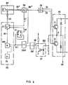
- a first, constructed in analog circuit embodiment of the invention is shown that the strength of F already.
- the pulse converter PR with its its terminal AC voltage UR associated valves Tl, T2, and the free-wheeling valves V1 and V2, and consisting of the pulse width modulator PM and the P ulsausêt PA modulation stage.
- the control voltage UR * is connected to an adder AD with a correction variable derived from the output signal UF of an integrator INT.
- the voltage UR is detected by the valve voltage measuring device MU as a measurement signal that represents the conductive state of a controlled valve.
- the subtraction circuit SUB is first considered, in which the setpoint for the valve voltages specified by UM * is compared with the actual value detected by UR, in order then to the integrator INT to form the voltage time area that occurs during a locking time will.
- MT is a switching pulse that is not supplied to the integrator input, but rather to the control input of a switch SW, and releases the integrator input at most during a locking time. Actual voltage values UR recorded outside the locking time are therefore out of engagement for the determination of the correction variable.
- a binary signal can also be integrated in the integrator, which occurs only during a locking time and ends with the end of the conductive state of a valve. This is the case for the measuring pulse MT, which is therefore equivalent to the difference UM * - UR.
- the gate EXOR assumes the role of the subtraction element SUB, provided the polarity signal PP is used to take into account the polarity reversal of the measurement signal UR that occurs during a locking time by means of a corresponding sign evaluation at the integrator input.
- the subtraction element SUB with its inputs and outputs is superfluous in this case.
- control unit RZ is replaced by a microprocessor MP, which supplies the unmodulated control voltage UR * from digitally entered setpoints and actual values, taking into account the correction signal UF, which is now also digitally input.
- the pulse width modulator PM and the pulse evaluation PA form the control pulses S1 and S2.
- the valve voltage measuring device contains an optocoupler OP for the potential-free measurement of the valve voltages, both valve voltages being detected jointly on the basis of the described relationships by the voltage UR at their common connection point.
- An inverting element INV forms a binary measurement signal, the signal state H of which thus identifies the conductive state of a valve.
- an up-down counter CT is provided for the pulses of a counting pulse generator OS, the pulse frequency of which can be, for example, a few M Hz and which therefore has a small pulse period compared to the locking times.
- the input of this counter is released by an AND gate AND only if it coincides with the measuring pulse MT, while the counting direction is determined by the polarity signal PP.
- This polarity signal PP is formed by means of a D flip-flop from the edges of the measuring pulse MT in such a way that the counting direction is reversed after two locking times.
- the invention thus makes it possible, by means of a relatively simple additional device, in particular in the case of transistor pulse converters, to avoid distortion of the AC output voltage caused by the carrier-memory effect.
Landscapes
- Engineering & Computer Science (AREA)
- Power Engineering (AREA)
- Magnetically Actuated Valves (AREA)
- Inverter Devices (AREA)
Applications Claiming Priority (2)
| Application Number | Priority Date | Filing Date | Title |
|---|---|---|---|
| DE19853541227 DE3541227A1 (de) | 1985-11-21 | 1985-11-21 | Verfahren und vorrichtung zum betrieb eines pulsumrichters mit kompensation von durch traeger-speicher-effekte hervorgerufenen fehlspannungszeitflaechen |
| DE3541227 | 1985-11-21 |
Publications (1)
| Publication Number | Publication Date |
|---|---|
| EP0224109A1 true EP0224109A1 (fr) | 1987-06-03 |
Family
ID=6286511
Family Applications (1)
| Application Number | Title | Priority Date | Filing Date |
|---|---|---|---|
| EP86115586A Withdrawn EP0224109A1 (fr) | 1985-11-21 | 1986-11-10 | Procédé et dispositif pour mettre en oeuvre un onduleur à impulsion avec compensation des temps de tension faussée par l'effet d'accumulation de charge |
Country Status (4)
| Country | Link |
|---|---|
| US (1) | US4730246A (fr) |
| EP (1) | EP0224109A1 (fr) |
| DE (1) | DE3541227A1 (fr) |
| FI (1) | FI862799A7 (fr) |
Cited By (1)
| Publication number | Priority date | Publication date | Assignee | Title |
|---|---|---|---|---|
| DE4016286A1 (de) * | 1990-05-21 | 1991-11-28 | Bosch Gmbh Robert | Verfahren zur impulsbreitenmodulation fuer einen umrichter |
Families Citing this family (6)
| Publication number | Priority date | Publication date | Assignee | Title |
|---|---|---|---|---|
| FI77547C (fi) * | 1986-03-19 | 1989-03-10 | Kone Oy | Foerfarande och anordning foer reglering av styrspaenningen vid en trefasig inventer som matar en vaexelstroemmotor. |
| DE4018930C2 (de) * | 1990-06-13 | 1994-07-14 | Klug Rolf Dieter Dr Ing | Brückenzweig von Gleichstromstellern und Pulswechselrichtern mit geregeltem Querstrom |
| US5892673A (en) * | 1996-03-25 | 1999-04-06 | General Electric Company | Robust, high-density, high-efficiency state sequence controller for an auxiliary resonant commutation pole power converter |
| IT1306069B1 (it) * | 1998-11-20 | 2001-05-29 | Zapi Spa | Procedimento di alimentazione di motori asincroni con inverter,inparticolare per veicoli a batteria |
| JP4689905B2 (ja) * | 2001-08-29 | 2011-06-01 | サンデン株式会社 | ブラシレスモータの駆動制御方法及びその装置 |
| FR3035557B1 (fr) * | 2015-04-23 | 2017-05-12 | Labinal Power Systems | Systeme et procede de dissipation de l'energie electrique regeneree par des actionneurs |
Citations (2)
| Publication number | Priority date | Publication date | Assignee | Title |
|---|---|---|---|---|
| EP0085541A1 (fr) * | 1982-01-28 | 1983-08-10 | Fanuc Ltd. | Appareil de commande de moteur synchrone |
| EP0121575A1 (fr) * | 1982-10-19 | 1984-10-17 | Fanuc Ltd. | Controleur de moteur |
Family Cites Families (5)
| Publication number | Priority date | Publication date | Assignee | Title |
|---|---|---|---|---|
| US3710229A (en) * | 1971-06-11 | 1973-01-09 | Westinghouse Electric Corp | Integrator controlled inverter |
| US4150423A (en) * | 1977-09-19 | 1979-04-17 | Boschert Associates | Transformer coupled pass element |
| US4447867A (en) * | 1982-01-29 | 1984-05-08 | Varo, Inc. | Multiphase inverter drive circuit with synchronized switching delay feature |
| US4535399A (en) * | 1983-06-03 | 1985-08-13 | National Semiconductor Corporation | Regulated switched power circuit with resonant load |
| US4633381A (en) * | 1985-02-26 | 1986-12-30 | Sundstrand Corporation | Inverter shoot-through protection circuit |
-
1985
- 1985-11-21 DE DE19853541227 patent/DE3541227A1/de not_active Withdrawn
-
1986
- 1986-07-01 FI FI862799A patent/FI862799A7/fi not_active Application Discontinuation
- 1986-10-03 US US06/915,082 patent/US4730246A/en not_active Expired - Fee Related
- 1986-11-10 EP EP86115586A patent/EP0224109A1/fr not_active Withdrawn
Patent Citations (2)
| Publication number | Priority date | Publication date | Assignee | Title |
|---|---|---|---|---|
| EP0085541A1 (fr) * | 1982-01-28 | 1983-08-10 | Fanuc Ltd. | Appareil de commande de moteur synchrone |
| EP0121575A1 (fr) * | 1982-10-19 | 1984-10-17 | Fanuc Ltd. | Controleur de moteur |
Cited By (1)
| Publication number | Priority date | Publication date | Assignee | Title |
|---|---|---|---|---|
| DE4016286A1 (de) * | 1990-05-21 | 1991-11-28 | Bosch Gmbh Robert | Verfahren zur impulsbreitenmodulation fuer einen umrichter |
Also Published As
| Publication number | Publication date |
|---|---|
| FI862799A7 (fi) | 1987-05-22 |
| US4730246A (en) | 1988-03-08 |
| FI862799A0 (fi) | 1986-07-01 |
| DE3541227A1 (de) | 1987-05-27 |
Similar Documents
| Publication | Publication Date | Title |
|---|---|---|
| DE10237882B4 (de) | Verfahren zur Impulsbreitenmodulation, Spannungswandler und Wechselrichter | |
| DE3134002C2 (de) | Vorrichtung zur Steuerung der Drehzahl eines Induktionsmotors | |
| DE3712185A1 (de) | Laststromerfassungseinrichtung fuer stromrichter mit pulsdauermodulation | |
| DE3101102C2 (fr) | ||
| DE2757463A1 (de) | Transistorwechselrichter mit einem leistungstransformator | |
| DE19716891A1 (de) | Wechselrichtervorrichtung des Spannungstyps und Verfahren zu deren Steuerung | |
| DE3914863A1 (de) | Steuersystem fuer einen kraftfahrzeugladegenerator | |
| DE3841147A1 (de) | Verfahren zum ansteuern eines wechselstrom-motors sowie nach diesem verfahren ansteuerbarer wechselstrom-motor | |
| DE3306983C2 (fr) | ||
| CH663124A5 (de) | Induktionsmotor-regelverfahren und -anordnung. | |
| DE3541227A1 (de) | Verfahren und vorrichtung zum betrieb eines pulsumrichters mit kompensation von durch traeger-speicher-effekte hervorgerufenen fehlspannungszeitflaechen | |
| DE2115393A1 (de) | Servomotor Steuerschaltung | |
| EP0212462A2 (fr) | Circuit d'amplificateur pour électro-aimants de valves proportionnelles ou de servo-valves | |
| DE3529591A1 (de) | Verfahren und vorrichtung zum betrieb eines wechselrichters | |
| DE2705343C2 (de) | Steuerverfahren für einen selbstgeführten, pulsgesteuerten Wechselrichter und Steueranordnung zur Bildung der Sollwerte für die Pulssteuerung | |
| EP0898360B1 (fr) | Méthode pour la commande d'un survolteur à un circuit intermédiaire de tension alternative et appareil pour le même | |
| EP0458055A2 (fr) | Procédé de modulation d'impulsions en durée pour convertisseur | |
| DE2744484C2 (de) | Spannungsgeregelter Pulsmodulator | |
| EP0142649A2 (fr) | Procédé et dispositif pour la commande de commutateurs dans un onduleur polyphasé, en particulier dans un onduleur à transistors | |
| DE2554223C3 (de) | Steuereinrichtung zur Aufrechterhaltung der Stabilität eines Wechselrichters | |
| DE2408381C3 (de) | Schaltungsanordnung zur pulsbreitenmodulierten Ansteuerung von Leistungstransistoren | |
| DE3017885C2 (de) | Gleichstromversorgungseinrichtung | |
| DE102015203816A1 (de) | Verfahren und Vorrichtung zum Erkennen eines Ansteuerverfahrens eines Wechselrichters | |
| DE102019218940A1 (de) | Dreiphasen-wechselstromsteuervorrichtung und dreiphasen-wechselstromsteuersystem | |
| DE3310816C2 (fr) |
Legal Events
| Date | Code | Title | Description |
|---|---|---|---|
| PUAI | Public reference made under article 153(3) epc to a published international application that has entered the european phase |
Free format text: ORIGINAL CODE: 0009012 |
|
| AK | Designated contracting states |
Kind code of ref document: A1 Designated state(s): AT CH DE GB IT LI SE |
|
| 17P | Request for examination filed |
Effective date: 19870708 |
|
| 17Q | First examination report despatched |
Effective date: 19890222 |
|
| STAA | Information on the status of an ep patent application or granted ep patent |
Free format text: STATUS: THE APPLICATION IS DEEMED TO BE WITHDRAWN |
|
| 18D | Application deemed to be withdrawn |
Effective date: 19891014 |
|
| RIN1 | Information on inventor provided before grant (corrected) |
Inventor name: SCHWESIG, GUENTER, DIPL.-ING. |