EP0458055A2 - Procédé de modulation d'impulsions en durée pour convertisseur - Google Patents
Procédé de modulation d'impulsions en durée pour convertisseur Download PDFInfo
- Publication number
- EP0458055A2 EP0458055A2 EP19910105924 EP91105924A EP0458055A2 EP 0458055 A2 EP0458055 A2 EP 0458055A2 EP 19910105924 EP19910105924 EP 19910105924 EP 91105924 A EP91105924 A EP 91105924A EP 0458055 A2 EP0458055 A2 EP 0458055A2
- Authority
- EP
- European Patent Office
- Prior art keywords
- switching
- power transistors
- pulse
- voltage
- signal
- Prior art date
- Legal status (The legal status is an assumption and is not a legal conclusion. Google has not performed a legal analysis and makes no representation as to the accuracy of the status listed.)
- Withdrawn
Links
Images


Classifications
-
- H—ELECTRICITY
- H02—GENERATION; CONVERSION OR DISTRIBUTION OF ELECTRIC POWER
- H02M—APPARATUS FOR CONVERSION BETWEEN AC AND AC, BETWEEN AC AND DC, OR BETWEEN DC AND DC, AND FOR USE WITH MAINS OR SIMILAR POWER SUPPLY SYSTEMS; CONVERSION OF DC OR AC INPUT POWER INTO SURGE OUTPUT POWER; CONTROL OR REGULATION THEREOF
- H02M7/00—Conversion of AC power input into DC power output; Conversion of DC power input into AC power output
- H02M7/42—Conversion of DC power input into AC power output without possibility of reversal
- H02M7/44—Conversion of DC power input into AC power output without possibility of reversal by static converters
- H02M7/48—Conversion of DC power input into AC power output without possibility of reversal by static converters using discharge tubes with control electrode or semiconductor devices with control electrode
- H02M7/53—Conversion of DC power input into AC power output without possibility of reversal by static converters using discharge tubes with control electrode or semiconductor devices with control electrode using devices of a triode or transistor type requiring continuous application of a control signal
- H02M7/537—Conversion of DC power input into AC power output without possibility of reversal by static converters using discharge tubes with control electrode or semiconductor devices with control electrode using devices of a triode or transistor type requiring continuous application of a control signal using semiconductor devices only, e.g. single switched pulse inverters
- H02M7/539—Conversion of DC power input into AC power output without possibility of reversal by static converters using discharge tubes with control electrode or semiconductor devices with control electrode using devices of a triode or transistor type requiring continuous application of a control signal using semiconductor devices only, e.g. single switched pulse inverters with automatic control of output wave form or frequency
- H02M7/5395—Conversion of DC power input into AC power output without possibility of reversal by static converters using discharge tubes with control electrode or semiconductor devices with control electrode using devices of a triode or transistor type requiring continuous application of a control signal using semiconductor devices only, e.g. single switched pulse inverters with automatic control of output wave form or frequency by pulse-width modulation
-
- H—ELECTRICITY
- H02—GENERATION; CONVERSION OR DISTRIBUTION OF ELECTRIC POWER
- H02M—APPARATUS FOR CONVERSION BETWEEN AC AND AC, BETWEEN AC AND DC, OR BETWEEN DC AND DC, AND FOR USE WITH MAINS OR SIMILAR POWER SUPPLY SYSTEMS; CONVERSION OF DC OR AC INPUT POWER INTO SURGE OUTPUT POWER; CONTROL OR REGULATION THEREOF
- H02M7/00—Conversion of AC power input into DC power output; Conversion of DC power input into AC power output
- H02M7/42—Conversion of DC power input into AC power output without possibility of reversal
- H02M7/44—Conversion of DC power input into AC power output without possibility of reversal by static converters
- H02M7/48—Conversion of DC power input into AC power output without possibility of reversal by static converters using discharge tubes with control electrode or semiconductor devices with control electrode
- H02M7/53—Conversion of DC power input into AC power output without possibility of reversal by static converters using discharge tubes with control electrode or semiconductor devices with control electrode using devices of a triode or transistor type requiring continuous application of a control signal
- H02M7/537—Conversion of DC power input into AC power output without possibility of reversal by static converters using discharge tubes with control electrode or semiconductor devices with control electrode using devices of a triode or transistor type requiring continuous application of a control signal using semiconductor devices only, e.g. single switched pulse inverters
- H02M7/538—Conversion of DC power input into AC power output without possibility of reversal by static converters using discharge tubes with control electrode or semiconductor devices with control electrode using devices of a triode or transistor type requiring continuous application of a control signal using semiconductor devices only, e.g. single switched pulse inverters in a push-pull configuration
-
- H—ELECTRICITY
- H03—ELECTRONIC CIRCUITRY
- H03K—PULSE TECHNIQUE
- H03K17/00—Electronic switching or gating, i.e. not by contact-making and –breaking
- H03K17/14—Modifications for compensating variations of physical values, e.g. of temperature
-
- H—ELECTRICITY
- H03—ELECTRONIC CIRCUITRY
- H03K—PULSE TECHNIQUE
- H03K17/00—Electronic switching or gating, i.e. not by contact-making and –breaking
- H03K17/51—Electronic switching or gating, i.e. not by contact-making and –breaking characterised by the components used
- H03K17/56—Electronic switching or gating, i.e. not by contact-making and –breaking characterised by the components used by the use, as active elements, of semiconductor devices
- H03K17/60—Electronic switching or gating, i.e. not by contact-making and –breaking characterised by the components used by the use, as active elements, of semiconductor devices the devices being bipolar transistors
- H03K17/66—Switching arrangements for passing the current in either direction at will; Switching arrangements for reversing the current at will
Definitions
- the invention relates to a method according to the preamble of patent claim 1.
- converter output currents can be generated with a high degree of efficiency in accordance with a strongly variable setpoint. Due to the storage time when the switching transistors are switched off, there are longer switch-on signals at the converter output. This leads to problems that have to be taken into account when controlling or generating the pulse-width-modulated switching signals. It is particularly important to ensure that the switching transistor in the other bridge branch is not switched on during the extended switch-on time and that a short-circuit current which is too great is thereby generated. To avoid this it is known, e.g. B.
- EP-PS 01 24 619 via timers to provide a lock that blocks the switching on of the other switching transistor for a predetermined time after the completion of each switch-on pulse.
- this locking takes place via AND gates through a hysteresis circuit with the aid of RC elements. Since the storage time of the switching transistors depends on the temperature, the voltage and the current, and above all increases disproportionately with large load currents and high chip temperature, the two switching transistors must be one Half-bridge can be locked against each other by means of a dead time that corresponds to the maximum possible storage time plus a safety time.
- the object is achieved to adapt the dead time of the switching transistors to the actual switching and / or storage time, as it arises in the current operating state.
- a switching voltage is generated from the base-emitter voltage of the switching transistors, and this is used to lock the other switching transistor of the bridge branch during the storage time currently in progress.
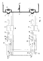
- Fig. 1 two high-voltage power transistors 1 and 2 of a bridge arm are switched from driver stages 3 and 4 in the blocked or saturated region.
- the collector of the power transistor 1 is connected to the positive pole of the supply voltage L + of the power section
- the emitter is connected to the collector of the power transistor 2 of the other bridge branch, the emitter of which is connected to the negative pole L- of the supply voltage.
- U A At the emitter-collector connection 5 between the two transistors 1 and 2 there is the output voltage U A , which is led to a load.
- This bridge branch switched in a known manner can be part of a bridge circuit which, for. B. is in triplicate at the positive and negative output of a DC link and their respective emitter-collector connections 5 is at a winding end of a three-phase winding for a servo motor.
- the control of the power transistors 1 and 2 via the driver stages 3 and 4 and the construction of these driver stages can be carried out in the same way as is shown in DE-OS 35 22 429.
- the switching signals are fed to driver stages 3 and 4 in the same way via electrical isolation stages 8 and 9.
- the base-emitter voltage is tapped at each of the two power transistors 1 and 2 and each is fed to the input of a step trigger 12 and 13 via a further potential isolating stage 10 and 11.
- the output of the step trigger 12 for the base-emitter voltage of the power transistor 1 connected to the positive supply voltage L + is connected to the R input of a D flip-flop 14 and to the first input of an OR gate 15.
- the pulse-width-modulated control signal X is applied, which is fed via a negator 16 and a further OR gate 17 to the negated input of the potential isolation stage 8 and further via a further OR gate 18 with the Input of the potential isolation stage 9 is connected.
- the control signal X can be generated in a known manner in a microprocessor and / or counter stages or by voltage comparison with a delta voltage. If it assumes a high level, a low level is applied via the negator 16 to the input of the potential isolation stage 8, which, for. B. via a light-emitting diode of an optocoupler with its other end at the positive pole of a supply voltage (not shown), a signal to the input of driver stage 3 given that the power transistor 1 controls in the saturation range.
- the base of the power transistor assumes a voltage which is positive with respect to the emitter and which sets the output of the Schmitt trigger 12 to a high level via the potential isolating stage 10.
- control signal X switches to a low level, a high level reaches the input of the potential isolation stage 8 via the negator 16, as a result of which the power transistor 1 is opened or switched to a high-resistance state via the driver stage 3.
- switching to this state does not take place immediately, but in a known manner only after a storage time has elapsed, the time period of which depends on the temperature in the power transistor, the voltages applied to it and the currents flowing through it. This storage time increases disproportionately, especially with large currents. As long as a current flows through the power transistor 1, that is to say also during the storage time, a voltage drop occurs at the base-emitter path, which drops to a high level at the output of the Schmitt trigger 12.
- the control signal at the D input is retained until after the storage time at the Q output of the D flip-flop.
- the time of the output signal UA * applied to this Q output therefore largely corresponds to the time of the output voltage U A applied to the load. So that this correspondence is also given with a different current direction or changing current direction by the load, it will be necessary, as will be explained later, to make the switching of the D flip-flop 14 dependent on a clock pulse which is caused by the positive edges of the Output signals of the two Schmitt triggers 12 and 13 is effected.
- the output signals from the Schmitt triggers 12 and 13 are led to the OR gate, the output of which is connected to the clock input of the D flip-flop via a time stage 19.
- the time step delays the signal only insignificantly, but ensures that the signals are safely applied to the R and S inputs before a clock is generated.
- the power transistor 7 can be controlled to saturation, provided that no current flows through the freewheeling diode 7, which also applies to the power transistor 1 when a current flows through the diode 6, such as will be explained later.
- the output voltage UA * on the D flip-flop 14 can now be used when generating the control signal, for. B. by a corresponding intervention in the control circuit to carry out a correction, since this corresponds to the actual duty cycle of the power transistors 1 and / or 2.
- the output signal of the Schmitt triggers 12 and 13 is further fed to the second input of the OR gate 17 or 18 of the other bridge branch and ensures that a high level is present at the output of the respective OR gate 17 or 18 as long as a current flows through the power transistor 1 or 2 of the other bridge branch, the actual storage time of the power transistors 1 and 2 also being detected.
- a correction of the storage time of the power transistors 1 and 2 is provided in FIG. 2 for a power stage switched and driven in the same way (the same reference numbers are used).
- the other bridge branch is locked in the same way via the Schmitt triggers 12 and 13 and the OR gates 17 and 18.
- the control of the OR gate 17 takes place here instead of the negator 16 via a NAND gate 20, the second one Input at the output of an up / down counter 21 is.
- the control input X is fed to the UP input of this up / down counter 21 and the DOWN input is connected to the output of the Schmitt trigger 12.
- the clock pulses supplied to a clock input CLK of a higher-frequency pulse series, e.g. B. from a microprocessor, the counter being set to zero by a signal at the clear input CL can be.
- This clear input CL is connected to the output of the Schmitt trigger 13 of the other bridge branch.
- a high level is always present at the output 22 of the up / down counter 21 when the counter contains zero or positive values. If the control signal X is positive, a switching signal with a counter reading of zero reaches the driver stage 3 via the NAND gate 20 and the OR gate 17, which switches the power transistor 1 into the saturation range. A short count is made until a corresponding signal from the base-emitter voltage reaches the DOWN input of the up / down counter 21 via the Schmitt trigger 12, whereby essentially the switch-on delay time of the power transistor 1, which is considerably shorter than the switch-off storage time, is recorded. The now positive output signal at the Schmitt trigger 12 stops the counting up, or there is an up / down counting with the same clock pulses, since the DOWN input is now also activated.
- the control of the power transistor 2 takes place with the low level of the control signal X, which is connected via a negator 23 to the UP input of a further up / down counter 24, the clock input CLK of which are supplied with the same clock signals and at the latter DOWN input, the output signals of the Schmitt trigger 13 are.
- the output 25 of the up / down counter 24 constructed in the same way outputs a high level to an input of a further NAND gate 26 whenever the counter reading is zero or positive.
- the control signals inverted via the inverter 23 are delayed in the same way as the control signals for the first bridge branch. If the current at the output UA changes with the other bridge branch when the current direction changes, the up / down counter is set to zero when the other power transistor is switched through.
- FIG. 3 shows a circuit that solves both tasks according to FIG. 1 and FIG. 2. 1 (with the same reference numbers) are connected to one another in the same way, the timing element 19 in front of the clock input of the D flip-flop 14 consisting of two successive negators.
- the isolating stages 8 to 11 are provided with optocouplers, the base of the respective power transistor 1 or 2 being located at a light-emitting diode input of the isolating stages 10 and 11 for detecting the base-emitter voltage.
- the cathode of a diode 31 and 32 is connected to the emitter of the power transistors 1 and 2, and a respective resistor 33 and 34 is connected in parallel.
- the anode of the diodes 31 and 32 lies in each case on the anode of a further diode 35 and 36, the cathode of which is connected to the second light-emitting diode input of the respective isolating stage 10 and 11 is.
- the connection of the two diodes 31 with 35 and 32 with 36 is connected via a capacitor 37 and 38 to the base of the power transistor 1 and 2, respectively.
- the resistor 33 and 34 is dimensioned so that with a high-impedance switched power transistor 1 or 2 with a negative base voltage from the driver stages 3 or 4 a predetermined current through the respective light-emitting diode of the isolating stages 10 or 11, the diode 35 or 36 and the resistor 33 or 34 flows, which causes a positive supply voltage via a resistor 39 or 40 at the output of the isolating stage 10 or 11 to break down to zero.
- the counter stages 21 and 24 according to FIG. 2 are replaced here by a commercially available binary counter 42 and 43 (e.g. an integrated circuit 4520) and a programmable downward binary counter 44 and 45 (e.g. an integrated circuit 4526) , whereby during the storage time of the corresponding power transistors 1 or 2 the respective binary counter 42 or 43 counts up clock pulses, with this number the respective binary counter 44 or 45 is programmed and the switching through is delayed with the next switching pulse until the programmed value returns to zero is counted down.
- a clock pulse signal according to FIG. 2 is fed to each clock input of the four binary counters 42 to 45.
- An increment of binary counters 42 or 43 always occurs only when there is a positive signal at the output of an AND gate 48 or 49, which is also connected to the enable input of the AND gate 48 or 49, also assumes a positive value. However, this is essentially only the case during the storage time of the corresponding power transistor 1 or 2.
- the binary counter 42 or 43 With each negative switch-on pulse edge at the output of the OR gate 17 or 18, the binary counter 42 or 43 is set to zero via a clear input CL via an amplifier 50 or 51, a capacitor 52 or 53 and a negator 54 or 55. At the input of the negators 54 and 55 there is in each case the anode of a diode 56, 57 and a resistor 58, 59, which have their other end or the cathode at the positive pole of the supply voltage. This suppresses the positive edge of the switching voltage.
- a delay circuit consisting of a resistor 62 or 63 with a diode 64 or 65 connected in parallel, one at the input of the OR -Gatter lying capacitor 66 and 67 charges.
- This delay circuit causes the front positive pulse edge to reach the OR gate 17 or 18 without delay, but the rear negative pulse edge has a sufficiently positive signal present at the input of the OR gate 17 or 18 for a while. This ensures that the respective power transistor 1 or 2 remains blocked until the other power transistor 2 or 1 is completely switched into the high-resistance range.
- the power transistors 1 and 2 can consist of several power transistors interconnected in a known manner, and the load at the output U A can be a strongly inductive load, e.g. B. the phase winding of a servo motor.
- the load at the output U A can be a strongly inductive load, e.g. B. the phase winding of a servo motor.
- voltages and currents result in the circuits according to FIGS. 1 to 3, as occur in FIGS. 4 to 6 with different load currents.
- the control signal X and a positive load current I is shown.
- the load current I should increase during the time t 3 to t 1 with the positive control signal X via the power transistor 1 controlled in the saturation range. Due to the storage time of this power transistor 1, a changeover to the high-resistance region takes place only at time t 2. Without a correction of this storage time (t1 to t2), a current I * would form, which rises continuously.
- the base-emitter voltage BE1 and BE2 of the two power transistors 1 and 2 is detected and from this a switching voltage S1 and S2 present behind the Schmitt trigger 12 and 13 is obtained.
- the switch-on delay compared to the storage time usually does not play a significant role in the power transistors (the switch-on delay is, for example, 1 to 2 usec. While the storage time is 20 to 30 usec.) And the storage time is considerably longer, in particular of the load current I and the semiconductor temperature depends on the power transistors, a circuit according to FIG. 3 can be selected.
- a switching voltage Sp1 and Sp2 is generated at the output of the AND gates 48, 49, which has positive pulses that are largely present only during the storage time.
- the corresponding binary counter 42 or 43 is incremented and the corresponding programmable binary counter 44 or 45 is programmed with the incremented value.
- the next switch-on pulse is then passed on to the OR gate 17 or 18 only when the programmed value has been counted down again via the clock pulses.
- an output voltage signal UA * can also be generated from the switching signals S1 and S2, which according to FIG. 1 can be used to correct the generation of the actuating signal or according to FIG. 3 with a corrected one 4 for an additional correction, z. B. serve the curve shape for a sinusoidal total output current I in the control loop.
- Fig. 6 shows the same voltages and currents with changing load current I.
- the control signal X goes to zero and switches off the power transistor 1, the base-emitter voltage BE1 of this power transistor 1 being a negative after the storage time (t1 to t2) Assumes value.
- a current flows through the freewheeling diode 7 until the current I becomes zero.
- the power transistor 2 can turn on and the base-emitter voltage BE2 becomes positive.
- the counting up during which it is not possible to switch through during the freewheeling diode current, does not have any disadvantageous effects.
- the storage capacity does not need to be designed for this time, it is sufficient if it covers the maximum possible switch-on delay or storage time. 3 is counted up only during the duration of the storage time signals Sp1 or Sp2 at the output of the AND gate 48 or 49 and the counting out of the programmable binary counter 44 or 45 begins at the beginning of the corresponding pulse of the actuating signal X, this is done in the time in which switching is not possible due to the freewheeling diode current, so that there is no effect on the switching times of the power transistors.
Landscapes
- Engineering & Computer Science (AREA)
- Power Engineering (AREA)
- Inverter Devices (AREA)
Applications Claiming Priority (2)
| Application Number | Priority Date | Filing Date | Title |
|---|---|---|---|
| DE4016286 | 1990-05-21 | ||
| DE19904016286 DE4016286A1 (de) | 1990-05-21 | 1990-05-21 | Verfahren zur impulsbreitenmodulation fuer einen umrichter |
Publications (2)
| Publication Number | Publication Date |
|---|---|
| EP0458055A2 true EP0458055A2 (fr) | 1991-11-27 |
| EP0458055A3 EP0458055A3 (en) | 1992-03-25 |
Family
ID=6406858
Family Applications (1)
| Application Number | Title | Priority Date | Filing Date |
|---|---|---|---|
| EP19910105924 Withdrawn EP0458055A3 (en) | 1990-05-21 | 1991-04-13 | Pulse width modulation method for a convertor |
Country Status (2)
| Country | Link |
|---|---|
| EP (1) | EP0458055A3 (fr) |
| DE (1) | DE4016286A1 (fr) |
Cited By (4)
| Publication number | Priority date | Publication date | Assignee | Title |
|---|---|---|---|---|
| WO1996033548A1 (fr) * | 1995-04-21 | 1996-10-24 | Gec Alsthom Acec Transport S.A. | Procede de traitement d'ondes pwm et dispositifs appliquant ce procede |
| RU2165125C1 (ru) * | 1999-10-19 | 2001-04-10 | Ульяновский государственный технический университет | Транзисторный преобразователь |
| RU2321148C1 (ru) * | 2006-10-18 | 2008-03-27 | Общество с ограниченной ответственностью Конструкторское Бюро "Системотехника" | Устройство для регулирования выходного тока импульсного стабилизирующего преобразователя |
| RU2539560C1 (ru) * | 2013-11-26 | 2015-01-20 | Общество с ограниченной ответственностью "СЗЛ" | Преобразователь постоянного напряжения в постоянное напряжение |
Families Citing this family (2)
| Publication number | Priority date | Publication date | Assignee | Title |
|---|---|---|---|---|
| JP4044861B2 (ja) * | 2003-04-03 | 2008-02-06 | 三菱電機株式会社 | 電力変換装置およびその電力変換装置を備える電力変換システム装置 |
| DE102009043068A1 (de) * | 2009-09-25 | 2011-03-31 | Siemens Aktiengesellschaft | Betriebsverfahren und System zur Erzeugung eines elektrischen Pulses mit einer Mehrzahl von Halbleiterschaltern |
Family Cites Families (9)
| Publication number | Priority date | Publication date | Assignee | Title |
|---|---|---|---|---|
| DD74571A (fr) * | ||||
| DE2019779C3 (de) * | 1970-04-23 | 1974-11-28 | Siemens Ag | Steuerschaltungsanordnung für einen Transistor-Gegentakt-Wechselrichter |
| GB1519141A (en) * | 1975-07-08 | 1978-07-26 | Communications Patents Ltd | Switching systems |
| DE2647958C3 (de) * | 1976-10-22 | 1979-04-12 | Siemens Ag, 1000 Berlin Und 8000 Muenchen | Schaltungsanordnung für einen fremdgesteuerten· Wechselrichter |
| DE3007553C2 (de) * | 1980-02-26 | 1986-08-07 | Licentia Patent-Verwaltungs-Gmbh, 6000 Frankfurt | Anordnung zur Steuerung eines fremdgesteuerten Transistorwechselrichters |
| JPS61277223A (ja) * | 1985-06-03 | 1986-12-08 | Mitsubishi Electric Corp | 半導体モジユ−ル |
| DE3541227A1 (de) * | 1985-11-21 | 1987-05-27 | Siemens Ag | Verfahren und vorrichtung zum betrieb eines pulsumrichters mit kompensation von durch traeger-speicher-effekte hervorgerufenen fehlspannungszeitflaechen |
| JPH01128615A (ja) * | 1987-10-12 | 1989-05-22 | Siemens Ag | プツシユプル回路の作動方法および装置 |
| DE3901034C1 (en) * | 1989-01-14 | 1990-07-19 | Danfoss A/S, Nordborg, Dk | Inverter |
-
1990
- 1990-05-21 DE DE19904016286 patent/DE4016286A1/de not_active Withdrawn
-
1991
- 1991-04-13 EP EP19910105924 patent/EP0458055A3/de not_active Withdrawn
Cited By (5)
| Publication number | Priority date | Publication date | Assignee | Title |
|---|---|---|---|---|
| WO1996033548A1 (fr) * | 1995-04-21 | 1996-10-24 | Gec Alsthom Acec Transport S.A. | Procede de traitement d'ondes pwm et dispositifs appliquant ce procede |
| CN1053530C (zh) * | 1995-04-21 | 2000-06-14 | Gec阿尔斯托姆Acec运输公司 | 处理pwm(脉冲宽度调制)波形的方法以及应用本方法的装置 |
| RU2165125C1 (ru) * | 1999-10-19 | 2001-04-10 | Ульяновский государственный технический университет | Транзисторный преобразователь |
| RU2321148C1 (ru) * | 2006-10-18 | 2008-03-27 | Общество с ограниченной ответственностью Конструкторское Бюро "Системотехника" | Устройство для регулирования выходного тока импульсного стабилизирующего преобразователя |
| RU2539560C1 (ru) * | 2013-11-26 | 2015-01-20 | Общество с ограниченной ответственностью "СЗЛ" | Преобразователь постоянного напряжения в постоянное напряжение |
Also Published As
| Publication number | Publication date |
|---|---|
| DE4016286A1 (de) | 1991-11-28 |
| EP0458055A3 (en) | 1992-03-25 |
Similar Documents
| Publication | Publication Date | Title |
|---|---|---|
| EP0709000B1 (fr) | Procede et dispositif pour la commande d'un dispositif onduleur a m impulsions comprenant un onduleur maitre et au moins un onduleur esclave | |
| DE68917881T2 (de) | Ansteuerungssignalerzeuger für in Halbbrückenanordnung verbundene Transistoren. | |
| DE69717754T2 (de) | Synchrones Antriebsverfahren für induktive Belastung und synchrone Steuereinrichtung für H-Brückenschaltung | |
| DE2508546B2 (de) | Kollektorloser Gleichstrommotor | |
| EP0208065B1 (fr) | Disposition de circuit pour enclencher des transistors de puissance haute tension | |
| DE3841147C2 (fr) | ||
| DE3003583C2 (de) | Steueranordnung für einen bürstenlosen Gleichstrommotor | |
| DE69507126T2 (de) | Schallrauschmaskierung im Steuerung eines "H"-Brücke | |
| DE4406546B4 (de) | Treiberschaltung eines schaltbaren Reluktanzmotors | |
| DE1562033A1 (de) | Schnellwirkende elektronische Schaltung | |
| DE2546826A1 (de) | Steuerschalter fuer inverter | |
| DE2922219B2 (de) | Elektronischer Sensor-Ein/Aus-Schalter | |
| EP1936789A2 (fr) | Circuit de delai pour un convertisseur MLI | |
| DE2854441C2 (fr) | ||
| EP0458055A2 (fr) | Procédé de modulation d'impulsions en durée pour convertisseur | |
| EP0101751B1 (fr) | Amplificateur de puissance transistorisé à temps de commutation réduit | |
| DE2925756C2 (de) | Steuersatz für Frequenzumsetzer | |
| EP0082362B1 (fr) | Montage numérique pour la régulation du courant | |
| DE69019040T2 (de) | Geschaltete Speisespannungsschaltung. | |
| DE4205599A1 (de) | Halbbruecken-wechselrichter oder eine von einem vollbruecken-wechselrichter durch halbierungsberechnung abgeleitete schaltungsanordnung in form eines halbbruecken-wechselrichters sowie verfahren zu deren steuerung | |
| DE69014401T2 (de) | Stromversorgungssystem. | |
| DE2407629C2 (de) | Niederfrequenzleistungsverstärker | |
| DE3541227A1 (de) | Verfahren und vorrichtung zum betrieb eines pulsumrichters mit kompensation von durch traeger-speicher-effekte hervorgerufenen fehlspannungszeitflaechen | |
| DE3714173A1 (de) | Vergleichmaessigung der spannungsaufteilung beim abschalten einer reihenschaltung gategesteuerter halbleiter | |
| DE3500711C2 (de) | Stromregelschaltung mit einer Brückenschaltung |
Legal Events
| Date | Code | Title | Description |
|---|---|---|---|
| PUAI | Public reference made under article 153(3) epc to a published international application that has entered the european phase |
Free format text: ORIGINAL CODE: 0009012 |
|
| AK | Designated contracting states |
Kind code of ref document: A2 Designated state(s): CH DE FR GB IT LI |
|
| PUAL | Search report despatched |
Free format text: ORIGINAL CODE: 0009013 |
|
| RAP3 | Party data changed (applicant data changed or rights of an application transferred) |
Owner name: ROBERT BOSCH GMBH |
|
| AK | Designated contracting states |
Kind code of ref document: A3 Designated state(s): CH DE FR GB IT LI |
|
| STAA | Information on the status of an ep patent application or granted ep patent |
Free format text: STATUS: THE APPLICATION IS DEEMED TO BE WITHDRAWN |
|
| 18D | Application deemed to be withdrawn |
Effective date: 19920926 |
|
| K1C3 | Correction of patent application (complete document) published |
Effective date: 19911127 |