EP0224360A2 - Verfahren zur Herstellungeiner Halbleitervorrichtung - Google Patents
Verfahren zur Herstellungeiner Halbleitervorrichtung Download PDFInfo
- Publication number
- EP0224360A2 EP0224360A2 EP86308829A EP86308829A EP0224360A2 EP 0224360 A2 EP0224360 A2 EP 0224360A2 EP 86308829 A EP86308829 A EP 86308829A EP 86308829 A EP86308829 A EP 86308829A EP 0224360 A2 EP0224360 A2 EP 0224360A2
- Authority
- EP
- European Patent Office
- Prior art keywords
- cvd
- chamber
- semiconductor device
- device manufacturing
- holder
- Prior art date
- Legal status (The legal status is an assumption and is not a legal conclusion. Google has not performed a legal analysis and makes no representation as to the accuracy of the status listed.)
- Granted
Links
Images

Classifications
-
- H—ELECTRICITY
- H10—SEMICONDUCTOR DEVICES; ELECTRIC SOLID-STATE DEVICES NOT OTHERWISE PROVIDED FOR
- H10P—GENERIC PROCESSES OR APPARATUS FOR THE MANUFACTURE OR TREATMENT OF DEVICES COVERED BY CLASS H10
- H10P72/00—Handling or holding of wafers, substrates or devices during manufacture or treatment thereof
- H10P72/04—Apparatus for manufacture or treatment
- H10P72/0451—Apparatus for manufacturing or treating in a plurality of work-stations
- H10P72/0452—Apparatus for manufacturing or treating in a plurality of work-stations characterised by the layout of the process chambers
- H10P72/0456—Apparatus for manufacturing or treating in a plurality of work-stations characterised by the layout of the process chambers in-line arrangement
-
- C—CHEMISTRY; METALLURGY
- C23—COATING METALLIC MATERIAL; COATING MATERIAL WITH METALLIC MATERIAL; CHEMICAL SURFACE TREATMENT; DIFFUSION TREATMENT OF METALLIC MATERIAL; COATING BY VACUUM EVAPORATION, BY SPUTTERING, BY ION IMPLANTATION OR BY CHEMICAL VAPOUR DEPOSITION, IN GENERAL; INHIBITING CORROSION OF METALLIC MATERIAL OR INCRUSTATION IN GENERAL
- C23C—COATING METALLIC MATERIAL; COATING MATERIAL WITH METALLIC MATERIAL; SURFACE TREATMENT OF METALLIC MATERIAL BY DIFFUSION INTO THE SURFACE, BY CHEMICAL CONVERSION OR SUBSTITUTION; COATING BY VACUUM EVAPORATION, BY SPUTTERING, BY ION IMPLANTATION OR BY CHEMICAL VAPOUR DEPOSITION, IN GENERAL
- C23C16/00—Chemical coating by decomposition of gaseous compounds, without leaving reaction products of surface material in the coating, i.e. chemical vapour deposition [CVD] processes
- C23C16/44—Chemical coating by decomposition of gaseous compounds, without leaving reaction products of surface material in the coating, i.e. chemical vapour deposition [CVD] processes characterised by the method of coating
- C23C16/50—Chemical coating by decomposition of gaseous compounds, without leaving reaction products of surface material in the coating, i.e. chemical vapour deposition [CVD] processes characterised by the method of coating using electric discharges
- C23C16/511—Chemical coating by decomposition of gaseous compounds, without leaving reaction products of surface material in the coating, i.e. chemical vapour deposition [CVD] processes characterised by the method of coating using electric discharges using microwave discharges
-
- C—CHEMISTRY; METALLURGY
- C23—COATING METALLIC MATERIAL; COATING MATERIAL WITH METALLIC MATERIAL; CHEMICAL SURFACE TREATMENT; DIFFUSION TREATMENT OF METALLIC MATERIAL; COATING BY VACUUM EVAPORATION, BY SPUTTERING, BY ION IMPLANTATION OR BY CHEMICAL VAPOUR DEPOSITION, IN GENERAL; INHIBITING CORROSION OF METALLIC MATERIAL OR INCRUSTATION IN GENERAL
- C23C—COATING METALLIC MATERIAL; COATING MATERIAL WITH METALLIC MATERIAL; SURFACE TREATMENT OF METALLIC MATERIAL BY DIFFUSION INTO THE SURFACE, BY CHEMICAL CONVERSION OR SUBSTITUTION; COATING BY VACUUM EVAPORATION, BY SPUTTERING, BY ION IMPLANTATION OR BY CHEMICAL VAPOUR DEPOSITION, IN GENERAL
- C23C16/00—Chemical coating by decomposition of gaseous compounds, without leaving reaction products of surface material in the coating, i.e. chemical vapour deposition [CVD] processes
- C23C16/44—Chemical coating by decomposition of gaseous compounds, without leaving reaction products of surface material in the coating, i.e. chemical vapour deposition [CVD] processes characterised by the method of coating
- C23C16/52—Controlling or regulating the coating process
-
- C—CHEMISTRY; METALLURGY
- C23—COATING METALLIC MATERIAL; COATING MATERIAL WITH METALLIC MATERIAL; CHEMICAL SURFACE TREATMENT; DIFFUSION TREATMENT OF METALLIC MATERIAL; COATING BY VACUUM EVAPORATION, BY SPUTTERING, BY ION IMPLANTATION OR BY CHEMICAL VAPOUR DEPOSITION, IN GENERAL; INHIBITING CORROSION OF METALLIC MATERIAL OR INCRUSTATION IN GENERAL
- C23C—COATING METALLIC MATERIAL; COATING MATERIAL WITH METALLIC MATERIAL; SURFACE TREATMENT OF METALLIC MATERIAL BY DIFFUSION INTO THE SURFACE, BY CHEMICAL CONVERSION OR SUBSTITUTION; COATING BY VACUUM EVAPORATION, BY SPUTTERING, BY ION IMPLANTATION OR BY CHEMICAL VAPOUR DEPOSITION, IN GENERAL
- C23C16/00—Chemical coating by decomposition of gaseous compounds, without leaving reaction products of surface material in the coating, i.e. chemical vapour deposition [CVD] processes
- C23C16/44—Chemical coating by decomposition of gaseous compounds, without leaving reaction products of surface material in the coating, i.e. chemical vapour deposition [CVD] processes characterised by the method of coating
- C23C16/54—Apparatus specially adapted for continuous coating
-
- H—ELECTRICITY
- H01—ELECTRIC ELEMENTS
- H01J—ELECTRIC DISCHARGE TUBES OR DISCHARGE LAMPS
- H01J37/00—Discharge tubes with provision for introducing objects or material to be exposed to the discharge, e.g. for the purpose of examination or processing thereof
- H01J37/32—Gas-filled discharge tubes
- H01J37/32009—Arrangements for generation of plasma specially adapted for examination or treatment of objects, e.g. plasma sources
- H01J37/32018—Glow discharge
-
- H—ELECTRICITY
- H01—ELECTRIC ELEMENTS
- H01J—ELECTRIC DISCHARGE TUBES OR DISCHARGE LAMPS
- H01J37/00—Discharge tubes with provision for introducing objects or material to be exposed to the discharge, e.g. for the purpose of examination or processing thereof
- H01J37/32—Gas-filled discharge tubes
- H01J37/32009—Arrangements for generation of plasma specially adapted for examination or treatment of objects, e.g. plasma sources
- H01J37/32321—Discharge generated by other radiation
- H01J37/32339—Discharge generated by other radiation using electromagnetic radiation
-
- H—ELECTRICITY
- H01—ELECTRIC ELEMENTS
- H01J—ELECTRIC DISCHARGE TUBES OR DISCHARGE LAMPS
- H01J37/00—Discharge tubes with provision for introducing objects or material to be exposed to the discharge, e.g. for the purpose of examination or processing thereof
- H01J37/32—Gas-filled discharge tubes
- H01J37/32431—Constructional details of the reactor
- H01J37/3266—Magnetic control means
- H01J37/32678—Electron cyclotron resonance
-
- H—ELECTRICITY
- H10—SEMICONDUCTOR DEVICES; ELECTRIC SOLID-STATE DEVICES NOT OTHERWISE PROVIDED FOR
- H10P—GENERIC PROCESSES OR APPARATUS FOR THE MANUFACTURE OR TREATMENT OF DEVICES COVERED BY CLASS H10
- H10P14/00—Formation of materials, e.g. in the shape of layers or pillars
- H10P14/20—Formation of materials, e.g. in the shape of layers or pillars of semiconductor materials
- H10P14/24—Formation of materials, e.g. in the shape of layers or pillars of semiconductor materials using chemical vapour deposition [CVD]
-
- H—ELECTRICITY
- H10—SEMICONDUCTOR DEVICES; ELECTRIC SOLID-STATE DEVICES NOT OTHERWISE PROVIDED FOR
- H10P—GENERIC PROCESSES OR APPARATUS FOR THE MANUFACTURE OR TREATMENT OF DEVICES COVERED BY CLASS H10
- H10P14/00—Formation of materials, e.g. in the shape of layers or pillars
- H10P14/20—Formation of materials, e.g. in the shape of layers or pillars of semiconductor materials
- H10P14/29—Formation of materials, e.g. in the shape of layers or pillars of semiconductor materials characterised by the substrates
- H10P14/2901—Materials
- H10P14/2902—Materials being Group IVA materials
- H10P14/2905—Silicon, silicon germanium or germanium
-
- H—ELECTRICITY
- H10—SEMICONDUCTOR DEVICES; ELECTRIC SOLID-STATE DEVICES NOT OTHERWISE PROVIDED FOR
- H10P—GENERIC PROCESSES OR APPARATUS FOR THE MANUFACTURE OR TREATMENT OF DEVICES COVERED BY CLASS H10
- H10P14/00—Formation of materials, e.g. in the shape of layers or pillars
- H10P14/20—Formation of materials, e.g. in the shape of layers or pillars of semiconductor materials
- H10P14/29—Formation of materials, e.g. in the shape of layers or pillars of semiconductor materials characterised by the substrates
- H10P14/2901—Materials
- H10P14/2922—Materials being non-crystalline insulating materials, e.g. glass or polymers
-
- H—ELECTRICITY
- H10—SEMICONDUCTOR DEVICES; ELECTRIC SOLID-STATE DEVICES NOT OTHERWISE PROVIDED FOR
- H10P—GENERIC PROCESSES OR APPARATUS FOR THE MANUFACTURE OR TREATMENT OF DEVICES COVERED BY CLASS H10
- H10P14/00—Formation of materials, e.g. in the shape of layers or pillars
- H10P14/20—Formation of materials, e.g. in the shape of layers or pillars of semiconductor materials
- H10P14/29—Formation of materials, e.g. in the shape of layers or pillars of semiconductor materials characterised by the substrates
- H10P14/2901—Materials
- H10P14/2923—Materials being conductive materials, e.g. metallic silicides
-
- H—ELECTRICITY
- H10—SEMICONDUCTOR DEVICES; ELECTRIC SOLID-STATE DEVICES NOT OTHERWISE PROVIDED FOR
- H10P—GENERIC PROCESSES OR APPARATUS FOR THE MANUFACTURE OR TREATMENT OF DEVICES COVERED BY CLASS H10
- H10P14/00—Formation of materials, e.g. in the shape of layers or pillars
- H10P14/20—Formation of materials, e.g. in the shape of layers or pillars of semiconductor materials
- H10P14/34—Deposited materials, e.g. layers
- H10P14/3402—Deposited materials, e.g. layers characterised by the chemical composition
- H10P14/3404—Deposited materials, e.g. layers characterised by the chemical composition being Group IVA materials
- H10P14/3411—Silicon, silicon germanium or germanium
-
- H—ELECTRICITY
- H10—SEMICONDUCTOR DEVICES; ELECTRIC SOLID-STATE DEVICES NOT OTHERWISE PROVIDED FOR
- H10P—GENERIC PROCESSES OR APPARATUS FOR THE MANUFACTURE OR TREATMENT OF DEVICES COVERED BY CLASS H10
- H10P14/00—Formation of materials, e.g. in the shape of layers or pillars
- H10P14/20—Formation of materials, e.g. in the shape of layers or pillars of semiconductor materials
- H10P14/34—Deposited materials, e.g. layers
- H10P14/3402—Deposited materials, e.g. layers characterised by the chemical composition
- H10P14/3404—Deposited materials, e.g. layers characterised by the chemical composition being Group IVA materials
- H10P14/3412—Deposited materials, e.g. layers characterised by the chemical composition being Group IVA materials including tin
-
- H—ELECTRICITY
- H10—SEMICONDUCTOR DEVICES; ELECTRIC SOLID-STATE DEVICES NOT OTHERWISE PROVIDED FOR
- H10P—GENERIC PROCESSES OR APPARATUS FOR THE MANUFACTURE OR TREATMENT OF DEVICES COVERED BY CLASS H10
- H10P72/00—Handling or holding of wafers, substrates or devices during manufacture or treatment thereof
- H10P72/04—Apparatus for manufacture or treatment
- H10P72/0402—Apparatus for fluid treatment
-
- H—ELECTRICITY
- H10—SEMICONDUCTOR DEVICES; ELECTRIC SOLID-STATE DEVICES NOT OTHERWISE PROVIDED FOR
- H10P—GENERIC PROCESSES OR APPARATUS FOR THE MANUFACTURE OR TREATMENT OF DEVICES COVERED BY CLASS H10
- H10P72/00—Handling or holding of wafers, substrates or devices during manufacture or treatment thereof
- H10P72/04—Apparatus for manufacture or treatment
- H10P72/0402—Apparatus for fluid treatment
- H10P72/0418—Apparatus for fluid treatment for etching
- H10P72/0421—Apparatus for fluid treatment for etching for drying etching
-
- H—ELECTRICITY
- H10—SEMICONDUCTOR DEVICES; ELECTRIC SOLID-STATE DEVICES NOT OTHERWISE PROVIDED FOR
- H10P—GENERIC PROCESSES OR APPARATUS FOR THE MANUFACTURE OR TREATMENT OF DEVICES COVERED BY CLASS H10
- H10P72/00—Handling or holding of wafers, substrates or devices during manufacture or treatment thereof
- H10P72/04—Apparatus for manufacture or treatment
- H10P72/0431—Apparatus for thermal treatment
- H10P72/0436—Apparatus for thermal treatment mainly by radiation
-
- H—ELECTRICITY
- H10—SEMICONDUCTOR DEVICES; ELECTRIC SOLID-STATE DEVICES NOT OTHERWISE PROVIDED FOR
- H10P—GENERIC PROCESSES OR APPARATUS FOR THE MANUFACTURE OR TREATMENT OF DEVICES COVERED BY CLASS H10
- H10P72/00—Handling or holding of wafers, substrates or devices during manufacture or treatment thereof
- H10P72/04—Apparatus for manufacture or treatment
- H10P72/0451—Apparatus for manufacturing or treating in a plurality of work-stations
- H10P72/0468—Apparatus for manufacturing or treating in a plurality of work-stations comprising a chamber adapted to a particular process
-
- H—ELECTRICITY
- H01—ELECTRIC ELEMENTS
- H01J—ELECTRIC DISCHARGE TUBES OR DISCHARGE LAMPS
- H01J2237/00—Discharge tubes exposing object to beam, e.g. for analysis treatment, etching, imaging
- H01J2237/32—Processing objects by plasma generation
- H01J2237/33—Processing objects by plasma generation characterised by the type of processing
- H01J2237/332—Coating
- H01J2237/3321—CVD [Chemical Vapor Deposition]
-
- Y—GENERAL TAGGING OF NEW TECHNOLOGICAL DEVELOPMENTS; GENERAL TAGGING OF CROSS-SECTIONAL TECHNOLOGIES SPANNING OVER SEVERAL SECTIONS OF THE IPC; TECHNICAL SUBJECTS COVERED BY FORMER USPC CROSS-REFERENCE ART COLLECTIONS [XRACs] AND DIGESTS
- Y10—TECHNICAL SUBJECTS COVERED BY FORMER USPC
- Y10S—TECHNICAL SUBJECTS COVERED BY FORMER USPC CROSS-REFERENCE ART COLLECTIONS [XRACs] AND DIGESTS
- Y10S438/00—Semiconductor device manufacturing: process
- Y10S438/931—Silicon carbide semiconductor
-
- Y—GENERAL TAGGING OF NEW TECHNOLOGICAL DEVELOPMENTS; GENERAL TAGGING OF CROSS-SECTIONAL TECHNOLOGIES SPANNING OVER SEVERAL SECTIONS OF THE IPC; TECHNICAL SUBJECTS COVERED BY FORMER USPC CROSS-REFERENCE ART COLLECTIONS [XRACs] AND DIGESTS
- Y10—TECHNICAL SUBJECTS COVERED BY FORMER USPC
- Y10S—TECHNICAL SUBJECTS COVERED BY FORMER USPC CROSS-REFERENCE ART COLLECTIONS [XRACs] AND DIGESTS
- Y10S438/00—Semiconductor device manufacturing: process
- Y10S438/935—Gas flow control
Definitions
- This invention concerns improvements relating to semiconductor device manufacturing methods and systems.
- a plasma CVD (cathodic vapour deposition) system in which reactant gas is made active by glow discharge alone, has been proposed and is considered advantageous as compared with more conventional thermal CVD systems for semiconductor material deposition in that the deposition process can be carried out at a relatively low temperature.
- the deposited layer thus formed contains hydrogen or halogen as a recombination centre neutralizer, which can improve p-n, n-i or p-i junctions formed in the layer.
- Such a glow discharge CVD system however, obtains only very low deposition speeds, and there is a requirement to increase such speeds by a factor of 10 to 500 to satisfy the needs of commercial availability.
- a CVD system enhanced by ECR has also been proposed in which deposition is carried out at pressures lower than 1 x 10 ⁇ 2 torr, e.g., 1 x 10 ⁇ 2 to 1 x 10 ⁇ 5 torr.
- ECR electron cyclotron resonance
- a 5000 ⁇ to 10 microns thick layer can be deposited at a rate of 10 to 100 ⁇ /sec.
- the system is still very slow.
- non-productive gas such as argon for example is energized by electron cyclotron resonance (ECR).
- ECR electron cyclotron resonance
- the thus activated non-productive gas is then applied to transfer a part of its energy to productive gas in a glow discharge CVD system, so that an intrinsic layer can be deposited without any sputtering effect on a sub-layer (an impurity semiconductor layer for example) which has previously been formed on a substrate.
- ECR electron cyclotron resonance
- a multi-chamber system in which a plurality of depositions can be made in succession without exposing a substrate being processed to contact with air.
- semiconductor junctions can be protected from atmospheric contamination and particularly from lower oxide or lower nitride incursions.
- depositions are made at a low pressure of the order of 10 ⁇ 5 to 10 ⁇ 2 torr and preferably around 10 ⁇ 4 to 10 ⁇ 3 torr, which is a very low pressure as compared with the pressure used in carrying out prior art techniques, namely about 0.1 to 0.5 torr.
- the use of such low pressure reduces residual gas retention in the process chamber between one deposition process and the next, making it possible to streamline the manufacturing process by including a plurality of deposition steps carried out in different chambers and dispensing with the need to evacuate one chamber sufficiently and then open a valve partitioning it from the next chamber before effecting successive depositions in sequential chambers.
- a dopant gas such as B2H6, BF3 or PH3 for example may be added for fabrication of impurity semiconductor layers.
- a reaction chamber 1 communicates with loading and unloading chambers (not shown) on opposite sides of the reaction chamber 1 perpendicular to the plane of the drawing, the reaction chamber and the loading and unloading chambers communicating with each other through gate valves.
- a reaction space is surrounded by collars 31 and 31 ⁇ made of stainless steel and/or insulating material so that excited reactive gas does not spread out to the inside of the structure and does not give rise to the accumulation of products which might become a source of flakes in a deposited semiconductor layer.
- the collars 31 ⁇ are formed and arranged to constitute an enclosure in co-operation with the collars 31, the three collars on each side of the enclosure being made flush with each other.
- the collar 31 is formed with five substrate holders 10 ⁇ and is capable of being removably mounted in the reaction chamber 1 as shown in the figure, and substrates 10 can be mounted on both sides of each holder 10 ⁇ .
- halogen lamp heaters 7 are provided to irradiate the collars 31 and the substrates 10 on the holders 10 ⁇ with infrared radiation.
- a pair of meshed grids 20 and 20 ⁇ are provided at the upper and lower sides of the reaction space 1.
- a glow discharge is established in the reaction space 1 by applying to the grids 20 and 20 ⁇ an alternating electric field of 13.56 MHz for example or by applying a direct electric field between the meshed electrodes 20 and 20 ⁇ by means of a power supply 6.
- a resonant space is defined by the interior of a resonance chamber 2, and non-productive gas can be introduced into the resonant space through a line 18.
- the resonant space can be subjected to a magnetic field by energizing a core-less coil 5 and 5 ⁇ , a Helmholtz coil 5 and 5 ⁇ surrounding the resonant space in this embodiment.
- a cooling circuit 12 is arranged around the resonance chamber 2. Further, microwave energy can be radiated into the resonant space from a microwave oscillator 3 via an isolator 4 through a window made of synthetic quartz.
- the non-productive gas introduced and excited in the resonant space might for example be argon and the magnitude of the magnetic field might for example be chosen at 875 Gauss, the magnitude of the magnetic field and the frequency of the microwave energy in general being determined according to the molecular weight of the non-productive gas to be excited.
- the argon gas thus excited is pinched by the magnetic field and resonates with the microwave energy on the back ground of the magnetic field.
- the excited argon gas is rendered to the reaction space 1 through an extraction grid 2 ⁇ . Between the grid 2 ⁇ and the reaction space 1 there is a buffer space 30 and a plurality of nozzles 23 through which productive gas may be introduced throughout the reaction space.
- the productive gas is mixed with the excited non-productive gas and is itself excited by transfer of energy from the non-productive gas.
- the meshed electrode 20 functions also as a homogenizer to prevent the excited gas from backflowing.
- a pair of insulator grids may be used as a homogenizer and a plurality of electrodes may be provided to produce the requisite electron discharge.
- the pressure in the resonant space and the reaction space is chosen to be around 1 x 10 ⁇ 3 to 1 x 10 ⁇ 4 torr, 3 x 10 ⁇ 4 for example. The pressure is adjusted by controlling the exhausting rate of a vacuum pump 9 by means of a controlling valve 15 in co-operation with a turbo pump 14.
- An amorphous silicon layer was fabricated according to the above described system as follows. Namely, a reaction chamber of 40 cm height and 50 cm width and length was utilized which defined a reaction space of 30 cm height and 35 cm width and length. Ten substrates 10 were placed on the holder. Argon gas was introduced into the reaction space 1 under a pressure of 3 x 10 ⁇ 4 torr as a non-productive gas through the line 18 at a rate of 200 cc/min. Also monosilane gas was introduced through the line 16 at a rate of 80 cc/min. In addition to this, B2H6 gas diluted with SiH4 for example may be leaked simultaneously at from 0.1 to 10 ppm to make a substantially intrinsic semiconductor, if desired.
- High-frequency electric energy at 40 W was initially supplied by the power source 6, and microwave energy at a frequency of 2.45 GHz and a power of from 200 W to 800 W, preferably 400 W, was also supplied.
- the magnitude of the magnetic field was chosen at 875 ⁇ 100 Gauss.
- the susbtrate 10 was provided with a conductive transparent layer. On the substrate 10 was deposited a non-monocrystal semiconductor layer, for example an amorphous silicon semiconductor layer, at a substrate temperature of 250°C and with excess gas being exhausted through the exhaust system 11.
- the deposition speed was 45 ⁇ /sec. This deposition speed is 30 times larger than that obtained with a plasma CVD system alone, namely around 1.5 ⁇ /sec.
- a dark conductivity of 4 x 10 ⁇ 10 Scm ⁇ 1 and a photo conductivity of 6 x 10 ⁇ 5 Scm ⁇ 1 was obtained as electric characteristics of an amorphous silicon layer thus produced which was devoid of dopant. These conductivities are equivalent to those obtained by a plasma CVD deposition system. If a solar cell were to be manufactured with a p-i-n junction, and the i-layer were to be fabricated according to the above-described method, then a high photoelectric conversion efficiency would be expected.
- the output power of the microwave oscillator 3 was 300 W.
- the substrate temperature was kept at 180°C under a pressure of 3 x 10 ⁇ 4 torr. As a result, an optical energy gap of 2.4 eV and a dark conductivity of 3 x 10 ⁇ 6 Scm ⁇ 1 was obtained.
- the output power of the microwave oscillator was 400 W.
- the substrate temperature was 250°C.
- an optical energy gap of 1.65 eV and an electric conductivity of 50 Scm ⁇ 1 was obtained.
- the ECR system has no sputtering effect even with high microwave power, the average crystal size tends to increase rendering a deposited layer more polycrystalline so that the crystallization rate is increased to 70% as compared to only 50% according to a glow discharge plasma CVD system.
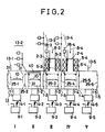
- An object of the embodiment is to fabricate a semiconductor layer with a p-i-n junction or an n-i-p junction by means of a multi-chamber system.
- the multi-chamber system as shown is comprised of five sections.
- the first section I is devoted to a loading chamber 1 ⁇ -1.
- the second section II is devoted to a second chamber 1 ⁇ -2, for example to deposit p-type layers.
- the third section III is devoted to a third chamber 1 ⁇ -3, for example to deposit i-type layers.
- the fourth section IV is devoted to a fourth chamber 1 ⁇ -4, for example to deposit n-type layers.
- the fifth section V is devoted to an unloading chamber 1 ⁇ -5. For fabrication of n-i-p junctions, the sections II and IV would be interchanged.
- Each chamber is provided with a doping system 13-1, 13-2,...13-5 and an evacuating system 11 comprising a turbo molecular pump 14-1, 14-2,... 14-5 and a vacuum pump 9-1, 9-2,...9-5.
- Each of the intermediate three chambers is formed with a reaction space 1-2, 1-3, 1-4 respectively.
- the second section II is a photo CVD system which is provided with a mercury lamp 40 and halogen lamps disposed in opposed relation relative to each other in a direction perpendicular to the plane of the drawing with the reaction chamber therebetween.
- the third and fourth sections are ECR enhanced CVD systems each of which is configured as in Fig.
- Argon gas may be employed as a resonating gas, as above described, but hydrogen gas may also be used in which case the magnitude of the magnetic field would have to be increased in inverse proportion to molecular weight.
- Gate valves 25-2, 25-3,...25-5 are disposed between adjacent chambers and the substrate holder 31 is arranged to be transported from one chamber to another through the respective gate valve when it is open. During deposition, of course, the valves are kept closed. The entrance valve 25-1 and the take-out valve 25-6 are, however, opened during deposition to enable new substrates to be loaded on to the holder in the loading chamber 1 ⁇ -1 via the entrance valve and to enable the substrate which has been deposited upon in the chambers 1 ⁇ -2, 1 ⁇ -3 and 1 ⁇ -4 to be removed.
- the deposition processes in the reaction spaces 1-3 and 1-4 might be carried out according to the particular methods above described.
- the supply of the productive gas and radiation of microwave energy are halted and the substrate holders 31 are transported by a transportation means (not shown in the figure) to the next adjacent chamber with the valves 25-1 and 25-6 closed.
- the transporting step is carried out swiftly without extracting the gaseous atmosphere inside each chamber.
- the resonating gas, argon gas may or may not be continuously introduced.
- the next deposition process is carried out respectively in the chambers 1 ⁇ -2, 1 ⁇ -3 and 1 ⁇ -4 with the valves 25-2 to 25-5 closed.
- a solar cell thus formed might have a conversion efficiency of 12.9%, an open circuit voltage of 0.92 V and a short circuit current density of 18.4 mV/cm2, with an effective area of 1.05 cm2.
- Such a high conversion efficiency is possibly attributed to the fact that no sputtering with the reactive gas takes place in the ECR/CVD system.
- the pressure in the chamber during deposition is only of the order of 1 x 10 ⁇ 3 to 1 x 10 ⁇ 5 torr, 3 x 10 ⁇ 4 torr for example, which is lower than that obtained in a glow discharge plasma system, enabling impurity gas and reactive gas to be exhausted by the turbo pump after deposition in a time which is reduced by a factor of 100 in comparison with the time required in a glow discharge CVD system.
- the gate valves 25-3 and 25-4 may be omitted from the system.
- buffer spaces might be provided between the respective chambers to improve the productivity of the system and the adjacent chambers might be substantially isolated by means of side walls of the holder 31.
- An exemplary solar cell fabricated according to this modification had a conversion efficiency of 12.6%, an open voltage of 0.93 V, a short current density of 18.3 mA/cm2 and a fill factor of 0.81, with its area of 1.05 cm2. Beside cost saving, it is made possible to transport the holder to the adjacent chamber within 5 minutes if the two valves 25-3 and 25-4 are dispensed with, thereby increasing the throughput of the system.
- the invention is also advantageous when applied to a process for manufacturing insulated-gate FETs of thin film type.
- the second section II is devoted to a reaction space in which is formed a semiconductor layer.
- the third section III is devoted to a reaction space in which is formed a silicon nitride layer.
- the fourth section IV is devoted to a reaction spaced in which is formed a silicon oxide layer.
- a glow discharge CVD system could be employed as a first section I in the embodiment of Fig. 2 instead of the photo enhanced CVD system.
- the present invention can be applied to light emitting MISs, super lattice light emitting devices and so on. As further applications, the invention is advantageous for other semiconductor lasers or optical integrated circuit devices.
- the ECR system in the embodiment is combined with a glow discharge CVD system
- a photo enhanced CVD system could instead be incorporated with the ECR system.
- an excimer laser having a wavelength of 100 to 400 nm, an argon laser, a nitrogen laser and so on might be used as a light source.
- disilane or a mixture of monosilane and Si2F6 may be used. This would be expected to improve the deposition speed even more.
- the substrate may be of silicon semiconductor, glass, synthetic resin, stainless steel or those which are provided with an electrode thereon.
- Si x Ge 1-x (0 ⁇ x ⁇ 1), Si x Sn 1-x (0 ⁇ x ⁇ 1), C x Ge 1-x (0 ⁇ x ⁇ 1), either i their intrinsic or impurity doped semiconductor states can be used.
- a substrate holder capable of holding a plurality of substrates as shown in Fig. 1 can be used for the multi-chamber system as shown n Fig. 2.
Landscapes
- Chemical & Material Sciences (AREA)
- Engineering & Computer Science (AREA)
- Physics & Mathematics (AREA)
- Plasma & Fusion (AREA)
- Organic Chemistry (AREA)
- General Chemical & Material Sciences (AREA)
- Chemical Kinetics & Catalysis (AREA)
- Materials Engineering (AREA)
- Mechanical Engineering (AREA)
- Metallurgy (AREA)
- Analytical Chemistry (AREA)
- Health & Medical Sciences (AREA)
- Electromagnetism (AREA)
- Toxicology (AREA)
- Photovoltaic Devices (AREA)
- Chemical Vapour Deposition (AREA)
Applications Claiming Priority (4)
| Application Number | Priority Date | Filing Date | Title |
|---|---|---|---|
| JP60253299A JP2654433B2 (ja) | 1985-11-12 | 1985-11-12 | 珪素半導体作製方法 |
| JP253299/85 | 1985-11-12 | ||
| JP259194/85 | 1985-11-18 | ||
| JP60259194A JPH0766911B2 (ja) | 1985-11-18 | 1985-11-18 | 被膜形成方法 |
Related Child Applications (1)
| Application Number | Title | Priority Date | Filing Date |
|---|---|---|---|
| EP91202023.7 Division-Into | 1991-08-06 |
Publications (3)
| Publication Number | Publication Date |
|---|---|
| EP0224360A2 true EP0224360A2 (de) | 1987-06-03 |
| EP0224360A3 EP0224360A3 (en) | 1987-08-19 |
| EP0224360B1 EP0224360B1 (de) | 1992-04-08 |
Family
ID=26541131
Family Applications (2)
| Application Number | Title | Priority Date | Filing Date |
|---|---|---|---|
| EP86308829A Expired - Lifetime EP0224360B1 (de) | 1985-11-12 | 1986-11-12 | Verfahren zur Herstellungeiner Halbleitervorrichtung |
| EP91202023A Withdrawn EP0457415A1 (de) | 1985-11-12 | 1986-11-12 | Verfahren zum Herstellen einer Halbleitervorrichtung |
Family Applications After (1)
| Application Number | Title | Priority Date | Filing Date |
|---|---|---|---|
| EP91202023A Withdrawn EP0457415A1 (de) | 1985-11-12 | 1986-11-12 | Verfahren zum Herstellen einer Halbleitervorrichtung |
Country Status (5)
| Country | Link |
|---|---|
| US (2) | US4808554A (de) |
| EP (2) | EP0224360B1 (de) |
| KR (3) | KR910003169B1 (de) |
| CN (3) | CN1029442C (de) |
| DE (1) | DE3684759D1 (de) |
Cited By (7)
| Publication number | Priority date | Publication date | Assignee | Title |
|---|---|---|---|---|
| GB2213835A (en) * | 1987-12-18 | 1989-08-23 | Gen Electric Co Plc | Deposition apparatus |
| EP0334109A1 (de) * | 1988-03-24 | 1989-09-27 | Siemens Aktiengesellschaft | Verfahren und Vorrichtung zum Herstellen von aus amorphen Silizium-Germanium-Legierungen bestehenden Halbleiterschichten nach der Glimmentladungstechnik, insbesondere für Solarzellen |
| WO1990010098A1 (en) * | 1989-02-24 | 1990-09-07 | Interuniversitair Micro-Elektronica Centrum Vzw | A method and an apparatus for disposing epitaxial silicon and silicides |
| EP0430079A3 (en) * | 1989-11-24 | 1992-03-18 | Nihon Shinku Gijutsu Kabushiki Kaisha | Chemical vapor deposition apparatus of in-line type |
| EP0497563A3 (en) * | 1991-01-29 | 1993-10-27 | Hitachi Ltd | Surface processing method using charged or not charged particles and apparatus for carrying out the same |
| FR2721754A1 (fr) * | 1994-03-25 | 1995-12-29 | Amoco Enron Solar | Procédé de dépôt par plasma pour améliorer les propriétés électriques et optiques de dispositifs photovoltaïques et électroniques et dispositifs obtenus. |
| EP0809283A3 (de) * | 1989-08-28 | 1998-02-25 | Hitachi, Ltd. | Verfahren zur Behandlung von Scheiben |
Families Citing this family (40)
| Publication number | Priority date | Publication date | Assignee | Title |
|---|---|---|---|---|
| US5780313A (en) * | 1985-02-14 | 1998-07-14 | Semiconductor Energy Laboratory Co., Ltd. | Method of fabricating semiconductor device |
| US6784033B1 (en) | 1984-02-15 | 2004-08-31 | Semiconductor Energy Laboratory Co., Ltd. | Method for the manufacture of an insulated gate field effect semiconductor device |
| US5753542A (en) | 1985-08-02 | 1998-05-19 | Semiconductor Energy Laboratory Co., Ltd. | Method for crystallizing semiconductor material without exposing it to air |
| US6673722B1 (en) | 1985-10-14 | 2004-01-06 | Semiconductor Energy Laboratory Co., Ltd. | Microwave enhanced CVD system under magnetic field |
| US6230650B1 (en) | 1985-10-14 | 2001-05-15 | Semiconductor Energy Laboratory Co., Ltd. | Microwave enhanced CVD system under magnetic field |
| KR910003742B1 (ko) * | 1986-09-09 | 1991-06-10 | 세미콘덕터 에너지 라보라터리 캄파니 리미티드 | Cvd장치 |
| US5258364A (en) * | 1987-10-07 | 1993-11-02 | Semiconductor Energy Laboratory Co., Ltd. | Method of shaping superconducting oxide material |
| US5179073A (en) * | 1987-10-07 | 1993-01-12 | Semiconductor Energy Laboratory Co., Ltd. | Method of shaping superconducting oxide material |
| JPH067594B2 (ja) * | 1987-11-20 | 1994-01-26 | 富士通株式会社 | 半導体基板の製造方法 |
| KR920003431B1 (ko) * | 1988-02-05 | 1992-05-01 | 가부시끼가이샤 한도다이 에네르기 겐뀨쇼 | 플라즈마 처리 방법 및 장치 |
| JPH01239919A (ja) * | 1988-03-22 | 1989-09-25 | Semiconductor Energy Lab Co Ltd | プラズマ処理方法およびプラズマ処理装置 |
| US5174881A (en) * | 1988-05-12 | 1992-12-29 | Mitsubishi Denki Kabushiki Kaisha | Apparatus for forming a thin film on surface of semiconductor substrate |
| US5407867A (en) * | 1988-05-12 | 1995-04-18 | Mitsubishki Denki Kabushiki Kaisha | Method of forming a thin film on surface of semiconductor substrate |
| US5232868A (en) * | 1988-10-04 | 1993-08-03 | Agency Of Industrial Science And Technology | Method for forming a thin semiconductor film |
| US5112776A (en) * | 1988-11-10 | 1992-05-12 | Applied Materials, Inc. | Method for planarizing an integrated circuit structure using low melting inorganic material and flowing while depositing |
| US4962063A (en) * | 1988-11-10 | 1990-10-09 | Applied Materials, Inc. | Multistep planarized chemical vapor deposition process with the use of low melting inorganic material for flowing while depositing |
| US5152866A (en) * | 1989-01-13 | 1992-10-06 | Hughes Aircraft Company | Plasma/radiation assisted molecular beam epitaxy method |
| DE69116058T2 (de) * | 1990-09-27 | 1996-08-22 | At & T Corp | Verfahren zur Herstellung integrierter Schaltungen |
| US5707692A (en) * | 1990-10-23 | 1998-01-13 | Canon Kabushiki Kaisha | Apparatus and method for processing a base substance using plasma and a magnetic field |
| TW237562B (de) * | 1990-11-09 | 1995-01-01 | Semiconductor Energy Res Co Ltd | |
| US5578520A (en) | 1991-05-28 | 1996-11-26 | Semiconductor Energy Laboratory Co., Ltd. | Method for annealing a semiconductor |
| US5766344A (en) * | 1991-09-21 | 1998-06-16 | Semiconductor Energy Laboratory Co., Ltd. | Method for forming a semiconductor |
| US6979840B1 (en) * | 1991-09-25 | 2005-12-27 | Semiconductor Energy Laboratory Co., Ltd. | Thin film transistors having anodized metal film between the gate wiring and drain wiring |
| US7097712B1 (en) * | 1992-12-04 | 2006-08-29 | Semiconductor Energy Laboratory Co., Ltd. | Apparatus for processing a semiconductor |
| CN100367461C (zh) * | 1993-11-05 | 2008-02-06 | 株式会社半导体能源研究所 | 一种制造薄膜晶体管和电子器件的方法 |
| US6897100B2 (en) * | 1993-11-05 | 2005-05-24 | Semiconductor Energy Laboratory Co., Ltd. | Method for processing semiconductor device apparatus for processing a semiconductor and apparatus for processing semiconductor device |
| JP3317209B2 (ja) * | 1997-08-12 | 2002-08-26 | 東京エレクトロンエイ・ティー株式会社 | プラズマ処理装置及びプラズマ処理方法 |
| AU5600200A (en) | 1999-06-10 | 2001-01-02 | Allied-Signal Inc. | Spin-on-glass anti-reflective coatings for photolithography |
| JP4439665B2 (ja) * | 2000-03-29 | 2010-03-24 | 株式会社半導体エネルギー研究所 | プラズマcvd装置 |
| GB0214273D0 (en) * | 2002-06-20 | 2002-07-31 | Boc Group Plc | Apparatus for controlling the pressure in a process chamber and method of operating same |
| DE102005004311A1 (de) * | 2005-01-31 | 2006-08-03 | Aixtron Ag | Verfahren und Vorrichtung zum Abscheiden von aus mehreren Komponentenhalbleitern bestehende Schichtenfolgen |
| US20090078199A1 (en) * | 2007-09-21 | 2009-03-26 | Innovation Vacuum Technology Co., Ltd. | Plasma enhanced chemical vapor deposition apparatus |
| US20110297088A1 (en) | 2010-06-04 | 2011-12-08 | Texas Instruments Incorporated | Thin edge carrier ring |
| CN104704624B (zh) * | 2012-10-09 | 2017-06-09 | 应用材料公司 | 具索引的串联基板处理工具 |
| US20150040970A1 (en) * | 2013-08-06 | 2015-02-12 | First Solar, Inc. | Vacuum Deposition System For Solar Cell Production And Method Of Manufacturing |
| CN103556126A (zh) * | 2013-10-14 | 2014-02-05 | 中国科学院半导体研究所 | 优化配置的多腔室mocvd反应系统 |
| US10544329B2 (en) | 2015-04-13 | 2020-01-28 | Honeywell International Inc. | Polysiloxane formulations and coatings for optoelectronic applications |
| KR20170005240A (ko) * | 2015-07-01 | 2017-01-12 | 주식회사 아바코 | 도전 산화물층의 증착 장비 및 방법 |
| CN109750274B (zh) * | 2017-11-01 | 2021-10-22 | 长鑫存储技术有限公司 | 半导体生产设备及半导体工艺方法 |
| CN111739971B (zh) | 2020-08-03 | 2021-02-19 | 苏州迈正科技有限公司 | 镀膜设备、方法、系统及太阳能电池、组件、发电系统 |
Family Cites Families (10)
| Publication number | Priority date | Publication date | Assignee | Title |
|---|---|---|---|---|
| US3594227A (en) * | 1968-07-12 | 1971-07-20 | Bell Telephone Labor Inc | Method for treating semiconductor slices with gases |
| CA1159012A (en) * | 1980-05-02 | 1983-12-20 | Seitaro Matsuo | Plasma deposition apparatus |
| JPS5766625A (en) * | 1980-10-11 | 1982-04-22 | Semiconductor Energy Lab Co Ltd | Manufacture of film |
| JPS58169980A (ja) * | 1982-03-19 | 1983-10-06 | Matsushita Electric Ind Co Ltd | 光起電力素子の製造方法 |
| US4435445A (en) * | 1982-05-13 | 1984-03-06 | Energy Conversion Devices, Inc. | Photo-assisted CVD |
| US4504518A (en) * | 1982-09-24 | 1985-03-12 | Energy Conversion Devices, Inc. | Method of making amorphous semiconductor alloys and devices using microwave energy |
| DE3375700D1 (en) * | 1982-10-12 | 1988-03-24 | Nat Res Dev | Infra red transparent optical components |
| US4515107A (en) * | 1982-11-12 | 1985-05-07 | Sovonics Solar Systems | Apparatus for the manufacture of photovoltaic devices |
| JPS59159167A (ja) * | 1983-03-01 | 1984-09-08 | Zenko Hirose | アモルフアスシリコン膜の形成方法 |
| JPS59200248A (ja) * | 1983-04-28 | 1984-11-13 | Canon Inc | 像形成部材の製造法 |
-
1986
- 1986-11-11 KR KR1019860009492A patent/KR910003169B1/ko not_active Expired
- 1986-11-12 EP EP86308829A patent/EP0224360B1/de not_active Expired - Lifetime
- 1986-11-12 CN CN86107683A patent/CN1029442C/zh not_active Expired - Lifetime
- 1986-11-12 EP EP91202023A patent/EP0457415A1/de not_active Withdrawn
- 1986-11-12 DE DE8686308829T patent/DE3684759D1/de not_active Expired - Lifetime
-
1987
- 1987-07-04 CN CN87104656.3A patent/CN1005881B/zh not_active Expired
- 1987-07-04 CN CN87104657A patent/CN1007565B/zh not_active Expired
- 1987-11-10 US US07/118,893 patent/US4808554A/en not_active Expired - Lifetime
- 1987-11-10 US US07/118,894 patent/US4808553A/en not_active Expired - Fee Related
-
1990
- 1990-07-27 KR KR1019900011462A patent/KR910003171B1/ko not_active Expired
- 1990-07-27 KR KR1019900011461A patent/KR910003170B1/ko not_active Expired
Cited By (11)
| Publication number | Priority date | Publication date | Assignee | Title |
|---|---|---|---|---|
| GB2213835A (en) * | 1987-12-18 | 1989-08-23 | Gen Electric Co Plc | Deposition apparatus |
| GB2213835B (en) * | 1987-12-18 | 1992-07-08 | Gen Electric Co Plc | Deposition apparatus |
| US5143018A (en) * | 1987-12-18 | 1992-09-01 | The General Electric Company, P.L.C. | Apparatus for depositing uniform films by how-pressure chemical vapor deposition |
| EP0334109A1 (de) * | 1988-03-24 | 1989-09-27 | Siemens Aktiengesellschaft | Verfahren und Vorrichtung zum Herstellen von aus amorphen Silizium-Germanium-Legierungen bestehenden Halbleiterschichten nach der Glimmentladungstechnik, insbesondere für Solarzellen |
| US4948750A (en) * | 1988-03-24 | 1990-08-14 | Siemens Aktiengesellschaft | Method and apparatus for producing semiconductor layers composed of amorphous silicon-germanium alloys through glow discharge technique, particularly for solar cells |
| WO1990010098A1 (en) * | 1989-02-24 | 1990-09-07 | Interuniversitair Micro-Elektronica Centrum Vzw | A method and an apparatus for disposing epitaxial silicon and silicides |
| EP0809283A3 (de) * | 1989-08-28 | 1998-02-25 | Hitachi, Ltd. | Verfahren zur Behandlung von Scheiben |
| EP0430079A3 (en) * | 1989-11-24 | 1992-03-18 | Nihon Shinku Gijutsu Kabushiki Kaisha | Chemical vapor deposition apparatus of in-line type |
| EP0497563A3 (en) * | 1991-01-29 | 1993-10-27 | Hitachi Ltd | Surface processing method using charged or not charged particles and apparatus for carrying out the same |
| US5462635A (en) * | 1991-01-29 | 1995-10-31 | Hitachi, Ltd. | Surface processing method and an apparatus for carrying out the same |
| FR2721754A1 (fr) * | 1994-03-25 | 1995-12-29 | Amoco Enron Solar | Procédé de dépôt par plasma pour améliorer les propriétés électriques et optiques de dispositifs photovoltaïques et électroniques et dispositifs obtenus. |
Also Published As
| Publication number | Publication date |
|---|---|
| EP0224360A3 (en) | 1987-08-19 |
| KR910003169B1 (ko) | 1991-05-20 |
| CN1007565B (zh) | 1990-04-11 |
| DE3684759D1 (de) | 1992-05-14 |
| US4808554A (en) | 1989-02-28 |
| CN1029442C (zh) | 1995-08-02 |
| KR920003833A (ko) | 1992-02-29 |
| KR870005438A (ko) | 1987-06-08 |
| US4808553A (en) | 1989-02-28 |
| KR920003832A (ko) | 1992-02-29 |
| KR910003170B1 (ko) | 1991-05-20 |
| CN87104657A (zh) | 1987-12-16 |
| CN1005881B (zh) | 1989-11-22 |
| EP0457415A1 (de) | 1991-11-21 |
| EP0224360B1 (de) | 1992-04-08 |
| KR910003171B1 (ko) | 1991-05-20 |
| CN87104656A (zh) | 1987-12-16 |
| CN86107683A (zh) | 1987-05-20 |
Similar Documents
| Publication | Publication Date | Title |
|---|---|---|
| EP0224360B1 (de) | Verfahren zur Herstellungeiner Halbleitervorrichtung | |
| US6113701A (en) | Semiconductor device, manufacturing method, and system | |
| US5512102A (en) | Microwave enhanced CVD system under magnetic field | |
| US6230650B1 (en) | Microwave enhanced CVD system under magnetic field | |
| US5397395A (en) | Method of continuously forming a large area functional deposited film by microwave PCVD and apparatus for the same | |
| EP0661760B1 (de) | Verfahren und Vorrichtung zur Bildung eines abgeschiedenen Films | |
| US4678679A (en) | Continuous deposition of activated process gases | |
| US4543267A (en) | Method of making a non-single-crystalline semi-conductor layer on a substrate | |
| US4988642A (en) | Semiconductor device, manufacturing method, and system | |
| US4760008A (en) | Electrophotographic photosensitive members and methods for manufacturing the same using microwave radiation in magnetic field | |
| US7588957B2 (en) | CVD process gas flow, pumping and/or boosting | |
| US6673722B1 (en) | Microwave enhanced CVD system under magnetic field | |
| KR920000591B1 (ko) | 마이크로파 강화 cvd시스템 | |
| JP2654433B2 (ja) | 珪素半導体作製方法 | |
| JP2564754B2 (ja) | 絶縁ゲイト型電界効果半導体装置の作製方法 | |
| JP3181121B2 (ja) | 堆積膜形成方法 | |
| JPH0766911B2 (ja) | 被膜形成方法 | |
| JP2890029B2 (ja) | 被膜形成装置及び被膜形成方法 | |
| JPH06216039A (ja) | マイクロ波プラズマcvd装置 | |
| JP3088703B2 (ja) | 薄膜型半導体装置の作製方法 | |
| JP2810531B2 (ja) | 堆積膜形成方法及び堆積膜形成装置 | |
| US4745000A (en) | Method of fabricating electrostatic drums using microwave energy | |
| JPH05304096A (ja) | 半導体装置作製方法 | |
| JPH05251356A (ja) | 被膜形成方法 | |
| JPH05190461A (ja) | 機能性堆積膜の連続形成方法および装置 |
Legal Events
| Date | Code | Title | Description |
|---|---|---|---|
| PUAI | Public reference made under article 153(3) epc to a published international application that has entered the european phase |
Free format text: ORIGINAL CODE: 0009012 |
|
| AK | Designated contracting states |
Kind code of ref document: A2 Designated state(s): DE FR GB |
|
| PUAL | Search report despatched |
Free format text: ORIGINAL CODE: 0009013 |
|
| RHK1 | Main classification (correction) |
Ipc: C23C 16/50 |
|
| AK | Designated contracting states |
Kind code of ref document: A3 Designated state(s): DE FR GB |
|
| 17P | Request for examination filed |
Effective date: 19880215 |
|
| 17Q | First examination report despatched |
Effective date: 19891010 |
|
| GRAA | (expected) grant |
Free format text: ORIGINAL CODE: 0009210 |
|
| AK | Designated contracting states |
Kind code of ref document: B1 Designated state(s): DE FR GB |
|
| XX | Miscellaneous (additional remarks) |
Free format text: TEILANMELDUNG 91202023.7 EINGEREICHT AM 12/11/86. |
|
| REF | Corresponds to: |
Ref document number: 3684759 Country of ref document: DE Date of ref document: 19920514 |
|
| ET | Fr: translation filed | ||
| PLBE | No opposition filed within time limit |
Free format text: ORIGINAL CODE: 0009261 |
|
| STAA | Information on the status of an ep patent application or granted ep patent |
Free format text: STATUS: NO OPPOSITION FILED WITHIN TIME LIMIT |
|
| 26N | No opposition filed | ||
| PGFP | Annual fee paid to national office [announced via postgrant information from national office to epo] |
Ref country code: GB Payment date: 19951103 Year of fee payment: 10 |
|
| PGFP | Annual fee paid to national office [announced via postgrant information from national office to epo] |
Ref country code: FR Payment date: 19951109 Year of fee payment: 10 |
|
| PGFP | Annual fee paid to national office [announced via postgrant information from national office to epo] |
Ref country code: DE Payment date: 19951113 Year of fee payment: 10 |
|
| PG25 | Lapsed in a contracting state [announced via postgrant information from national office to epo] |
Ref country code: GB Effective date: 19961112 |
|
| GBPC | Gb: european patent ceased through non-payment of renewal fee |
Effective date: 19961112 |
|
| PG25 | Lapsed in a contracting state [announced via postgrant information from national office to epo] |
Ref country code: FR Effective date: 19970731 |
|
| PG25 | Lapsed in a contracting state [announced via postgrant information from national office to epo] |
Ref country code: DE Effective date: 19970801 |
|
| REG | Reference to a national code |
Ref country code: FR Ref legal event code: ST |