EP0224968A2 - Dielektrische Passivierung - Google Patents
Dielektrische Passivierung Download PDFInfo
- Publication number
- EP0224968A2 EP0224968A2 EP86202124A EP86202124A EP0224968A2 EP 0224968 A2 EP0224968 A2 EP 0224968A2 EP 86202124 A EP86202124 A EP 86202124A EP 86202124 A EP86202124 A EP 86202124A EP 0224968 A2 EP0224968 A2 EP 0224968A2
- Authority
- EP
- European Patent Office
- Prior art keywords
- layer
- conductivity type
- passivating
- epitaxial
- semiconductor device
- Prior art date
- Legal status (The legal status is an assumption and is not a legal conclusion. Google has not performed a legal analysis and makes no representation as to the accuracy of the status listed.)
- Granted
Links
Images



Classifications
-
- H—ELECTRICITY
- H10—SEMICONDUCTOR DEVICES; ELECTRIC SOLID-STATE DEVICES NOT OTHERWISE PROVIDED FOR
- H10D—INORGANIC ELECTRIC SEMICONDUCTOR DEVICES
- H10D30/00—Field-effect transistors [FET]
- H10D30/60—Insulated-gate field-effect transistors [IGFET]
- H10D30/64—Double-diffused metal-oxide semiconductor [DMOS] FETs
- H10D30/65—Lateral DMOS [LDMOS] FETs
-
- H—ELECTRICITY
- H10—SEMICONDUCTOR DEVICES; ELECTRIC SOLID-STATE DEVICES NOT OTHERWISE PROVIDED FOR
- H10D—INORGANIC ELECTRIC SEMICONDUCTOR DEVICES
- H10D30/00—Field-effect transistors [FET]
- H10D30/60—Insulated-gate field-effect transistors [IGFET]
- H10D30/64—Double-diffused metal-oxide semiconductor [DMOS] FETs
-
- H—ELECTRICITY
- H10—SEMICONDUCTOR DEVICES; ELECTRIC SOLID-STATE DEVICES NOT OTHERWISE PROVIDED FOR
- H10D—INORGANIC ELECTRIC SEMICONDUCTOR DEVICES
- H10D64/00—Electrodes of devices having potential barriers
- H10D64/118—Electrodes comprising insulating layers having particular dielectric or electrostatic properties, e.g. having static charges
-
- H—ELECTRICITY
- H10—SEMICONDUCTOR DEVICES; ELECTRIC SOLID-STATE DEVICES NOT OTHERWISE PROVIDED FOR
- H10W—GENERIC PACKAGES, INTERCONNECTIONS, CONNECTORS OR OTHER CONSTRUCTIONAL DETAILS OF DEVICES COVERED BY CLASS H10
- H10W72/00—Interconnections or connectors in packages
- H10W72/90—Bond pads, in general
Definitions
- the present invention is directed to the provision of a stable high-voltage device which is less sensitive to the presence of both external and internal charges.
- Such a thick epitaxial layer 2 on the substrate 1 in Figure 1b may provide, for instance, a breakdown voltage of 370 volts.
- a reduction in surface field in the structure may be achieved when obtaining an ideal "RESURF * condition (constant electric field along nearly the complete device surface) as seen in Figure 1c.
- the breakdown voltage may then be increased to 1150 volts, with a nearly constant surface field.
- the present invention relates to a passivation scheme which not only shelters the device from external charges, but also alters the distribution of electric fields in the device to make it less vulnerable to the presence of internal charges. This tends to enhance the "RESURF” action by making the electric field distribution in the device even more constant and less sensitive to the effects of non-ideal geometries which occur in real devices.
- the present invention involves placing a layer of a very high dielectric constant material having a dielectric constant of at least ten times higher than that of silicon-dioxide, preferably of of at least 80 ( ⁇ ⁇ 80), over the insulating layer (normally an oxide layer).
- the present invention involves using a nonconductive dielectric material as an active passivation layer which shelters the device from electrical charges while also reducing the electric fields on its surface.
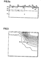
- This device includes a silicon substrate 11 of a first conductivity type, a buried layer 12 of the same conductivity type at the surface of the substrate 11, an epitaxial layer 13 of a second opposite conductivity type on the substrate 11 and buried layer 12, a surface layer 14 of the first conductivity type, and a surface layer 15 of the second conductivity type.
- Each of these layers may be appropriately doped layers of silicon.
- An insulating layer 16 of Si0 2 is provided over a portion of the surface of the epitaxial layer 13 and the surface layers 14 and 15.
- a layer 17 of high dielectric constant is provided as a passivation layer over a portion of both the epitaxial layer 13 and surface layer 15.
- An example of such a passivation layer 17 is titanium dioxide (Ti0 2 ) with a large static dielectric constant of approximately one order of magnitude larger than the dielectric constant of passivation materials commonly used such as silicon-dioxide.
- An electrode 18 of aluminium is provided at the surface of the device covering a small portion 19 of the edges of layer 17.
- Figure 3 provides a graphical illustration of the potential distribution in a lateral DMOST being made according to the prior art that has a passivation layer with a low dielectric constant value in comparison with the present invention.
- the electric equipotential contours 31 in Figure 3 (41 in Figure 4) have intervals of 20 volts.
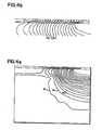
- Figure 4 modifies the potential distribution illustrated in Figure 3 by the introduction of the high dielectric constant passivation layer 17, such as shown in Figure 2.
- the effect of this high dielectric passivation layer becomes similar to that of an ohmic material although its origin is different. These materials are better suited layers under switching conditions and in addition will exhibit negligible gate to drain leakage.
- the electric equipotential contours 41 in Figure 4 are provided for a high-voltage lateral DMOST structure with a dielectric layer having a dielectric constant of approximately 80.
- the breakdown voltage in this case would be approximately 412 volts, whereas the breakdown voltage for the conventional structure illustrated in Figure 3 without the high dielectric constant passivating layer according to the present invention would be approximately 339 volts.
- the breakdown voltage is further illustrated as a function of the distance from the dielectric layer to the surface for a high-voltage lateral DMOST structure having passivating layers.
- the distance d from the dielectric layer 17 to the surface of the epitaxial layer 13 as illustrated in Figure 2b, is 0.1 micron, which is an optimum for the Ti0 2 passivation layer.
- the thickness of the passivation layer 17 is preferably 1 micron.
- Figure 5 illustrates the conditions of passivating layers of low dielectric constant of 3.9 (a) [prior artj, and high dielectric constants, such as 80 (b), 800 (c), and 8000 (d) [present invention].
- Figure 6 illustrates the breakdown voltage as a function of the static dieletric constant 9 of the passivating layer for a high-voltage lateral DMOST structure.
- Figure 7 illustrates the breakdown voltage as a function of the interface charge density Q ss for a high-voltage lateral DMOST structure having passivating layers of (a) low dielectric constant of the prior art of approximately 3.9, and (b) high dielectric constant of the present invention of about 80. This illustrates that the structure of Figure 2 would be much less sensitive to internal charges.
- Figures 5 and 6 emphasize that the more linear potential gradient according to the present invention results in a higher breakdown voltage with about a 20 % increase in breakdown voltage.
- the present invention is also applicable to other semiconductor devices, such as bi-polar transistors.
Landscapes
- Formation Of Insulating Films (AREA)
- Insulated Gate Type Field-Effect Transistor (AREA)
Applications Claiming Priority (2)
| Application Number | Priority Date | Filing Date | Title |
|---|---|---|---|
| US06/805,500 US4890150A (en) | 1985-12-05 | 1985-12-05 | Dielectric passivation |
| US805500 | 2001-03-13 |
Publications (3)
| Publication Number | Publication Date |
|---|---|
| EP0224968A2 true EP0224968A2 (de) | 1987-06-10 |
| EP0224968A3 EP0224968A3 (en) | 1989-05-03 |
| EP0224968B1 EP0224968B1 (de) | 1993-05-26 |
Family
ID=25191728
Family Applications (1)
| Application Number | Title | Priority Date | Filing Date |
|---|---|---|---|
| EP86202124A Expired - Lifetime EP0224968B1 (de) | 1985-12-05 | 1986-11-28 | Dielektrische Passivierung |
Country Status (5)
| Country | Link |
|---|---|
| US (1) | US4890150A (de) |
| EP (1) | EP0224968B1 (de) |
| JP (1) | JP2781175B2 (de) |
| CA (1) | CA1253261A (de) |
| DE (1) | DE3688500T2 (de) |
Cited By (1)
| Publication number | Priority date | Publication date | Assignee | Title |
|---|---|---|---|---|
| EP0519741A3 (en) * | 1991-06-21 | 1993-05-19 | Kabushiki Kaisha Toshiba | High-breakdown-voltage semiconductor element |
Families Citing this family (9)
| Publication number | Priority date | Publication date | Assignee | Title |
|---|---|---|---|---|
| SE0003360D0 (sv) * | 2000-09-21 | 2000-09-21 | Abb Ab | A semiconductor device |
| AU2003282909A1 (en) * | 2002-10-02 | 2004-04-23 | University Of Florida | Single chip radio with integrated antenna |
| DE102004007197B4 (de) | 2004-02-13 | 2012-11-08 | Infineon Technologies Ag | Hochsperrendes Halbleiterbauelement mit niedriger Durchlassspannung |
| DE102004007196A1 (de) * | 2004-02-13 | 2005-06-30 | Infineon Technologies Ag | Randabschluss für Halbleiterbauelement |
| TWI251922B (en) * | 2005-07-14 | 2006-03-21 | Siliconware Precision Industries Co Ltd | Multichip stack structure |
| WO2007139894A2 (en) | 2006-05-26 | 2007-12-06 | Cree Led Lighting Solutions, Inc. | Solid state light emitting device and method of making same |
| US7638811B2 (en) * | 2007-03-13 | 2009-12-29 | Cree, Inc. | Graded dielectric layer |
| DE202014004422U1 (de) | 2014-05-27 | 2014-06-13 | Infineon Technologies Ag | Bauteil mit Rand |
| US11081555B2 (en) * | 2018-06-27 | 2021-08-03 | Ohio State Innovation Foundation | Electronic devices with ultra-high dielectric constant passivation and high mobility materials |
Family Cites Families (12)
| Publication number | Priority date | Publication date | Assignee | Title |
|---|---|---|---|---|
| US3686544A (en) * | 1969-02-10 | 1972-08-22 | Philips Corp | Mosfet with dual dielectric of titanium dioxide on silicon dioxide to prevent surface current migration path |
| JPS52119082A (en) * | 1976-03-31 | 1977-10-06 | Mitsubishi Electric Corp | Low noise semiconductor unit |
| CA1131801A (en) * | 1978-01-18 | 1982-09-14 | Johannes A. Appels | Semiconductor device |
| US4300150A (en) * | 1980-06-16 | 1981-11-10 | North American Philips Corporation | Lateral double-diffused MOS transistor device |
| US4417325A (en) * | 1981-07-13 | 1983-11-22 | Eliyahou Harari | Highly scaleable dynamic ram cell with self-signal amplification |
| US4521446A (en) * | 1982-02-01 | 1985-06-04 | Texas Instruments Incorporated | Method for depositing polysilicon over TiO2 |
| US4494134A (en) * | 1982-07-01 | 1985-01-15 | General Electric Company | High voltage semiconductor devices comprising integral JFET |
| DE3480243D1 (en) * | 1983-03-31 | 1989-11-23 | Matsushita Electric Industrial Co Ltd | Method of manufacturing thin-film integrated devices |
| JPS60102770A (ja) * | 1983-11-09 | 1985-06-06 | Toshiba Corp | 半導体装置 |
| JPS60107854A (ja) * | 1983-11-16 | 1985-06-13 | Hitachi Ltd | キヤパシタ |
| US4639761A (en) * | 1983-12-16 | 1987-01-27 | North American Philips Corporation | Combined bipolar-field effect transistor resurf devices |
| US4609929A (en) * | 1984-12-21 | 1986-09-02 | North American Philips Corporation | Conductivity-enhanced combined lateral MOS/bipolar transistor |
-
1985
- 1985-12-05 US US06/805,500 patent/US4890150A/en not_active Expired - Lifetime
-
1986
- 1986-11-28 DE DE86202124T patent/DE3688500T2/de not_active Expired - Fee Related
- 1986-11-28 EP EP86202124A patent/EP0224968B1/de not_active Expired - Lifetime
- 1986-12-02 JP JP61286104A patent/JP2781175B2/ja not_active Expired - Fee Related
- 1986-12-04 CA CA000524582A patent/CA1253261A/en not_active Expired
Cited By (2)
| Publication number | Priority date | Publication date | Assignee | Title |
|---|---|---|---|---|
| EP0519741A3 (en) * | 1991-06-21 | 1993-05-19 | Kabushiki Kaisha Toshiba | High-breakdown-voltage semiconductor element |
| US5323041A (en) * | 1991-06-21 | 1994-06-21 | Kabushiki Kaisha Toshiba | High-breakdown-voltage semiconductor element |
Also Published As
| Publication number | Publication date |
|---|---|
| JP2781175B2 (ja) | 1998-07-30 |
| EP0224968A3 (en) | 1989-05-03 |
| US4890150A (en) | 1989-12-26 |
| DE3688500T2 (de) | 1993-12-09 |
| JPS62195133A (ja) | 1987-08-27 |
| EP0224968B1 (de) | 1993-05-26 |
| DE3688500D1 (de) | 1993-07-01 |
| CA1253261A (en) | 1989-04-25 |
Similar Documents
| Publication | Publication Date | Title |
|---|---|---|
| CA1131801A (en) | Semiconductor device | |
| Matsushita et al. | Highly reliable high-voltage transistors by use of the SIPOS process | |
| US5412241A (en) | Method for making an improved high voltage thin film transistor having a linear doping profile | |
| EP1208600B1 (de) | Hochspannungs-halbleiteranordnung mit einer feldplattenstruktur | |
| EP0182422B1 (de) | Halbleitervorrichtungen mit hoher Durchbruchspannung | |
| EP0620599B1 (de) | MOSFET mit niedrigdotiertem Drain und mit verbesserter Durchbruchspannungscharakteristik | |
| JP2812093B2 (ja) | プレーナ接合を有する半導体装置 | |
| EP0165644B1 (de) | Halbleiteranordnung mit Durchbruchspannung | |
| US4631562A (en) | Zener diode structure | |
| CA1227581A (en) | Semiconductor structure with resistive field shield | |
| CA1253261A (en) | Double layer dielectric passivation | |
| EP0181002A2 (de) | Halbleiterbauelement mit hoher Durchschlagspannung | |
| EP1038308B1 (de) | Laterale dünnschicht-soi-anordnung | |
| CA1121516A (en) | Power metal-oxide-semiconductor-field-effect- transistor | |
| KR100256387B1 (ko) | 수평 절연 게이트 반도체 장치 | |
| US5381031A (en) | Semiconductor device with reduced high voltage termination area and high breakdown voltage | |
| US6541804B2 (en) | Junction-isolated lateral MOSFET for high-/low-side switches | |
| US5323041A (en) | High-breakdown-voltage semiconductor element | |
| US6914270B2 (en) | IGBT with PN insulation and production method | |
| US3590343A (en) | Resonant gate transistor with fixed position electrically floating gate electrode in addition to resonant member | |
| KR20010102237A (ko) | 반도체 디바이스 | |
| EP0115098B1 (de) | Laterale DMOS-Transistoranordnung mit einer Injektionszone | |
| US4862242A (en) | Semiconductor wafer with an electrically-isolated semiconductor device | |
| US4430663A (en) | Prevention of surface channels in silicon semiconductor devices | |
| US6184565B1 (en) | Biasing of island-surrounding material to suppress reduction of breakdown voltage due to field plate acting on buried layer/island junction between high and low impurity concentration regions |
Legal Events
| Date | Code | Title | Description |
|---|---|---|---|
| PUAI | Public reference made under article 153(3) epc to a published international application that has entered the european phase |
Free format text: ORIGINAL CODE: 0009012 |
|
| AK | Designated contracting states |
Kind code of ref document: A2 Designated state(s): DE FR GB NL |
|
| PUAL | Search report despatched |
Free format text: ORIGINAL CODE: 0009013 |
|
| AK | Designated contracting states |
Kind code of ref document: A3 Designated state(s): DE FR GB NL |
|
| 17P | Request for examination filed |
Effective date: 19891101 |
|
| 17Q | First examination report despatched |
Effective date: 19910926 |
|
| GRAA | (expected) grant |
Free format text: ORIGINAL CODE: 0009210 |
|
| AK | Designated contracting states |
Kind code of ref document: B1 Designated state(s): DE FR GB NL |
|
| PG25 | Lapsed in a contracting state [announced via postgrant information from national office to epo] |
Ref country code: NL Effective date: 19930526 |
|
| REF | Corresponds to: |
Ref document number: 3688500 Country of ref document: DE Date of ref document: 19930701 |
|
| ET | Fr: translation filed | ||
| NLV1 | Nl: lapsed or annulled due to failure to fulfill the requirements of art. 29p and 29m of the patents act | ||
| PLBE | No opposition filed within time limit |
Free format text: ORIGINAL CODE: 0009261 |
|
| STAA | Information on the status of an ep patent application or granted ep patent |
Free format text: STATUS: NO OPPOSITION FILED WITHIN TIME LIMIT |
|
| 26N | No opposition filed | ||
| REG | Reference to a national code |
Ref country code: FR Ref legal event code: CD |
|
| PGFP | Annual fee paid to national office [announced via postgrant information from national office to epo] |
Ref country code: GB Payment date: 19971103 Year of fee payment: 12 |
|
| PGFP | Annual fee paid to national office [announced via postgrant information from national office to epo] |
Ref country code: FR Payment date: 19971118 Year of fee payment: 12 |
|
| PGFP | Annual fee paid to national office [announced via postgrant information from national office to epo] |
Ref country code: DE Payment date: 19980123 Year of fee payment: 12 |
|
| REG | Reference to a national code |
Ref country code: FR Ref legal event code: CD |
|
| PG25 | Lapsed in a contracting state [announced via postgrant information from national office to epo] |
Ref country code: GB Free format text: LAPSE BECAUSE OF NON-PAYMENT OF DUE FEES Effective date: 19981128 |
|
| GBPC | Gb: european patent ceased through non-payment of renewal fee |
Effective date: 19981128 |
|
| PG25 | Lapsed in a contracting state [announced via postgrant information from national office to epo] |
Ref country code: FR Free format text: LAPSE BECAUSE OF NON-PAYMENT OF DUE FEES Effective date: 19990730 |
|
| REG | Reference to a national code |
Ref country code: FR Ref legal event code: ST |
|
| PG25 | Lapsed in a contracting state [announced via postgrant information from national office to epo] |
Ref country code: DE Free format text: LAPSE BECAUSE OF NON-PAYMENT OF DUE FEES Effective date: 19990901 |