EP0225426B1 - Procédé pour fabriquer un transistor du type MOS sur un substrat - Google Patents
Procédé pour fabriquer un transistor du type MOS sur un substrat Download PDFInfo
- Publication number
- EP0225426B1 EP0225426B1 EP86108855A EP86108855A EP0225426B1 EP 0225426 B1 EP0225426 B1 EP 0225426B1 EP 86108855 A EP86108855 A EP 86108855A EP 86108855 A EP86108855 A EP 86108855A EP 0225426 B1 EP0225426 B1 EP 0225426B1
- Authority
- EP
- European Patent Office
- Prior art keywords
- gate electrode
- source
- oxide
- over
- substrate
- Prior art date
- Legal status (The legal status is an assumption and is not a legal conclusion. Google has not performed a legal analysis and makes no representation as to the accuracy of the status listed.)
- Expired - Lifetime
Links
Images


Classifications
-
- H—ELECTRICITY
- H10—SEMICONDUCTOR DEVICES; ELECTRIC SOLID-STATE DEVICES NOT OTHERWISE PROVIDED FOR
- H10P—GENERIC PROCESSES OR APPARATUS FOR THE MANUFACTURE OR TREATMENT OF DEVICES COVERED BY CLASS H10
- H10P30/00—Ion implantation into wafers, substrates or parts of devices
- H10P30/20—Ion implantation into wafers, substrates or parts of devices into semiconductor materials, e.g. for doping
- H10P30/202—Ion implantation into wafers, substrates or parts of devices into semiconductor materials, e.g. for doping characterised by the semiconductor materials
- H10P30/204—Ion implantation into wafers, substrates or parts of devices into semiconductor materials, e.g. for doping characterised by the semiconductor materials into Group IV semiconductors
-
- H—ELECTRICITY
- H10—SEMICONDUCTOR DEVICES; ELECTRIC SOLID-STATE DEVICES NOT OTHERWISE PROVIDED FOR
- H10D—INORGANIC ELECTRIC SEMICONDUCTOR DEVICES
- H10D30/00—Field-effect transistors [FET]
- H10D30/01—Manufacture or treatment
- H10D30/021—Manufacture or treatment of FETs having insulated gates [IGFET]
- H10D30/0223—Manufacture or treatment of FETs having insulated gates [IGFET] having source and drain regions or source and drain extensions self-aligned to sides of the gate
-
- H—ELECTRICITY
- H10—SEMICONDUCTOR DEVICES; ELECTRIC SOLID-STATE DEVICES NOT OTHERWISE PROVIDED FOR
- H10D—INORGANIC ELECTRIC SEMICONDUCTOR DEVICES
- H10D30/00—Field-effect transistors [FET]
- H10D30/60—Insulated-gate field-effect transistors [IGFET]
-
- H—ELECTRICITY
- H10—SEMICONDUCTOR DEVICES; ELECTRIC SOLID-STATE DEVICES NOT OTHERWISE PROVIDED FOR
- H10D—INORGANIC ELECTRIC SEMICONDUCTOR DEVICES
- H10D62/00—Semiconductor bodies, or regions thereof, of devices having potential barriers
- H10D62/10—Shapes, relative sizes or dispositions of the regions of the semiconductor bodies; Shapes of the semiconductor bodies
- H10D62/13—Semiconductor regions connected to electrodes carrying current to be rectified, amplified or switched, e.g. source or drain regions
- H10D62/149—Source or drain regions of field-effect devices
- H10D62/151—Source or drain regions of field-effect devices of IGFETs
-
- H—ELECTRICITY
- H10—SEMICONDUCTOR DEVICES; ELECTRIC SOLID-STATE DEVICES NOT OTHERWISE PROVIDED FOR
- H10P—GENERIC PROCESSES OR APPARATUS FOR THE MANUFACTURE OR TREATMENT OF DEVICES COVERED BY CLASS H10
- H10P30/00—Ion implantation into wafers, substrates or parts of devices
- H10P30/20—Ion implantation into wafers, substrates or parts of devices into semiconductor materials, e.g. for doping
- H10P30/208—Ion implantation into wafers, substrates or parts of devices into semiconductor materials, e.g. for doping of electrically inactive species
-
- H—ELECTRICITY
- H10—SEMICONDUCTOR DEVICES; ELECTRIC SOLID-STATE DEVICES NOT OTHERWISE PROVIDED FOR
- H10P—GENERIC PROCESSES OR APPARATUS FOR THE MANUFACTURE OR TREATMENT OF DEVICES COVERED BY CLASS H10
- H10P30/00—Ion implantation into wafers, substrates or parts of devices
- H10P30/20—Ion implantation into wafers, substrates or parts of devices into semiconductor materials, e.g. for doping
- H10P30/21—Ion implantation into wafers, substrates or parts of devices into semiconductor materials, e.g. for doping of electrically active species
- H10P30/212—Through-implantation
-
- H—ELECTRICITY
- H10—SEMICONDUCTOR DEVICES; ELECTRIC SOLID-STATE DEVICES NOT OTHERWISE PROVIDED FOR
- H10P—GENERIC PROCESSES OR APPARATUS FOR THE MANUFACTURE OR TREATMENT OF DEVICES COVERED BY CLASS H10
- H10P76/00—Manufacture or treatment of masks on semiconductor bodies, e.g. by lithography or photolithography
- H10P76/40—Manufacture or treatment of masks on semiconductor bodies, e.g. by lithography or photolithography of masks comprising inorganic materials
- H10P76/408—Manufacture or treatment of masks on semiconductor bodies, e.g. by lithography or photolithography of masks comprising inorganic materials characterised by their sizes, orientations, dispositions, behaviours or shapes
- H10P76/4085—Manufacture or treatment of masks on semiconductor bodies, e.g. by lithography or photolithography of masks comprising inorganic materials characterised by their sizes, orientations, dispositions, behaviours or shapes characterised by the processes involved to create the masks
Definitions
- This invention relates to a method of fabricating a MOS transistor on a substrate. It is particularly directed to improved processing techniques for fabricating MOS (metal oxide semiconductor) transistors in a large scale integrated circuit.
- a MOS transistor generally includes source/drain regions in a substrate, and a gate electrode formed above the substrate between the source/drain regions and separated from the substrate by a relatively thin dielectric.
- the relative alignment of the gate with its source/drain regions is an important factor which influences the performance of the transistor.
- IBM Technical Disclosure Bulletin, Volume 24, No. 7A December 1981, pages 3417-3419 shows a technique for fabricating a MOS transistor in which an implant mask on the sides of the gate electrode shields an underlying portion of the substrate from implantation so that initially there is a gap between the side edge of the gate electrode and a side edge of the implanted region.
- GB-A-2074374A discloses a technique for fabricating an MOS transistor in which a layer of insulating oxide is put down over the substrate, a layer of polysilicon is then deposited followed by a further layer of oxide. The polysilicon and further oxide layer are then etched to define a gate electrode with an oxide cap. A separate oxide layer is then grown which forms an implant mask on the side wall of the gate and augments the thickness of the oxide cap.
- US-A-4210993 discloses a technique for fabricating an MOS transistor in which a gate is defined by etching from a layer of polysilicon placed on a semiconductor substrate with an intervening layer of gate oxide. A silicon dioxide film is grown by thermal oxidation so that the oxide layer produced on the surface of the gate is thicker than the oxide film produced on the substrate. The oxide layer on the sides of the gate then acts as an implant mask.
- EP-A-0072967 forming part of the state of the art under Article 54(3) of the European Patent Convention, and in which an oxide layer formed over the gate acts as an implant mask for forming the source and drain regions.
- This oxide layer is grown by thermal oxidation so that the oxide layer produced on the surface of the gate is thicker than the oxide film over the source and drain regions.
- a method of fabricating on a substrate a MOS transistor having a gate electrode and a self-aligned source/drain region comprising the steps of:
- a method of fabricating on a substrate a MOS transistor having a gate electrode and a pair of source/drain regions comprising forming a relatively thin gate insulator over the substrate and over the intended source/drain regions defining a polysilicon gate electrode over the gate insulator between the intended source/drain regions, establishing a dielectric layer over the gate electrode and the gate insulator such that the dielectric is relatively thick at least over the sides of the gate electrode and relatively thinner over the intended source/drain regions and implanting the source/drain regions such that they are laterally offset from the substrate area below the gate electrode by the thickness of the dielectric layer on the sides of the gate electrode characterised by before the step of establishing a dielectric layer over the gate electrode, nitrogen is implanted while protecting the gate electrode from the implant and by heat driving the source/drain regions laterally until their edges are substantially vertically aligned with the sides of the gate electrode, etching contact areas so as to lay bare the substrate holding the source/d
- a method for controlling the alignment of the source/drain regions of a typical MOS transistor with its polysilicon gate electrode, and for forming self-aligned source/drain contacts. Thereafter, alternate techniques are described for achieving the same result in applications where polysilicon or other gate materials are used, and which provide control over various other aspects of fabrication. As described more specifically below, the self-aligned source/drain regions are formed even into bare silicon, if desired, while simultaneously providing an isolating layer of dielectric, for example, on the gate of the transistor.
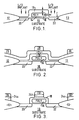
- FIG. 1 there is shown a substrate 10 and field oxide regions 12 and 13 which are formed in a conventional manner, such as by local oxidation. Between these field oxide regions, an MOS transistor is fabricated by first forming a gate oxide 14 in the usual manner. Next, a polysilicon layer, designated Poly and doped to a sheet resistance of about 20 ohms per square, is defined and etched using photoresist patterning techniques. This leaves a Poly gate electrode 16 disposed above the transistor's intended channel.
- Poly polysilicon layer
- a dielectric layer 18 of oxide is then established on the top and sides of the gate electrode 16 and over the substrate adjacent the gate electrode such that the oxide layer on the top and sides of the gate electrode is relatively thick compared to the oxide layer adjacent the gate electrode over the intended source/drain regions.
- This is preferably acomplished by steam oxidation at 850°C until about 500 nanometres of the oxide 18 are provided over the top (dimension A) of the gate electrode.
- This step of differentially growing the oxide provides a substantially similar oxide thickness on the side (dimension B) of the gate electrode and a relatively thin oxide layer (dimension C) over the intended source/drain regions. This thickness of the oxide layer at C will typically be about 170 nanometres because the oxide grows faster over the top and sides of the doped gate electrode.
- the thickness of the oxide on the sides of the gate electrode (dimension B) is chosen so that later implanted sources and drains will be closely aligned with the vertical edges of the gate electrode 16 at the conclusion of transistor fabrication without any substantial gap or overlap between the source/drain regions and the gate electrode. That is, the oxide on the sides of the gate electrode acts as an implant mask to shield underlying portions of the substrate from implantation.
- source/drain regions are implanted with arsenic or phosphorus, for example, to a depth which may be about 0.3 micron at a dose of about 6 x 10¹⁵ ions per square centimetre. Because of the masking effect provided by the oxide on the sides of the gate electrode 16, the source/drain regions 20 and 22 are not implanted adjacent the vertical edges of the gate electrode. Rather, a gap is provided between the gate electrode 16 and the source/drain regions to allow for subsequent diffusion of the source/drain regions.
- an anisotropic etch is used to remove or thin the oxide layers which overlie the source/drain regions.
- the anisotropic etch may be a plasma etch as described below.
- the anisotropy of the etch may be desirable to modify the anisotropy of the etch to controllably thin the oxide on the sidewall of the gate electrode to provide a smaller gap, 300 nanometres for example, where subsequent heat treatments are known to provide less lateral diffusion of the source/drain regions.
- the implanted source/drain regions After the source/drain regions have been implanted, standard processing occurs, including heat treating the structure. During such heat treatment, the implanted source/drain regions are driven deeper (to about 0.7 micrometre, for example) and driven laterally into substantial alignment with the vertical edges of the gate electrode ( Figure 2). Good alignment is achieved by establishing the thickness of the oxide layer 18 on the sides of the gate electrode so that the known heat treatments which follow cause the edges of the source/drain regions to be driven laterally by a distance which is substantially equal to dimension B.
- a nitrogen implant is used prior to forming the oxide layer 18 (Figure 1) to reduce the rate of oxidation over the source/drain regions while not affecting the rate of oxidation on Poly.
- the gate electrode is protected from the implant by a photoresist layer.
- Source/drain implants may then be done after the oxide layer 18 is formed, and source/drain drive-in can be tailored to prevent overlap between the Poly gate electrode and the source/drain regions.
- an intermediate oxide layer 24 is deposited to a depth of about 500 nanometres, for example. As shown in Figure 2, this intermediate oxide layer preferably covers the entire structure, including the field oxide regions 12 and 13.
- Contact regions for the gate electrode and the source/drain regions are established by pattern-defining a photoresist layer at 26, 28 and 30. As shown, a contact region is thus formed between photoresists 26 and 28. This contact region overlaps the field oxide region 12 and the gate electrode. A similar overlap is created in the are between photoresists 28 and 30.
- the oxide layers 18 and 24 are removed from the contact areas so that the substrate is exposed above the source/drain regions, preferably by using a plasma etch.
- the field oxide not masked by photoresist is also laid bare, and the unmasked oxide layer 18 which overlies the gate electrode may be thinned.
- Such a plasma etch may, for example, be carried out in a reactive plasma etcher capable of anisotropic etching.
- a parallel plate reactor with close spacing (about 2 centimetres) between the plates is effective using 50% CHF3 and 50% C2F6 at a total pressure of about 93.1 Pa (700 millitorrs) and a power of about 2000 watts.
- the dielectric layers 18 and 24 may be made of either similar materials or different materials. It may be desired to use different material to provide an etch stop which avoids thinning dielectric 18 over the gate electrode.
- dielectrics 18 and 24 are of a similar material such as silicon dioxide
- a thin layer of another dielectric such as a nitride may be deposited on the dielectric 18 prior to forming the dielectric 24. This also prevents the etching from removing the oxide 18 whilst the dielectric 24 is being removed. In any case, and oxide layer 18 will remain on the gate electrode 16 to facilitate the formation of self-aligned contacts or interconnnects for the source/drain regions.
- the directional etching described above provides the structure shown in Figure 3 in which an intermediate oxide layer 24a and a photoresist 26 are left over the illustrated portion of the field oxide 12.
- the illustrated portion of the field oxide 13 is covered by an intermediate oxide layer 24c and photoresist 30, and the central portion of the remaining oxide layer is covered by an intermediate oxide layer 24b and photoresist 28.
- interconnect contacting layer 32, 34 such as aluminium or polysilicon
- interconnect 32 overlies the source/drain region 20 and overlaps both the Poly gate and the field oxide 12.
- interconnnect 34 overlies the source/drain region 22 and overlaps both the Poly gate and the field oxide region 13.
- the fabrication tehnique described above has several advantages. Chief among thse is the lack of undesired overlap between the finally processed source/drain regions and the Poly gate. Consequently, the transistor has reduced Miller capacitance and, therefore, operates faster. In addition, the width of the Poly gate is substantially equal to the transistor's electrical channel length. This allows transistors with longer channel characteristics to be fabricated with smaller physical dimensions.
- the source/drain contacts can be self-aligning. This result is obtained because the technique allows etching to the substrate over the source/drain regions while the oxide layer 18 protects the Poly gate. Even if the photoresist 28 is misaligned with respect to the gate 16, the oxide 18 prevents shorts to the gate when the interconnects 32, 34 are provided for the source/drain regions.
- the manner in which the interconnects are provided also contributes substantially to a reduction in transistor size.
- the interconnect patterns 32 and 34 overlap the Poly 16 while covering the active areas designated by the shaded regions 36 and 38.
- the Poly and the active areas are about 2 microns wide, and an overlap of about .5 micrometre (dimension D) exists between the interconnect patterns and the Poly. Consequently, the size (dimension E) of the transistor is reduced to about 7 microns or less.
- the use of the intermediate oxide layer 24 may be eliminated and contact areas may be defined by a non-selective etch.
- the resulting structure would be substantially as shown in Figure 4, except that the intermediate oxide would not be present. This technique is useful in forming self-aligned buried contacts.
- the method described with reference to Figures 1-4 utilizes the differential growth rate of dielectric over the gate electrode and over the source/drain regions to provide self-aligned, non-overlapping source/drain regions.
- Figures 6 and 7 show a method which may be used when it is desired to dope the polysilicon gate at the same time as the source/drain regions are doped.
- a dielectric 14b is established over the substrate 10b and then a polysilicon gate 16b is defined over the dielectric 14b.
- Another dielectric 46 such as silicon dioxide, is then deposited or grown over the entire structure. The dielectric 46 is anisotropically etched, as by the previously described plasma etch, to expose the bare silicon substrate and the top of the gate electrode 16b as shown in Figure 7.
- FIG. 8 This variant is shown in Figure 8 in which an oxide layer 48, having a thickness typically less than 100 nanometres, is grown or deposited over the gate 16b, over the remanants 46a and 46b (not shown separately in Figure 8), and over the substrate.
- Source/drain regions 20b and 22b may then be implanted through the oxide layer 48 while the gate electrode 16b is simultaneously doped.
- the remnants on the sides of the gate electrode, as shown in Figure 7 may be formed of material other than dielectric.
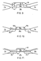
- One such material is photoresist, and it may be utilized as described in connection with Figures 9 and 10.
- a dielectric 14c is established over the substrate 10c in the usual manner, and a gate electrode 16c of polysilicon, for example, is defined over the intended channel of the transistor.
- a layer of photoresist material 50 is then conformally established in a conventional manner over the entire structure. This results in a layer of photoresist having a depth H over the intended source/drain regions and over the gate electrode 16c. A greater depth I of photoresist occurs in the areas adjacent the sides of the gate electrode.
- photoresist is then exposed and developed conventionally or anisotropically etched so as to remove a thickness H of it. Because of the greater depth of the photoresist at the areas adjacent the gate electrode, photoresist remnants or fillets 50a and 50b ( Figure 13) remain on the sides of the gate electrode. These fillets serve, of course, to mask the source/drain implantation as described in the other examples.
- the source/drain regions 20c and 22c may now be implanted. Because the gate electrode 16 is uncovered, this implantation also dopes the gate electrode.
- the photoresist fillets 50a and 50b are stripped conventionally. Then an oxide layer 52 ( Figure 11) may be established over the entire structure. Preferably, about 50 nanometres of the oxide 52 are grown thermally and the remainder is deposited. Next, the previously described processing occcurs, including the heat treatment which drives the source/drain regions 20c and 22c into the depicted non-overlapping alignment with the vertical edges of the gate electrode 16c.
- a layer of oxide may be deposited over the gate material prior to the application of the photoresist.
- the gate material and oxide may then be defined to form a gate electrode in which an oxide is on top of the gate electrode material.
- the photoresist may then be applied and selectively removed as previously described, with the result that an oxide layer 54 ( Figure 9) separates the photoresist from the top of the gate electrode. This oxide layer prevents the gate material from being doped during source/drain implantation.
- all such methods provide an implant mask which ensures that the source/drain regions are properly aligned with the gate electrode at the conclusion of fabrication.
- the implant mask serves to isolate the gate electrode, particularly its edges, from interconnects so that the patterns which define the interconnects need not be held to tight tolerances.
Landscapes
- Insulated Gate Type Field-Effect Transistor (AREA)
- Electrodes Of Semiconductors (AREA)
Claims (9)
- Procédé de fabrication sur un substrat, d'un transistor MOS ayant une électrode de grille et une région de source/drain auto-alignée, le procédé comprenant les étape de :a) formation d'une électrode de grille (16) de silicium polycristallin dopé sur le substrat (10) mais isolé de celui-ci ;b) ensuite croissance thermique différentielle d'un oxyde (18) jusqu'à une épaisseur commandée sur le dessus et les côtés de l'électrode de grille (16) et sur le substrat (10) adjacent à l'électrode de grille, l'oxyde sur le dessus et les côtés de l'électrode de grille étant relativement épais par comparaison à l'oxyde sur une région du substrat destinée à être la région de source/drain ;c) ensuite gravure anisotrope dudit oxyde (18) de manière à ce que ledit oxyde définisse un masque d'implantation sur les côtés de l'électrode de grille (16) ; etd) implantation d'au moins une région de source/drain (20, 22) dans le substrat (10) de manière à ce que le masque d'implantation (18) protège de l'implantation une partie sous-jacente du substrat (10) pour fournir un écart entre un bord latéral de l'électrode de grille et un bord latéral de la région implantée, comprenant en outre l'étape d'implantation d'azote, avant l'étape b), tout en protégeant l'électrode de grille de l'implantation ; et l'étape de pilotage par la chaleur de la région de source/drain (20, 22) implantée jusqu'à ce que son bord latéral soit sensiblement aligné avec le bord latéral antérieurement séparé de l'électrode de grille (16), dans lequel la largeur de l'oxyde sur les côtés de l'électrode de grille est commandée dans l'étape b) de manière à ce que l'étape de pilotage par la chaleur fasse que le bord de la source/drain soit sensiblement aligné avec le bord de l'électrode de grille avec un chevauchement sensiblement nul.
- Procédé tel que revendiqué dans la revendication 1, dans lequel l'oxyde est développé par croissance en phase vapeur à une température d'environ 850° C.
- Procédé tel que revendiqué dans la revendication 1 ou la revendication 2, dans lequel la région de source/drain (20, 22) est implantée à travers la couche d'oxyde relativement mince sur le substrat.
- Procédé tel que revendiqué dans la revendication 1 ou la revendication 2, dans lequel ladite étape de gravure anisotrope retire l'oxyde (18) sur la région destinée à être la région de source/drain (20, 22) et laisse masqué l'oxyde (B) sur les côtés de l'électrode de grille (16).
- Procédé tel que revendiqué dans l'une quelconque des revendications précédentes, comprenant de plus, après ladite étape d'implantation d), la formation d'un diélectrique intermédiaire (24) sur à la fois l'électrode de grille (16) et la région de source/drain (20, 22), le dessin d'une zone de contact sur la région de source/drain (20, 22) pour recouvrir la région de source/drain et chevaucher l'oxyde sur l'électrode de grille (16), la gravure du diélectrique (24) dans la zone de contact jusqu'à la surface (10) tout en laissant l'oxyde (18) sur les côtés et le dessus de l'électrode de grille (16), et la mise en place d'un matériau conducteur (32, 34) dans la zone de contact gravée pour réaliser un contact pour la région de source/drain (20, 22), ce par quoi un contact auto-aligné est formé de manière à ce que l'électrode de grille (16) soit empêchée par l'oxyde (18) sur l'électrode de grille d'être raccourcie dans le cas où la zone de contact dessinée serait mal alignée.
- Procédé tel que revendiqué dans l'une quelconque des revendications précédentes, dans lequel ladite électrode de grille (16) est du silicium polycristallin dopé jusqu'à une résistance de couche d'environ 20 ohms par carré.
- Procédé tel que revendiqué dans l'une quelconque des revendications précédentes, dans lequel l'oxyde est gravé de manière anisotrope pour laisser de l'oxyde sur au moins les côtés de ladite électrode de grille (16b), et dans lequel la région de source/drain (20b, 22b) est implantée tandis que le dessus de l'électrode de grille (16b) est pratiquement exempt d'oxyde pour le dopage de l'électrode de grille (16b) pendant l'implantation de la source/drain.
- Procédé tel que revendiqué dans la revendication 7, dans lequel un oxyde relativement mince (48) est formé sur l'électrode de grille (16b), les restes d'oxyde (46a, 46b) sur les côtés de l'électrode de grille, et la région destinée à être la région de source/drain (22a, 22b) avant l'implantation.
- Procédé de fabrication sur un substrat d'un transistor MOS ayant une électrode de grille et une paire de régions de source/drain, comprenant la formation d'un isolant de grille (14) relativement mince sur le substrat (10) et sur les régions destinées à être les régions de source/drain (20, 22) en définissant une électrode de grille (16) de silicium polycristallin sur l'isolant de grille (14) entre les régions destinées à être les régions de source/drain (20, 22), l'établissement d'une couche diélectrique (18) sur l'électrode de grille (16) et l'isolant de grille (14) de manière à ce que le diélectrique (18) soit relativement épais au moins sur les côtés de l'électrode de grille (16) et relativement plus mince sur les régions destinées à être les régions de source/drain (20, 22), et implantation des régions de source/drain de manière à ce qu'elles soient décalées latéralement, par rapport à la surface du substrat située sous l'électrode de grille (16), de l'épaisseur de la couche diélectrique (18) située sur les côtés de l'électrode de grille (16), comprenant en outre l'étape d'implantation d' azote, avant l'étape d'établissement d'une couche diélectrique sur l'électrode de grille, tout en protégeant l'électrode de grille de l'implantation, et l'étape de pilotage par la chaleur des régions de source/drain (20, 22), latéralement, jusqu'à ce que leurs bords soient sensiblement alignés verticalement avec les côtés de l'électrode de grille (16), la gravure de zones de contact de manière à mettre à nu le substrat (10) contenant les régions source/drain (20, 22) et à conserver le diélectrique (18) sur les côtés de l'électrode de grille (16), et la formation de contacts conducteurs (32, 34) dans les zones gravées, ce par quoi les régions de source/drain (20, 22) sont correctement alignées avec l'électrode de grille (16) et les contacts métalliques (32, 34) sont alignés avec les régions de source/drain (20, 22) sans raccourcissement de l'électrode de grille (16).
Applications Claiming Priority (2)
| Application Number | Priority Date | Filing Date | Title |
|---|---|---|---|
| US33147481A | 1981-12-16 | 1981-12-16 | |
| US331474 | 1981-12-16 |
Related Parent Applications (1)
| Application Number | Title | Priority Date | Filing Date |
|---|---|---|---|
| EP82306614.7 Division | 1982-12-10 |
Publications (3)
| Publication Number | Publication Date |
|---|---|
| EP0225426A2 EP0225426A2 (fr) | 1987-06-16 |
| EP0225426A3 EP0225426A3 (en) | 1987-10-28 |
| EP0225426B1 true EP0225426B1 (fr) | 1992-11-11 |
Family
ID=23294125
Family Applications (2)
| Application Number | Title | Priority Date | Filing Date |
|---|---|---|---|
| EP82306614A Expired EP0081999B1 (fr) | 1981-12-16 | 1982-12-10 | Procédé pour la fabrication d'un transistor MOS sur un substrat |
| EP86108855A Expired - Lifetime EP0225426B1 (fr) | 1981-12-16 | 1982-12-10 | Procédé pour fabriquer un transistor du type MOS sur un substrat |
Family Applications Before (1)
| Application Number | Title | Priority Date | Filing Date |
|---|---|---|---|
| EP82306614A Expired EP0081999B1 (fr) | 1981-12-16 | 1982-12-10 | Procédé pour la fabrication d'un transistor MOS sur un substrat |
Country Status (4)
| Country | Link |
|---|---|
| EP (2) | EP0081999B1 (fr) |
| JP (1) | JPH0640549B2 (fr) |
| CA (1) | CA1197926A (fr) |
| DE (2) | DE3279079D1 (fr) |
Families Citing this family (6)
| Publication number | Priority date | Publication date | Assignee | Title |
|---|---|---|---|---|
| US4603472A (en) * | 1984-04-19 | 1986-08-05 | Siemens Aktiengesellschaft | Method of making MOS FETs using silicate glass layer as gate edge masking for ion implantation |
| JPS61117868A (ja) * | 1984-11-14 | 1986-06-05 | Toshiba Corp | 半導体装置及びその製造方法 |
| KR960001611B1 (ko) | 1991-03-06 | 1996-02-02 | 가부시끼가이샤 한도다이 에네르기 겐뀨쇼 | 절연 게이트형 전계 효과 반도체 장치 및 그 제작방법 |
| EP0549055A3 (en) * | 1991-12-23 | 1996-10-23 | Koninkl Philips Electronics Nv | Method of manufacturing a semiconductor device provided with a field effect transistor, and such a semiconductor device |
| US6624450B1 (en) | 1992-03-27 | 2003-09-23 | Semiconductor Energy Laboratory Co., Ltd. | Semiconductor device and method for forming the same |
| CN110223990B (zh) * | 2019-06-18 | 2022-03-08 | 京东方科技集团股份有限公司 | 顶栅结构及其制备方法、阵列基板、显示设备 |
Family Cites Families (8)
| Publication number | Priority date | Publication date | Assignee | Title |
|---|---|---|---|---|
| NL161305C (nl) * | 1971-11-20 | 1980-01-15 | Philips Nv | Werkwijze voor het vervaardigen van een halfgeleiderin- richting. |
| JPS5235983A (en) * | 1975-09-17 | 1977-03-18 | Hitachi Ltd | Manufacturing method of field effective transistor |
| JPS52130567A (en) * | 1976-04-26 | 1977-11-01 | Toshiba Corp | Preparation of semiconductor device |
| JPS5444482A (en) * | 1977-09-14 | 1979-04-07 | Matsushita Electric Ind Co Ltd | Mos type semiconductor device and its manufacture |
| US4182023A (en) * | 1977-10-21 | 1980-01-08 | Ncr Corporation | Process for minimum overlap silicon gate devices |
| JPS5476069A (en) * | 1977-11-30 | 1979-06-18 | Fujitsu Ltd | Manufacture of semiconductor device |
| US4287661A (en) * | 1980-03-26 | 1981-09-08 | International Business Machines Corporation | Method for making an improved polysilicon conductor structure utilizing reactive-ion etching and thermal oxidation |
| FR2481005A1 (fr) * | 1980-04-17 | 1981-10-23 | Western Electric Co | Procede de fabrication de transistors a effet de champ a canal court |
-
1982
- 1982-11-30 CA CA000416638A patent/CA1197926A/fr not_active Expired
- 1982-12-10 DE DE8282306614T patent/DE3279079D1/de not_active Expired
- 1982-12-10 EP EP82306614A patent/EP0081999B1/fr not_active Expired
- 1982-12-10 EP EP86108855A patent/EP0225426B1/fr not_active Expired - Lifetime
- 1982-12-10 DE DE8686108855T patent/DE3280420T2/de not_active Expired - Lifetime
- 1982-12-16 JP JP57221086A patent/JPH0640549B2/ja not_active Expired - Lifetime
Also Published As
| Publication number | Publication date |
|---|---|
| EP0225426A2 (fr) | 1987-06-16 |
| JPS58147071A (ja) | 1983-09-01 |
| CA1197926A (fr) | 1985-12-10 |
| JPH0640549B2 (ja) | 1994-05-25 |
| EP0081999B1 (fr) | 1988-09-28 |
| EP0081999A2 (fr) | 1983-06-22 |
| DE3280420D1 (de) | 1992-12-17 |
| DE3279079D1 (en) | 1988-11-03 |
| DE3280420T2 (de) | 1993-04-08 |
| EP0225426A3 (en) | 1987-10-28 |
| EP0081999A3 (en) | 1985-01-16 |
Similar Documents
| Publication | Publication Date | Title |
|---|---|---|
| US4486943A (en) | Zero drain overlap and self aligned contact method for MOS devices | |
| EP0698919B1 (fr) | Procédé de fabrication d'un transistor DMOS à sillon utiisant sept masques | |
| US5482871A (en) | Method for forming a mesa-isolated SOI transistor having a split-process polysilicon gate | |
| EP0583023B1 (fr) | Procédé de fabrication d'un transistor DMOS à sillon utilisant six masques | |
| US4784971A (en) | Process for manufacturing semiconductor BICMOS device | |
| US5877041A (en) | Self-aligned power field effect transistor in silicon carbide | |
| US5714393A (en) | Diode-connected semiconductor device and method of manufacture | |
| US5827747A (en) | Method for forming LDD CMOS using double spacers and large-tilt-angle ion implantation | |
| US5478763A (en) | High performance field effect transistor and method of manufacture thereof | |
| US4480375A (en) | Simple process for making complementary transistors | |
| US4744859A (en) | Process for fabricating lightly doped drain MOS devices | |
| JPH0130312B2 (fr) | ||
| US5686324A (en) | Process for forming LDD CMOS using large-tilt-angle ion implantation | |
| EP0409132B1 (fr) | Méthode de fabrication d'une structure comprenant des jonctions diffusées auto-alignées | |
| KR0172262B1 (ko) | 반도체 소자의 제조방법 | |
| US6218251B1 (en) | Asymmetrical IGFET devices with spacers formed by HDP techniques | |
| US5661048A (en) | Method of making an insulated gate semiconductor device | |
| EP0421507B1 (fr) | Méthode de fabrication d'un transistor bipolaire | |
| US5858845A (en) | Electrically conductive substrate interconnect continuity region and method of forming same with an angled implant | |
| EP0198446B1 (fr) | Dispositif semi-conducteur comportant une électrode courte et sa fabrication | |
| EP0225426B1 (fr) | Procédé pour fabriquer un transistor du type MOS sur un substrat | |
| US6004851A (en) | Method for manufacturing MOS device with adjustable source/drain extensions | |
| EP0422824A1 (fr) | Transistor à effet de champ avec des fenêtres en pavé de polysilicium | |
| US6316804B1 (en) | Oxygen implant self-aligned, floating gate and isolation structure | |
| EP0008774B1 (fr) | Procédé de fabrication d'un dispositif dans une plaquette en silicium |
Legal Events
| Date | Code | Title | Description |
|---|---|---|---|
| PUAI | Public reference made under article 153(3) epc to a published international application that has entered the european phase |
Free format text: ORIGINAL CODE: 0009012 |
|
| AC | Divisional application: reference to earlier application |
Ref document number: 81999 Country of ref document: EP |
|
| AK | Designated contracting states |
Kind code of ref document: A2 Designated state(s): DE FR GB NL |
|
| PUAL | Search report despatched |
Free format text: ORIGINAL CODE: 0009013 |
|
| AK | Designated contracting states |
Kind code of ref document: A3 Designated state(s): DE FR GB NL |
|
| 17P | Request for examination filed |
Effective date: 19880421 |
|
| RAP1 | Party data changed (applicant data changed or rights of an application transferred) |
Owner name: THORN EMI NORTH AMERICA INC. |
|
| 17Q | First examination report despatched |
Effective date: 19901120 |
|
| GRAA | (expected) grant |
Free format text: ORIGINAL CODE: 0009210 |
|
| AC | Divisional application: reference to earlier application |
Ref document number: 81999 Country of ref document: EP |
|
| AK | Designated contracting states |
Kind code of ref document: B1 Designated state(s): DE FR GB NL |
|
| REF | Corresponds to: |
Ref document number: 3280420 Country of ref document: DE Date of ref document: 19921217 |
|
| ET | Fr: translation filed | ||
| PLBE | No opposition filed within time limit |
Free format text: ORIGINAL CODE: 0009261 |
|
| STAA | Information on the status of an ep patent application or granted ep patent |
Free format text: STATUS: NO OPPOSITION FILED WITHIN TIME LIMIT |
|
| 26N | No opposition filed | ||
| PGFP | Annual fee paid to national office [announced via postgrant information from national office to epo] |
Ref country code: FR Payment date: 20010925 Year of fee payment: 20 |
|
| PGFP | Annual fee paid to national office [announced via postgrant information from national office to epo] |
Ref country code: GB Payment date: 20011126 Year of fee payment: 20 |
|
| PGFP | Annual fee paid to national office [announced via postgrant information from national office to epo] |
Ref country code: NL Payment date: 20011127 Year of fee payment: 20 |
|
| PGFP | Annual fee paid to national office [announced via postgrant information from national office to epo] |
Ref country code: DE Payment date: 20011230 Year of fee payment: 20 |
|
| REG | Reference to a national code |
Ref country code: GB Ref legal event code: IF02 |
|
| PG25 | Lapsed in a contracting state [announced via postgrant information from national office to epo] |
Ref country code: GB Free format text: LAPSE BECAUSE OF EXPIRATION OF PROTECTION Effective date: 20021209 |
|
| PG25 | Lapsed in a contracting state [announced via postgrant information from national office to epo] |
Ref country code: NL Free format text: LAPSE BECAUSE OF EXPIRATION OF PROTECTION Effective date: 20021210 |
|
| REG | Reference to a national code |
Ref country code: GB Ref legal event code: PE20 Effective date: 20021209 |
|
| NLV7 | Nl: ceased due to reaching the maximum lifetime of a patent |
Effective date: 20021210 |