EP0422824A1 - Transistor à effet de champ avec des fenêtres en pavé de polysilicium - Google Patents
Transistor à effet de champ avec des fenêtres en pavé de polysilicium Download PDFInfo
- Publication number
- EP0422824A1 EP0422824A1 EP90310817A EP90310817A EP0422824A1 EP 0422824 A1 EP0422824 A1 EP 0422824A1 EP 90310817 A EP90310817 A EP 90310817A EP 90310817 A EP90310817 A EP 90310817A EP 0422824 A1 EP0422824 A1 EP 0422824A1
- Authority
- EP
- European Patent Office
- Prior art keywords
- polysilicon
- field oxide
- field
- layer
- source
- Prior art date
- Legal status (The legal status is an assumption and is not a legal conclusion. Google has not performed a legal analysis and makes no representation as to the accuracy of the status listed.)
- Withdrawn
Links
Images
Classifications
-
- H—ELECTRICITY
- H10—SEMICONDUCTOR DEVICES; ELECTRIC SOLID-STATE DEVICES NOT OTHERWISE PROVIDED FOR
- H10D—INORGANIC ELECTRIC SEMICONDUCTOR DEVICES
- H10D30/00—Field-effect transistors [FET]
- H10D30/01—Manufacture or treatment
- H10D30/021—Manufacture or treatment of FETs having insulated gates [IGFET]
- H10D30/0223—Manufacture or treatment of FETs having insulated gates [IGFET] having source and drain regions or source and drain extensions self-aligned to sides of the gate
-
- H—ELECTRICITY
- H10—SEMICONDUCTOR DEVICES; ELECTRIC SOLID-STATE DEVICES NOT OTHERWISE PROVIDED FOR
- H10D—INORGANIC ELECTRIC SEMICONDUCTOR DEVICES
- H10D64/00—Electrodes of devices having potential barriers
- H10D64/20—Electrodes characterised by their shapes, relative sizes or dispositions
- H10D64/23—Electrodes carrying the current to be rectified, amplified, oscillated or switched, e.g. sources, drains, anodes or cathodes
- H10D64/251—Source or drain electrodes for field-effect devices
- H10D64/258—Source or drain electrodes for field-effect devices characterised by the relative positions of the source or drain electrodes with respect to the gate electrode
- H10D64/259—Source or drain electrodes being self-aligned with the gate electrode and having bottom surfaces higher than the interface between the channel and the gate dielectric
Definitions
- This invention relates to integrated circuits having field-effect transistors and to methods for making integrated circuits having such transistors.
- this need includes reductions not only of the dimensions of the channel but also of the areas of the source and drain regions.
- the windows are typically spaced further from the gate electrode than are the source and drain regions; this spacing reduces the device packing density as compared to that attainable if the windows were over the source and drain regions.
- One approach to reducing the window to source and drain region spacing, and thus moving the window closer to the gate, is described in U.S. Patent 4,844,776 filed on December 4, 1987, issued on July 4, 1989, and entitled, "Folded Extended Window Field-Effect Transistor.”
- the device is commonly referred to by the acronym FEWMOS. This application is hereby incorporated by reference.
- the FEWMOS device is also described in IEEE Electron Device Letters pp. 388--390, August 1988.
- a conductive layer termed a "window-pad layer” is formed over at least a portion of the source and drain regions.
- the gate electrode and the sidewall spacers are insulating on at least on their top surfaces; and, as a result, the window-pad layer need not be precisely aligned with respect to the source and drain regions but can overlap onto the sidewall spacers and the gate, as well as the field oxide.
- a dielectric layer is deposited after the window pad layer has been formed by patterning a deposited conducting layer, and the dielectric layer is then patterned to form openings which expose at least a portion of the window pad layer. Metal is then deposited within the windows to form the electrical contacts.
- the structure described permits the spacings between the source and drain to gate regions, as well as the dimensions of source and drain regions themselves, to be small as compared to those in the conventional field-effect transistor structure.
- the openings which are used to contact the source and drain regions may be substantially above the source and drain regions, or even closer to the gate than are the source and drain regions; i.e., the window-to-gate spacing is approximately equal to or less than that of the source and drain- to-gate-spacing.
- definition of the window pad requires a mask level.
- a method of fabricating an integrated circuit having at least one field-effect transistor by forming field oxide regions and a gate electrode structure having an insulating top layer and insulating sidewalls, the gate structure is located between field oxide regions; depositing a polysilicon layer that covers both the gate structure and the field oxide, and etching back the polysilicon until at least the top surfaces of the gate electrode and the field oxide are exposed, thereby forming a polysilicon window pad layer which extends between the sidewalls and the field oxide.
- a dielectric is deposited and patterned to form opening which expose portions of the window pad layer and a metal is deposited in the openings for the electrical contacts to the transistor.
- the transistor thus has a gate electrode structure with an insulating top layer and insulating sidewall spacers and source and drain regions on opposite sides of the gate structure.
- the window pad layers for adjacent transistors are separated from each other by the intervening field oxide, and the window pad layers for the source and drain regions of one transistor are separated from each other by the gate electrode structure. The etchback insures that these separations exist.
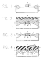
- FIGS 1--4 illustrate steps in fabrication of field-effect transistors according to this invention. For reasons of clarity, the elements of the structures depicted are not drawn to scale.
- FIGS. 1--4 An exemplary method of fabricating an integrated circuit, which includes a field-effect transistor, according to this invention will be described by reference to FIGS. 1--4.
- substrate 1 Depicted in FIG. 1 are substrate 1, and disposed thereon, are field-oxide 3 and gate structure 5.
- the field oxide regions are spaced from the gate structure, which has polysilicon layer 7, layer 9, which may be oxide or silicide and silicon nitride SiN x layer 11.
- the elements depicted are fabricated by techniques that are well known to those skilled in the art and which, therefore, need not be described in further detail. In particular, appropriate layer thicknesses will be readily selected by those skilled in the art as all considerations are well-known.
- the gate structure and the field oxide should desirably have approximately the same height, as measured from the substrate surface, although this requirement is not absolutely critical if the difference between oxide and/or nitride and polysilicon etch rates is large. That is, a later step etches back a deposited polysilicon layer to expose both the gate and the field oxide without excessive etching of either the gate top layer or the field oxide. Over-etching of either of these elements is limited if they have approximately the same height. However, this height limitation is not critical if the etch used has a relatively high selectivity between oxide or nitride, and polysilicon. Also, the silicon nitride layer can be omitted if only a single dielectric layer is desired on the gate structure. If desired, ion implantation for a lightly doped drain structure may be performed.
- sidewall spacers 13 are formed on the sides of the gate electrode structure.
- the sidewall spacers which are insulating, may be formed either by, e.g., thermal oxidation or oxide chemical vapor deposition followed by an anistropic etchback.
- An etching step desirably follows the thermal oxidation step to ensure that the spacers have a small lateral dimension.
- a polysilicon layer 15 is deposited and resist 17 spun on.
- the polysilicon is deposited to a thickness which fills in the space between the gate structure and the field oxide and covers these features.
- Any conventional polysilicon deposition technique such as, low-pressure chemical vapor deposition (LPCVD), may be used to deposit the polysilicon.
- LPCVD low-pressure chemical vapor deposition
- the polysilicon deposits in a conformal manner and need not be deposited in a thick layer.
- Source and drain regions 19 are formed.
- the field oxide is adjacent to the source/drain regions. Very shallow, e.g., 100nm to 150nm, source and drain junctions below the silicon surface are easily obtained. Alternatively, elevated source/drain regions can be formed. "Elevated” means that a significant portion of the source/drain region is above the electrical channel. If salicide source and drain regions are needed, the salicide 21 can be formed on source and drain window pads 15 using well-known techniques.
- a silicide forming transition metal is deposited after the window pad layers are formed and heated to form the silicide. It should be noted that the polysilicon and metal thicknesses can be selected so that the salicide does not extend into the source/drain regions. Source/drain junction leakage is, therefore, not a problem.
- a passivation dielectric 23 is deposited and windows are opened in the dielectric for the metallizations 25. These steps are performed using conventional and well-known techniques. The completed device is depicted in FIG. 4. Those skilled in the art will readily appreciate that an integrated circuit comprises many such interconnected devices.
Landscapes
- Insulated Gate Type Field-Effect Transistor (AREA)
- Electrodes Of Semiconductors (AREA)
Applications Claiming Priority (2)
| Application Number | Priority Date | Filing Date | Title |
|---|---|---|---|
| US42042089A | 1989-10-12 | 1989-10-12 | |
| US420420 | 1989-10-12 |
Publications (1)
| Publication Number | Publication Date |
|---|---|
| EP0422824A1 true EP0422824A1 (fr) | 1991-04-17 |
Family
ID=23666400
Family Applications (1)
| Application Number | Title | Priority Date | Filing Date |
|---|---|---|---|
| EP90310817A Withdrawn EP0422824A1 (fr) | 1989-10-12 | 1990-10-03 | Transistor à effet de champ avec des fenêtres en pavé de polysilicium |
Country Status (2)
| Country | Link |
|---|---|
| EP (1) | EP0422824A1 (fr) |
| JP (1) | JPH03138930A (fr) |
Cited By (8)
| Publication number | Priority date | Publication date | Assignee | Title |
|---|---|---|---|---|
| EP0516338A3 (fr) * | 1991-05-30 | 1994-01-19 | American Telephone & Telegraph | |
| WO1996025762A1 (fr) * | 1995-02-16 | 1996-08-22 | National Semiconductor Corporation | Transistor mos a effet de champ, a courant de fuite reduit |
| WO1997036321A1 (fr) * | 1996-03-27 | 1997-10-02 | Advanced Micro Devices, Inc. | Procede de dopage separe des zones polygrille et drain-source |
| EP0747941A3 (fr) * | 1995-06-07 | 1998-07-22 | STMicroelectronics, Inc. | Méthode pour former des régions de source/drain saillantes dans un circuit intégré |
| WO1998035380A1 (fr) * | 1997-02-10 | 1998-08-13 | Advanced Micro Devices, Inc. | Procede de fabrication de composants cmos comportant des jonctions tres peu profondes et une zone de drain limitee |
| EP0797250A3 (fr) * | 1996-03-22 | 1999-05-06 | Kabushiki Kaisha Toshiba | Méthode pour faire des contacts sur un dispositif semi-conducteur |
| US5955770A (en) * | 1994-10-31 | 1999-09-21 | Stmicroelectronics, Inc. | Method of forming raised source/drain regions in an integrated circuit |
| WO2009031085A1 (fr) * | 2007-09-05 | 2009-03-12 | Nxp B.V. | Transistor et sa méthode de fabrication |
Families Citing this family (1)
| Publication number | Priority date | Publication date | Assignee | Title |
|---|---|---|---|---|
| JP2000357666A (ja) | 1999-04-15 | 2000-12-26 | Sharp Corp | 半導体装置及びその製造方法 |
Citations (3)
| Publication number | Priority date | Publication date | Assignee | Title |
|---|---|---|---|---|
| EP0121351A1 (fr) * | 1983-03-04 | 1984-10-10 | Oki Electric Industry Company, Limited | Procédé de fabrication de dispositifs semi-conducteurs MOS |
| EP0233791A2 (fr) * | 1986-02-21 | 1987-08-26 | SGS Microelettronica SpA | Transistor à effet de champ à porte isolée et sa méthode de fabrication |
| EP0319215A2 (fr) * | 1987-12-04 | 1989-06-07 | AT&T Corp. | Procédé pour fabriquer des circuits intégrés comportant des FETs |
-
1990
- 1990-10-03 EP EP90310817A patent/EP0422824A1/fr not_active Withdrawn
- 1990-10-12 JP JP2272493A patent/JPH03138930A/ja active Pending
Patent Citations (3)
| Publication number | Priority date | Publication date | Assignee | Title |
|---|---|---|---|---|
| EP0121351A1 (fr) * | 1983-03-04 | 1984-10-10 | Oki Electric Industry Company, Limited | Procédé de fabrication de dispositifs semi-conducteurs MOS |
| EP0233791A2 (fr) * | 1986-02-21 | 1987-08-26 | SGS Microelettronica SpA | Transistor à effet de champ à porte isolée et sa méthode de fabrication |
| EP0319215A2 (fr) * | 1987-12-04 | 1989-06-07 | AT&T Corp. | Procédé pour fabriquer des circuits intégrés comportant des FETs |
Non-Patent Citations (2)
| Title |
|---|
| IEEE ELECTRON DEVICE LETTERS, vol. 9, no. 8, August 1988, pages 388-390, New York, US; C.-Y. LU et al.: "A folded extended window MOSFET for VLSI applications" * |
| RESEARCH DISCLOSURE, no. 303, July 1989, page 496, New York, US; ANONYMOUS: "Method for making devices having reduced field gradients at junction edges" * |
Cited By (14)
| Publication number | Priority date | Publication date | Assignee | Title |
|---|---|---|---|---|
| EP0516338A3 (fr) * | 1991-05-30 | 1994-01-19 | American Telephone & Telegraph | |
| US5879997A (en) * | 1991-05-30 | 1999-03-09 | Lucent Technologies Inc. | Method for forming self aligned polysilicon contact |
| US5955770A (en) * | 1994-10-31 | 1999-09-21 | Stmicroelectronics, Inc. | Method of forming raised source/drain regions in an integrated circuit |
| US5824577A (en) * | 1995-02-16 | 1998-10-20 | National Semiconductor Corporation | MOSFET with reduced leakage current |
| US5801424A (en) * | 1995-02-16 | 1998-09-01 | National Semiconductor Corporation | MOSFET with reduced leakage current |
| WO1996025762A1 (fr) * | 1995-02-16 | 1996-08-22 | National Semiconductor Corporation | Transistor mos a effet de champ, a courant de fuite reduit |
| EP0747941A3 (fr) * | 1995-06-07 | 1998-07-22 | STMicroelectronics, Inc. | Méthode pour former des régions de source/drain saillantes dans un circuit intégré |
| EP0797250A3 (fr) * | 1996-03-22 | 1999-05-06 | Kabushiki Kaisha Toshiba | Méthode pour faire des contacts sur un dispositif semi-conducteur |
| WO1997036321A1 (fr) * | 1996-03-27 | 1997-10-02 | Advanced Micro Devices, Inc. | Procede de dopage separe des zones polygrille et drain-source |
| US6319804B1 (en) | 1996-03-27 | 2001-11-20 | Advanced Micro Devices, Inc. | Process to separate the doping of polygate and source drain regions in dual gate field effect transistors |
| WO1998035380A1 (fr) * | 1997-02-10 | 1998-08-13 | Advanced Micro Devices, Inc. | Procede de fabrication de composants cmos comportant des jonctions tres peu profondes et une zone de drain limitee |
| US6015740A (en) * | 1997-02-10 | 2000-01-18 | Advanced Micro Devices, Inc. | Method of fabricating CMOS devices with ultra-shallow junctions and reduced drain area |
| WO2009031085A1 (fr) * | 2007-09-05 | 2009-03-12 | Nxp B.V. | Transistor et sa méthode de fabrication |
| US8202782B2 (en) | 2007-09-05 | 2012-06-19 | Nxp B.V. | Method of manufacturing transistor |
Also Published As
| Publication number | Publication date |
|---|---|
| JPH03138930A (ja) | 1991-06-13 |
Similar Documents
| Publication | Publication Date | Title |
|---|---|---|
| US5905293A (en) | LDD spacers in MOS devices with double spacers | |
| KR930001559B1 (ko) | 전계효과 트랜지스터 제조방법 | |
| US4319395A (en) | Method of making self-aligned device | |
| US5290720A (en) | Transistor with inverse silicide T-gate structure | |
| JP2780986B2 (ja) | 集積回路の製造方法 | |
| US6894357B2 (en) | Gate stack for high performance sub-micron CMOS devices | |
| US5663586A (en) | Fet device with double spacer | |
| JPH09283760A (ja) | 半導体素子の製造方法 | |
| JPS6249750B2 (fr) | ||
| US4822754A (en) | Fabrication of FETs with source and drain contacts aligned with the gate electrode | |
| US6225175B1 (en) | Process for defining ultra-thin geometries | |
| US5668051A (en) | Method of forming poly plug to reduce buried contact series resistance | |
| US5340761A (en) | Self-aligned contacts with gate overlapped lightly doped drain (goldd) structure | |
| EP0656645B1 (fr) | Transistor à effet de champ à jonction diffusée scellée | |
| US6117739A (en) | Semiconductor device with layered doped regions and methods of manufacture | |
| US6245625B1 (en) | Fabrication method of a self-aligned contact window | |
| US5550073A (en) | Method for manufacturing an EEPROM cell | |
| US5879997A (en) | Method for forming self aligned polysilicon contact | |
| US5288666A (en) | Process for forming self-aligned titanium silicide by heating in an oxygen rich environment | |
| US5731240A (en) | Manufacturing method for semiconductor depositing device | |
| US5610424A (en) | Metal oxide semiconductor field effect transistor | |
| US6153457A (en) | Method of fabricating self-align-contact | |
| JPH03138930A (ja) | ポリシリコン・ウィンドーパッドを有する電界効果トランジスタ | |
| EP0225426B1 (fr) | Procédé pour fabriquer un transistor du type MOS sur un substrat | |
| KR0154306B1 (ko) | 모스 트랜지스터의 제조방법 |
Legal Events
| Date | Code | Title | Description |
|---|---|---|---|
| PUAI | Public reference made under article 153(3) epc to a published international application that has entered the european phase |
Free format text: ORIGINAL CODE: 0009012 |
|
| AK | Designated contracting states |
Kind code of ref document: A1 Designated state(s): DE FR GB IT |
|
| 17P | Request for examination filed |
Effective date: 19911008 |
|
| 17Q | First examination report despatched |
Effective date: 19940113 |
|
| RAP3 | Party data changed (applicant data changed or rights of an application transferred) |
Owner name: AT&T CORP. |
|
| STAA | Information on the status of an ep patent application or granted ep patent |
Free format text: STATUS: THE APPLICATION IS DEEMED TO BE WITHDRAWN |
|
| 18D | Application deemed to be withdrawn |
Effective date: 19940726 |