EP0226794B1 - Verfahren zum Ziehen von Einkristallen mit einer Zweitiegelvorrichtung und Zweitiegelvorrichtung zur Durchführung des Verfahrens - Google Patents
Verfahren zum Ziehen von Einkristallen mit einer Zweitiegelvorrichtung und Zweitiegelvorrichtung zur Durchführung des Verfahrens Download PDFInfo
- Publication number
- EP0226794B1 EP0226794B1 EP86115638A EP86115638A EP0226794B1 EP 0226794 B1 EP0226794 B1 EP 0226794B1 EP 86115638 A EP86115638 A EP 86115638A EP 86115638 A EP86115638 A EP 86115638A EP 0226794 B1 EP0226794 B1 EP 0226794B1
- Authority
- EP
- European Patent Office
- Prior art keywords
- crucible
- holes
- molten raw
- sealing agent
- double
- Prior art date
- Legal status (The legal status is an assumption and is not a legal conclusion. Google has not performed a legal analysis and makes no representation as to the accuracy of the status listed.)
- Expired - Lifetime
Links
Images


Classifications
-
- C—CHEMISTRY; METALLURGY
- C30—CRYSTAL GROWTH
- C30B—SINGLE-CRYSTAL GROWTH; UNIDIRECTIONAL SOLIDIFICATION OF EUTECTIC MATERIAL OR UNIDIRECTIONAL DEMIXING OF EUTECTOID MATERIAL; REFINING BY ZONE-MELTING OF MATERIAL; PRODUCTION OF A HOMOGENEOUS POLYCRYSTALLINE MATERIAL WITH DEFINED STRUCTURE; SINGLE CRYSTALS OR HOMOGENEOUS POLYCRYSTALLINE MATERIAL WITH DEFINED STRUCTURE; AFTER-TREATMENT OF SINGLE CRYSTALS OR A HOMOGENEOUS POLYCRYSTALLINE MATERIAL WITH DEFINED STRUCTURE; APPARATUS THEREFOR
- C30B27/00—Single-crystal growth under a protective fluid
- C30B27/02—Single-crystal growth under a protective fluid by pulling from a melt
-
- C—CHEMISTRY; METALLURGY
- C30—CRYSTAL GROWTH
- C30B—SINGLE-CRYSTAL GROWTH; UNIDIRECTIONAL SOLIDIFICATION OF EUTECTIC MATERIAL OR UNIDIRECTIONAL DEMIXING OF EUTECTOID MATERIAL; REFINING BY ZONE-MELTING OF MATERIAL; PRODUCTION OF A HOMOGENEOUS POLYCRYSTALLINE MATERIAL WITH DEFINED STRUCTURE; SINGLE CRYSTALS OR HOMOGENEOUS POLYCRYSTALLINE MATERIAL WITH DEFINED STRUCTURE; AFTER-TREATMENT OF SINGLE CRYSTALS OR A HOMOGENEOUS POLYCRYSTALLINE MATERIAL WITH DEFINED STRUCTURE; APPARATUS THEREFOR
- C30B15/00—Single-crystal growth by pulling from a melt, e.g. Czochralski method
- C30B15/10—Crucibles or containers for supporting the melt
- C30B15/12—Double crucible methods
-
- Y—GENERAL TAGGING OF NEW TECHNOLOGICAL DEVELOPMENTS; GENERAL TAGGING OF CROSS-SECTIONAL TECHNOLOGIES SPANNING OVER SEVERAL SECTIONS OF THE IPC; TECHNICAL SUBJECTS COVERED BY FORMER USPC CROSS-REFERENCE ART COLLECTIONS [XRACs] AND DIGESTS
- Y10—TECHNICAL SUBJECTS COVERED BY FORMER USPC
- Y10T—TECHNICAL SUBJECTS COVERED BY FORMER US CLASSIFICATION
- Y10T117/00—Single-crystal, oriented-crystal, and epitaxy growth processes; non-coating apparatus therefor
- Y10T117/10—Apparatus
- Y10T117/1024—Apparatus for crystallization from liquid or supercritical state
- Y10T117/1032—Seed pulling
- Y10T117/1052—Seed pulling including a sectioned crucible [e.g., double crucible, baffle]
Definitions
- the present invention relates, in general, to a method of growing Group III-V compound semiconductor single crystals of GaAs, InP, GaP, InAs, etc., and Group II-VI compound semiconductor single crystals of ZnSe, ZnS, CdSe, etc., using a liquid encapsulation drawing-up process (LEC process), and an apparatus therefor.
- LOC process liquid encapsulation drawing-up process
- the present invention relates, in particular, to an improved method of drawing-up a single crystal using a specific double-crucible apparatus for the purpose of uniformly doping impurities in the single crystal, and an apparatus therefor.
- a method of drawing-up a single crystal using a double-crucible apparatus (hereinafter, referred to as a double-crucible method) is used for uniformly doping impurities in the single crystal. If the coefficient of impurity segregation in a molten raw material is not I, the concentration of impurity in the single crystal will vary as the single crystal is drawn up when the single crystal is grown using a single-crucible method. In order to prevent this variation, a double-crucible method is used.
- a double-crucible apparatus comprises an outer and an inner crucible.
- inner crucibles having various shapes. Double-crucible methods, such as that described above, may be classified into various categories depending on the shape of the inner crucible.
- a thin through hole is bored in the inner crucible so that molten raw material in the outer crucible is allowed to flow into the inner crucible through the thin through hole.
- the molten raw material however, barely passes through the through hole from the inner crucible into the outer one. Therefore, it is possible to keep molten raw material within the inner crucible (hereinafter, referred to as inner molten raw material) and molten raw material within the outer crucible (hereinafter, referred to as outer molten raw material).
- Inner and outer molten raw material differ in impurity concentration.
- the inner crucible is floated in outer molten raw material. Therefore, the quantity of inner molten is constant independent of the quantity of outer molten raw material.
- the impurity concentration in the inner and an outer molten raw material are set to be c/k and c, respectively, where k represents a coefficient of segregation of impurity relative to molten impurity components and c represents the desired impurity concentration in the single crystal.
- the concentration of impurity in the inner and outer molten raw materials cannot always be set to be c/k and c, respectively, and the coefficient of impurity segregation k is not always equal to a balanced one. Therefore, in practice, it may be impossible to draw up a single crystal having an absolutely constant impurity concentration.
- a specific double-crucible apparatus comprising an outer crucible and an inner crucible attached thereto.
- Such a specific double-crucible apparatus as described above is disclosed, for example in U.S. Patent No. 4,456,499 the substance of which is incorporated herein by reference, as if fully set forth.
- Fig. 5 is a cross section showing the double-crucible apparatus disclosed in that patent.
- Fig. 6 shows the impurity concentration when Sb is doped into a single crystal of Si.
- open and closed circles represent the results obtained using a single-crucible apparatus and the specific double-crucible apparatus, respectively.
- inner crucible 51 comprising a cylindrical side wall 58 and an expanded annular portion 54, is formed in outer crucible 50.
- outer crucible 50 is a space defined by outer peripheral wall 53, cylindrical side wall 58, and expanded annular portion 54.
- the surface level of liquid in outer molten material 57 is always coincident with that of inner molten raw material 56.
- inner molten raw material 56 decreases, however, it is compensated to a certain extent because outer molten material 57 flows into inner crucible 51 through thin through holes 52.
- Inner crucible 51 is not floated in outer molten material 57 and, therefore, the quantity of inner molten material 56 is not constant.
- the temperature of the molten raw materials is higher than the melting point of the same, while the temperature of single crystal 10 is lower than the melting point thereof.
- the temperature at inner surface II is, of course, equal to the melting point of single crystal 10.
- the temperature at peripheral edge Q of the inner surface II is higher than the melting point because the temperature is influenced by the temperature of outer molten raw material 4.
- the temperature at inner end point P on a top surface of outer molten raw material 4 is higher than the melting point of single crystal 10.
- a steep temperature gradient in the radial direction has to exist between the outer peripheral surface of single crystal 10 in inner crucible 2 and the inner peripheral wall of inner crucible 2.
- a vertical temperature gradient can be formed and easily controlled.
- An object of the present invention is to eliminate the disadvantages in the prior art.
- Another object of the present invention is to provide a method of growing a single crystal and an apparatus therefor, in which a single crystal containing impurities is grown through a liquid capsule process using a double-crucible apparatus.
- a method of drawing up a single crystal using a double-crucible apparatus comprises the steps of:
- a double-crucible apparatus for achieving the objects as stated above comprises:
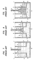
- Fig. I is a longitudinal cross section showing the portion of a double-crucible apparatus used for the double-crucible method according to the present invention.
- the double-crucible apparatus comprises outer crucible 21 having a bottom portion, and inner crucible 22, part of the bottom portion of outer crucible 21 being used by inner crucible 22 as its bottom portion.
- Outer crucible 21 and inner crucible 22 are supplied with molten raw materials 24 and 25, respectively. Since the liquid capsule process is employed, the liquid surfaces of the molten raw materials 24 and 25 are covered with liquid sealing agents 26 and 27, respectively.
- the molten raw material and sealing agent in inner crucible 22 are referred to as inner molten raw material 25 and inner sealing agent 27, respectively.
- the molten raw material and sealing agent between the outer wall of inner crucible 22 and outer crucible 21 are referred to as outer molten raw material 24 and outer sealing agent 26, respectively.
- sealing agent through holes 33 are formed in the side walls of the inner crucible 22 at its upper portions, allowing communication between outer and inner sealing agent 26 and 27, respectively.
- sealing agent through holes 33 are disposed in three stages in this embodiment, sealing agent through holes 33 may be arranged in one or two stages depending on the thickness of the sealing agent. Sealing agent through holes 33 must be arranged in at least one stage to allow communication between outer and inner sealing agent 26 and 27, respectively.
- the liquid surface of the sealing agent lowers since the liquid surface of the molten raw material lowers during the crystal growth.
- the interface between the sealing agent and the molten raw material is even in inner and outer crucible.
- the process of growing a single crystal includes a step of increasing the diameter of the single crystal so as to form a shoulder portion thereof, and a succeeding step of growing a straight body portion of the single crystal which straight body portion has a constant diameter.
- the thickness of inner sealing agent 27 varies little, and, therefore, it is not necessary for inner sealing agent 27 and outer sealing agent 26 to communicate with each other.
- sealing agent through holes 33 may be formed only in the relatively upper portions of inner crucible 22.
- sealing agent through holes 33 are provided in the upper portions of the side wall of inner crucible 22 allowing communication between outer sealing agent 26 and inner sealing agent 27 at least during the formation of the shoulder portion of the single crystal. Sealing agent through holes 33 are necessary only in the upper portions of inner crucible 22 during this step.
- the diameter of each of sealing agent through holes 33 may be selected as desired.
- the diameter of the respective must be set to such a value as to prevent free communication between outer and inner molten raw material 24 and 25, respectively. Free communication is prevented because otherwise it is impossible to maintain a difference in concentration of impurity between outer and inner molten raw material 24 and 25, respectively. To this end, it is preferable to select a diameter not larger than I mm.
- the surface tension of the molten raw material is generally larger than that of the liquid sealing agent. As the molten raw material passes through a thin hole less readily than does sealing agent, the diameter of each of molten raw material through holes 23 is often selected to be not smaller than I mm.
- Fig. I shows the state where single crystal 30 is being drawn up following seed crystal 28. Seed crystal 28 is attached to the lower end of upper shaft 29.
- Fig. 2 is a longitudinal cross section showing the step in which seeding of a single crystal is being carried out.
- inner and outer molten raw materials 25 and 24, respectively are even in surface level with each other.
- Inner and outer sealing agents 27 and 26, respectively, are also even in surface level.
- upper shaft 29 is moved down while being rotated so that seed crystal 28 is soaked into inner molten raw material 25 so as to grow single crystal 30.
- single crystal 30 following seed crystal 28 is gradually grown.
- Upper shaft 29 is then moved up while being rotated. First, the diameter of single crystal 30 is gradually increased so as to form the shoulder portion.
- the cross section of the single crystal 30 increases, so that the liquid surface level of inner sealing agent 27 increases.
- Inner sealing agent 27 flows into outer crucible 21 through sealing agent through holes 33, so that outer and inner sealing agents 26 and 27, respectively, are kept even in surface level.
- Fig. I shows the state where the formation of the shoulder portion of single crystal 30 has been completed.
- outer and inner sealing agents 26 and 27, respectively are even in surface level with each other, and outer and inner molten raw materials 24 and 25, respectively, are also even in surface level.
- the straight body portion of single crystal 30 is grown.
- the volume of the single crystal 30 in inner molten raw material 25 varies little, and, therefore, the thickness of each of inner and outer sealing agents 27 and 26, respectfully, also varies little.
- the surface level of inner sealing agent 27 drops, no difference in surface level appears either between outer and inner sealing agents 27 and 26, respectively, or between inner and outer molten raw materials 25 and 14, respectfully, even if the sealing agents drop below sealing agent through holes 33.
- Fig. 3 shows the state after the growth of the straight body portion of single crystal 30 has been completed.
- outer and inner molten raw material 24 and 25, respectfully are even in surface level and outer and inner sealing agents 26 and 27, respectfully, are also even in surface level.
- sealing agent through holes 33 in the third stage which are in contact with outer and inner sealing agents 26 and 27, respectively, the perfect evenness in surface level is maintained. It is sufficient for sealing agent through holes 33 to be provided such that the sealing agents can be in contact with sealing agent through holes 33 at least in the lowermost stage until the growth of the shoulder portion has been completed.
- a single crystal of GaAs containing Si as impurities was drawn up on the basis of the LEC process using B 2 0 3 as a liquid sealing agent.
- An outer crucible of quartz having an inner diameter of 150 mm and an inner crucible of quartz having an inner diameter of 80 mm were used.
- a polycrystal of GaAs was used as a raw material.
- the quantities of charge into the inner and outer crucibles were as follows:
- Two diametrically opposed sealing agent through holes 33 having a diameter of 3 mm were formed in inner crucible 22 at positions which are 2 mm higher than the interface between a molten raw material of GaAs and a molten sealing agent of B 2 0 3 when the charged materials GaAs and B 2 0 3 were molten.
- Two diametrically opposed molten raw material through holes 23 having a diameter of 1.5 mm were formed in inner crucible 22 at portions which are higher by about 5mm than a bottom portion thereof.
- a vessel accommodating the double-crucible apparatus therein was filled with a nitrogen gas to 106 Pa (10 atms) and a heater was energized to thereby increase the temperature of the crucibles.
- the sealing agent of B 2 0 3 was molten, and then the polycrystal of GaAs was molten.
- the molten raw material of GaAs was covered with the molten sealing agent of B 2 0 3 , the density of the latter being smaller than that of the former.
- Group V elements were prevented from separating from the molten raw material by the application of high pressure nitrogen gas.
- the thickness of the molten B 2 0 3 was about 20 mm.
- the equivalent pressure of B 2 0 3 on opposite sides of the sealing agent through holes means that the height of the surface of the molten sealing agent of B 2 0 3 on opposite sides of the sealing agent through holes are also equivalent. Since the respective molten sealing agents of B 2 0 3 in outer and inner crucibles 21 and 22, respectively, are even in surface level, the respective molten raw materials covered with the molten sealing agents of B 2 0 3 are also even in surface level. The concentration of Si in inner crucible 22 will be prevented from increasing as single crystal 30 is grown because the molten raw material containing no Si in outer crucible 21 flows into inner crucible 22.
- a single crystal of Si-doped GaAs was grown using the conventional single-crucible apparatus and the thus obtained single crystal was compared with the single crystal obtained according to the present invention.
- the Si concentration in the vicinity of the seed crystal was controlled to be 4 x 10¹⁸ atom/cm3.
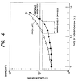
- Fig. 4 is graph showing the Si concentration at portions from the seed end (a front portion) of the crystal to the end (a back portion) opposite to the seed end of the same.
- the abscissa represents the rate of solidification, which is a value obtained by dividing the weight from the front end to a point of the crystal by the quantity of initially charged raw material.
- the rate of solidification is a parameter which closely corresponds to the distance from the seed end to the measuring point.
- the ordinate represents the Si concentration (atom/cm3) in the crystal. Closed and open circles represent the results obtained using the present invention and using the conventional single-crucible apparatus, respectively. As can be seen in Fig.
- the yield of single crystals having the Si concentration within a range of 4-8 x 10¹⁸ atom/cm 3 using the present invention was 75%.
- the yield of the single crystals was 55%.
- the yield was improved by about 36% using the present invention.
- the rate of single-crystallization obtained by using the double-crucible apparatus provided with sealing agent through holes according to the present invention was compared with that obtained using the conventional double-crucible apparatus provided with no sealing agent through holes.
- the rate of single-crystallization was 32%.
- the rate of single-crystallization was 63%. This rate of single-crystallization is the weight of a crystallized portion compared to the weight of the initially charged raw material.
Landscapes
- Chemical & Material Sciences (AREA)
- Engineering & Computer Science (AREA)
- Crystallography & Structural Chemistry (AREA)
- Materials Engineering (AREA)
- Metallurgy (AREA)
- Organic Chemistry (AREA)
- Liquid Deposition Of Substances Of Which Semiconductor Devices Are Composed (AREA)
- Crystals, And After-Treatments Of Crystals (AREA)
Claims (6)
Applications Claiming Priority (2)
| Application Number | Priority Date | Filing Date | Title |
|---|---|---|---|
| JP265489/85 | 1985-11-25 | ||
| JP60265489A JPS62128999A (ja) | 1985-11-25 | 1985-11-25 | 2重るつぼを用いた単結晶引上方法及び2重るつぼ |
Publications (2)
| Publication Number | Publication Date |
|---|---|
| EP0226794A1 EP0226794A1 (de) | 1987-07-01 |
| EP0226794B1 true EP0226794B1 (de) | 1990-10-03 |
Family
ID=17417887
Family Applications (1)
| Application Number | Title | Priority Date | Filing Date |
|---|---|---|---|
| EP86115638A Expired - Lifetime EP0226794B1 (de) | 1985-11-25 | 1986-11-11 | Verfahren zum Ziehen von Einkristallen mit einer Zweitiegelvorrichtung und Zweitiegelvorrichtung zur Durchführung des Verfahrens |
Country Status (5)
| Country | Link |
|---|---|
| US (1) | US5021118A (de) |
| EP (1) | EP0226794B1 (de) |
| JP (1) | JPS62128999A (de) |
| CA (1) | CA1317202C (de) |
| DE (1) | DE3674744D1 (de) |
Families Citing this family (5)
| Publication number | Priority date | Publication date | Assignee | Title |
|---|---|---|---|---|
| US4919901A (en) * | 1987-12-31 | 1990-04-24 | Westinghouse Electric Corp. | Barrier design for crucibles for silicon dendritic web growth |
| JP3015656B2 (ja) * | 1994-03-23 | 2000-03-06 | 株式会社東芝 | 半絶縁性GaAs単結晶の製造方法および製造装置 |
| GB9412629D0 (en) * | 1994-06-23 | 1994-08-10 | Secr Defence | Improvements in crystal growth |
| TW430699B (en) * | 1995-12-27 | 2001-04-21 | Mitsubishi Material Silicon Co | Single crystal pulling apparatus |
| JP3769800B2 (ja) * | 1996-01-12 | 2006-04-26 | 株式会社Sumco | 単結晶引上装置 |
Family Cites Families (9)
| Publication number | Priority date | Publication date | Assignee | Title |
|---|---|---|---|---|
| US2892739A (en) * | 1954-10-01 | 1959-06-30 | Honeywell Regulator Co | Crystal growing procedure |
| NL112257C (de) * | 1958-07-11 | |||
| US4352784A (en) * | 1979-05-25 | 1982-10-05 | Western Electric Company, Inc. | Double crucible Czochralski crystal growth apparatus |
| US4456499A (en) * | 1979-05-25 | 1984-06-26 | At&T Technologies, Inc. | Double crucible Czochralski crystal growth method |
| US4246064A (en) * | 1979-07-02 | 1981-01-20 | Western Electric Company, Inc. | Double crucible crystal growing process |
| DE3316547C2 (de) * | 1983-05-06 | 1985-05-30 | Philips Patentverwaltung Gmbh, 2000 Hamburg | Kalter Tiegel für das Erschmelzen nichtmetallischer anorganischer Verbindungen |
| JPS60176997A (ja) * | 1984-02-23 | 1985-09-11 | Sumitomo Electric Ind Ltd | 低転位密度の3−5化合物半導体単結晶 |
| JPS60251191A (ja) * | 1984-05-25 | 1985-12-11 | Res Dev Corp Of Japan | 高解離圧化合物単結晶成長方法 |
| JPS6426591A (en) * | 1987-07-20 | 1989-01-27 | Yasumitsu Tamura | Anthracyclines or anthracyclinones not containing hydroxyl group at 11-position |
-
1985
- 1985-11-25 JP JP60265489A patent/JPS62128999A/ja active Pending
-
1986
- 1986-11-11 EP EP86115638A patent/EP0226794B1/de not_active Expired - Lifetime
- 1986-11-11 DE DE8686115638T patent/DE3674744D1/de not_active Expired - Lifetime
- 1986-11-19 CA CA000523332A patent/CA1317202C/en not_active Expired - Fee Related
- 1986-11-24 US US06/933,924 patent/US5021118A/en not_active Expired - Fee Related
Also Published As
| Publication number | Publication date |
|---|---|
| US5021118A (en) | 1991-06-04 |
| EP0226794A1 (de) | 1987-07-01 |
| CA1317202C (en) | 1993-05-04 |
| DE3674744D1 (de) | 1990-11-08 |
| JPS62128999A (ja) | 1987-06-11 |
Similar Documents
| Publication | Publication Date | Title |
|---|---|---|
| US4894206A (en) | Crystal pulling apparatus | |
| US3033660A (en) | Method and apparatus for drawing crystals from a melt | |
| US4980015A (en) | Method for pulling single crystals | |
| US4911780A (en) | LEC method for growing a single crystal of compound semiconductors | |
| US4352784A (en) | Double crucible Czochralski crystal growth apparatus | |
| US4944834A (en) | Process of pulling a crystal | |
| US4863554A (en) | Process for pulling a single crystal | |
| KR920009563B1 (ko) | 반도체 결정의 인상 방법 | |
| EP0226794B1 (de) | Verfahren zum Ziehen von Einkristallen mit einer Zweitiegelvorrichtung und Zweitiegelvorrichtung zur Durchführung des Verfahrens | |
| US4664742A (en) | Method for growing single crystals of dissociative compounds | |
| US5073229A (en) | Semiconductor crystal pulling method | |
| US4944925A (en) | Apparatus for producing single crystals | |
| US5471943A (en) | Process and device for pulling crystals according to the Czochralski method | |
| US4456499A (en) | Double crucible Czochralski crystal growth method | |
| EP0141649A1 (de) | Vorrichtung zur Züchtung eines Einkristalls | |
| EP0355833B1 (de) | Verfahren zur Herstellung eines Einkristalls aus einer Halbleiter-Verbindung | |
| JPH06128096A (ja) | 化合物半導体多結晶の製造方法 | |
| WO1986006109A1 (en) | Method and apparatus for growing single crystal bodies | |
| JPS61266389A (ja) | 結晶内不純物均一化用二重るつぼ | |
| KR920007340B1 (ko) | Ⅲ-ⅴ화합물 반도체 단결정의 제조방법 | |
| JPS61158896A (ja) | 化合物半導体単結晶の製造方法と装置 | |
| JPH0699228B2 (ja) | 単結晶の引上方法 | |
| JP3013125B2 (ja) | 引き上げ成長方法及び装置 | |
| JPH08104591A (ja) | 単結晶成長装置 | |
| JPH03261694A (ja) | 単結晶の引上方法および引上装置 |
Legal Events
| Date | Code | Title | Description |
|---|---|---|---|
| PUAI | Public reference made under article 153(3) epc to a published international application that has entered the european phase |
Free format text: ORIGINAL CODE: 0009012 |
|
| AK | Designated contracting states |
Kind code of ref document: A1 Designated state(s): DE FR GB |
|
| 17P | Request for examination filed |
Effective date: 19870722 |
|
| 17Q | First examination report despatched |
Effective date: 19890223 |
|
| GRAA | (expected) grant |
Free format text: ORIGINAL CODE: 0009210 |
|
| AK | Designated contracting states |
Kind code of ref document: B1 Designated state(s): DE FR GB |
|
| ET | Fr: translation filed | ||
| REF | Corresponds to: |
Ref document number: 3674744 Country of ref document: DE Date of ref document: 19901108 |
|
| PLBE | No opposition filed within time limit |
Free format text: ORIGINAL CODE: 0009261 |
|
| STAA | Information on the status of an ep patent application or granted ep patent |
Free format text: STATUS: NO OPPOSITION FILED WITHIN TIME LIMIT |
|
| 26N | No opposition filed | ||
| PGFP | Annual fee paid to national office [announced via postgrant information from national office to epo] |
Ref country code: FR Payment date: 19991109 Year of fee payment: 14 |
|
| PGFP | Annual fee paid to national office [announced via postgrant information from national office to epo] |
Ref country code: GB Payment date: 19991110 Year of fee payment: 14 |
|
| PGFP | Annual fee paid to national office [announced via postgrant information from national office to epo] |
Ref country code: DE Payment date: 19991115 Year of fee payment: 14 |
|
| PG25 | Lapsed in a contracting state [announced via postgrant information from national office to epo] |
Ref country code: GB Free format text: LAPSE BECAUSE OF NON-PAYMENT OF DUE FEES Effective date: 20001111 |
|
| GBPC | Gb: european patent ceased through non-payment of renewal fee |
Effective date: 20001111 |
|
| PG25 | Lapsed in a contracting state [announced via postgrant information from national office to epo] |
Ref country code: FR Free format text: LAPSE BECAUSE OF NON-PAYMENT OF DUE FEES Effective date: 20010731 |
|
| PG25 | Lapsed in a contracting state [announced via postgrant information from national office to epo] |
Ref country code: DE Free format text: LAPSE BECAUSE OF NON-PAYMENT OF DUE FEES Effective date: 20010801 |
|
| REG | Reference to a national code |
Ref country code: FR Ref legal event code: ST |